UNIVERSITÀ DEGLI STUDI DI CATANIA
D
IPARTIMENTO DII
NGEGNERIAE
LETTRICAE
LETTRONICA EI
NFORMATICAD
OTTORATO DIR
ICERCAI
NTERNAZIONALEE
NERGETICAXXVII
CICLOALESSIA AVOLA
Analysis and Reduction of Conducted EMI
in Power Electronic Modules
Ph. D. Thesis
Coordinator: Chiar.mo Prof. Ing. L. Marletta
Tutor: Chiar.mo Prof. Ing. G. Aiello
i
Contents
Introduction ... 1
Chapter 1 Power electronic systems ... 3
1.1 Power electronic ... 3
1.2 Applications of power electronics system ... 4
1.3 Power converters ... 6
1.4 Power electronic devices ... 7
1.4.1 The power diode ... 10
1.4.2 Control switch devices ... 14
1.4.1.1 BJT ... 14
1.4.1.2 Mosfet ... 17
1.4.1.3 GTO ... 20
1.4.1.4 MCT ... 22
1.4.1.5 IGBT ... 24
1.4.1.6 Comparison of controllable switches ... 27
Chapter 2 Electromagnetic interference ... 29
2.1 Introduction to electromagnetic compatibility ... 29
2.2 Conducted EMI ... 33
2.3 EMC regulations ... 36
ii
3.1 Structure and materials of power modules ... 40
Chapter 4 Numerical methods in electromagnetism and simulation tools ... 49
4.1 Generality on numerical methods ... 49
4.2 Finite Element Method ... 51
4.2.1 Generality ... 51
4.3 FEM and electromagnetism ... 53
4.3.1 Finite Elements and shape function ... 53
4.3.2 The equations of the electromagnetic field ... 57
4.3.3 The equations of electric quasi - stationary field ... 59
4.3.3.1 Electric quasi-stationary analysis ... 60
4.3.3.2 Electrostatic analysis ... 61
4.3.4 The equations of magnetic quasi-stationary field ... 61
4.4 FEM algebraic system ... 65
4.5 The FEM for problems in unbounded domains ... 66
4.6 The Partial Element Equivalent Circuit Method ... 67
4.6.1 Generality ... 67
4.6.2 Partial Element Equivalent circuit for conductors ... 71
4.7 Method of Moments ... 78
4.8 Q3D Extractor software ... 80
4.9 PSpice software ... 82
Chapter 5 Analysis and reduction of conducted EMI in a power electronic module ... 84
iii
5.1 Description ... 84
5.2 Analysis ... 89
5.3 Simulation of the power electronic module ... 93
5.3.1 Time domain analysis ... 96
5.3.2 Frequency domain analysis ... 104
Conclusions ... 109
1
Introduction
The phenomena causing the production and spreading of unwanted electromagnetic emissions arising from electrical or electronic devices, apparatuses and systems have been widely investigated over the last decades and reported in the relevant scientific literature. As a consequence of this, nowadays, the electromagnetic compatibility techniques, which limit the undesirable effects of these emissions, are very popular and of ever-increasing importance both in environmental and industrial contexts.
The present thesis focuses on conducted electromagnetic emissions generated by power electronic modules making use of active devices operating with high switching frequency, which today are commonly utilized in a lot of sectors: aerospace, commercial, industrial, residential, telecommunication, transportation, utility systems. The onerous operating conditions of such modules, caused by high values of voltages and electric currents and very short switching times of active devices, make essential, in order to reach an efficient and economic use of materials and components, as well as a reliable and durable use of devices themselves, to carry out an accurate preliminary analysis of the mechanisms resulting in unwanted electromagnetic couplings between the various module components. Indeed, due to the unavoidable presence of parasitic inductances and capacitances and of extremely steep waveforms, electrical signals frequently originate inside the modules with high peak values and exasperated temporal dynamics, which strongly restrict the field of application of the modules themselves. For the sake of concreteness, the analysis of above described phenomena has been worked out on a power electronic module prototype made kindly available by STMicroelectronics, one of the world-leading companies in such field. After a first phase during of which have been
2 individuated and computed the values of the most critical parasitic elements, by means of a theoretical investigation supported by suitable software tools, attention has been paid to how to reduce such values and improve the overall performance of the module. In this connection, some useful techniques to reduce significantly the undesirable emissions have been individuate and successfully applied to the prototype, so obtaining an optimized module from the electromagnetic emission point of view.
The present thesis is structured as follows. Chapter 1 provides an introduction to main kinds of power modules used in many areas of electrical and electronic engineering and shows also the most critical features of their operations. Chapter 2 highlights the basic aspects of electromagnetic emissions focusing on the conducted ones. Chapter 3 illustrates the structure and materials of power electronic modules. In the Chapter 4 the fundamental equations of electromagnetism are briefly reviewed and the most powerful numerical methods used to solve them are described; moreover, the simulation tools Q3D Extractor and PSpice utilized in the thesis are synthetically illustrated. Chapter 5 describes in detail the analyses carried out of STMicroelectronics prototype and the original techniques and results which have been obtained. Finally, some concluding remarks complete the work.
3
Chapter 1
Power electronic systems
1.1 Power electronic
Power Electronic is one of the most important branch of electronics and electrical engineering and its aim is to process and control the flow of electrical energy by supplying voltages and currents suitable for user loads [1].
Fig. 1.1 shows the basic structure of Power Electronic System [2]. In input is given a form of electric energy and the task of the system is to convert it in another form. For example, if the load is a DC motor, then it needs a DC voltage and current, and the power controller converts the AC input into a DC values which are suitable for the motor. Inside a black box could be a controller or converter, which make use of actives devices such as thyristor, GTO, MOSFET, BJT or IGBT.
4
1.2 Applications of power electronics system
There are many applications coming up every day in power electronics. Some of them are mentioned below [3], [5]:
1. Switch mode power supplies and UPS (Uninterruptible Power Supply): advances in microelectronic technology have led to the development of computers, apparatus, communications and consumer electronics devices that require regulated dc power supplies and often continuous supply;
2. Energy Conservation: the rising costs of energy and interest in environmental protection led to give priority to energy saving. One of the applications of power electronics regards the fluorescent lamps that operate at high frequency (20 kHz) to obtain a high yield. The power electronics is also found in the motors driving pumps and compressors;
3. Transportation: the electric-drive vehicles require battery chargers that use the power electronics;
4. Electro technical applications: equipment for welding, electroplating or induction heating;
5. Utility related applications: one of these applications is in transmission of electric power with high-voltage dc lines (HVDC: High Voltage Direct Current).
Table 1.1 shows some important applications of power electronics systems. The power ratings range from a few W in the case of lamps to several 100 MW in HVDC transmission systems.
5
Table 1.1 Some application of power electronic
N. Area Application
1 Aerospace Space shuttle power supplies, Satellite power supplies,
Aircraft power system;
2 Commercial
Heating, air-conditioning power supplies, computer, office equipment, elevators, light dimmer, central refrigeration;
3 Industrial
Arc and industrial furnaces, blowers and fans, pumps and compressors, industrial lasers, transformer tap charges, rolling mills, factory automation;
4 Residential
Air conditioning, cooking, lighting, refrigerators, electric-door openers, dryers, fans, personal
computers, vacuum cleaners, washing machine, food mixers;
5 Telecommunication Battery charges, power supplies;
6 Transportation
Battery charges, traction control of electric vehicles, electric locomotives, street cars, trolley buses, subways, automotive electronics;
7 Utility Systems
High voltage DC transmission, excitation systems, VAR compensation, static circuit breakers, fans and boiler feed pumps, Grid interface for alternative energy resources (solar, wind, fuel cells, etc.) and energy storage.
6
1.3 Power converters
One of the most important typology power system are the electronic converters, by means of which it is possible to control and transform the electric power. The power electronic converters are generally classified into five categories depending on the input, output and job they perform:
1. AC to DC Converters; 2. DC to AC Converters; 3. DC to DC Converters; 4. AC to AC Converters; 5. AC Regulators.
Power converters have many advantages, such as: high efficiency of conversion due to low losses in power semiconductor device, long life, compact size and light weight, fast dynamic response, lower installation costs and high reliability of power electronic components and converter systems.
Power Converters introduce harmonics into supply and load systems, adversely affecting the performance of the load and supply. These harmonics distort the voltage waveform and cause interference with communication lines. To devoid these, it is necessary to insert a filter at the input of a converter [2],[4]. Although these disadvantages power electronic converters are used in large number of applications.
7
1.4 Power electronic devices
One of the main contributions that led to the growth of the power electronics field has been the unprecedented advancement in semiconductor technology, especially with respect to switching speed and power handling capabilities. The area of power electronics started by the introduction of the silicon controlled rectifier (SCR) in 1958. Since then, the field has grown in parallel with the growth of the power semiconductor device technology. In fact, the history of power electronics is very much connected to the development of switching devices and it emerged as a separate discipline when high-power and MOSFET devices were introduced in the 1960s and 1970s. The introduction of new devices has been ever accompanied by dramatic improvement in power rating and switching performance. Because of their functional importance, drive complexity, fragility, and cost, the power electronic design must be equipped with a thorough understanding of the device operation, limitation, drawbacks, and related reliability and efficiency issues. In the 1980s, the development of power semiconductor devices took an important turn when a new process technology was developed that allowed integration of MOS and bipolar junction transistor (BJT) technologies on the same chip. Thus far, two devices using this new technology have been introduced: insulated bipolar transistor (IGBT) and MOS controlled thyristor (MCT). Even though, most of today’s available semiconductor power devices are made of silicon or germanium materials, other materials such as gallium arsenide, diamond and silicon carbide are currently being tested. In fact, there are several technologies emerging that are destined to replace the silicon power MOSFET as the power semiconductor transistor of choice. Currently, the most promising technologies are GaN (gallium nitride) and SiC (silicon carbide). Both
8 technologies are wide band gap materials that offer the advantages of higher power densities, higher voltages, lower leakage current and the ability to operate at higher
temperatures [27]. Power semiconductor devices represent the ‘‘heart’’ of modern power
electronics, with two major desirable characteristics of power semiconductor devices guiding their development:
1. switching speed (turn-on and turn-off times);
2. power handling capabilities (voltage blocking and current carrying capabilities).
Improvements in both semiconductor processing technology and manufacturing and packaging techniques have allowed power semiconductor development for high-voltage and high current ratings and fast turn-on and turn-off characteristics. The availability of different devices with different switching speeds, power handling capabilities, size and cost, makes it possible to cover many power electronics applications.
Power semiconductor devices can be classified into various categories according to their degree of controllability (Turn ON and Turn OFF Capability), type of gate signal required, Current Conduction Capability and Voltage withstanding ability [2], [4], [5].
1. Based on Turn ON and Turn OFF capability:
· Group I: uncontrollable power semiconductor devices such as diodes. These are called uncontrolled devices because their ON and OFF states are not dependent on the control signals but on supply and load circuit conditions;
9 · Group II: partially controllable power semiconductor devices. These include devices that are trigged into conduction by control signals but are turned off by the load circuit or by the supply. Such devices include thyristors such as line commutated SCR, force commutated SCR, light active SCR, TRIAC, DIAC;
· Group III: Fully controllable power semiconductor devices. They can be turned on and off by control signals. This group includes: BJTs, MOSFETs, IGBTs; GTOs.
2. Based on Gate signal:
· Group I: Pulse gate requirement. To Turn on these devices, pulse voltage is applied as a control signal. Once the device is turned on, the gate pulse is not required and thus removed. This group includes: SCR, GTO, SITH, MCT;
· Group II: Continuous gate requirement. For these devices, continuous gate signal is required to maintain them in ON state. This group includes: BJT, MOSFET, IGBT.
3. Based on Current Conduction Capability:
· Group I: Unidirectional Current Devices. This group includes: SCR, GTO, BJT, MOSFET, IGBT;
· Group II: Bidirectional Current Devices. This group includes: TRIAC, RCT (Reverse Conducting Thyristor).
4. Based on Voltage withstanding ability:
· Group I: Unipolar voltage withstanding devices. This group includes: BJT, MOSFET, IGBT;
10 · Group II: Bipolar voltage withstanding devices. This group includes: SCR, GTO.
1.4.1 The power diode
Power diodes play a significant role in the operation of power electronic circuits. A power diode behaves as a switch with uncontrolled turn on and turn off characteristics. There are mainly used as uncontrolled rectifiers to convert single-phase or three-phase AC voltage to DC. Diode can be constructed with germanium and silicon, but a silicon material is better because silicon diodes can work at higher current and junction temperatures than germanium diodes [6]. Fig. 1.2 (a) and (b) shows the structure of a diode and the circuit symbol of power diode respectively.
(a) (b)
Fig. 1.2 (a) p-n junction, (b) circuit symbol of power diode
The terminal voltage and current are represented as Vd and Id respectively. It has two terminals: an anode (A) and a cathode (K).
When anode (A) is positive with respect to cathode (K), the pn-junction becomes forward- biased and the diode starts to conductive. The diode does not conduct when the voltage between anode to cathode is negative, in this case, the diode is reverse biased.
11 Fig. 1.2 (b) shows the conventional direction of current flow (from anode to cathode) when diode conducts.
The structure of the power diode is little different from the small signal diodes [2].
Fig. 1.3 Structure of power diode
As shown in Fig. 1.3, there is heavily doped n+ substrate with doping level of 1019/cm3. This substrate forms a cathode of the power diode. On n+ substrate, lightly doped n- epitaxial layer is grown, this layer is also known as drift region. The PN junction is formed by diffusing a heavily doped p+ region, which is the anode of the diode. The thickness of n-drift region determines the breakdown voltage of the diode. Its function is to absorb the depletion layer of the reverse biased p+n- junction. As it is lightly doped, it will add significant ohmic resistance to the diode when it is forward biased. For higher breakdown voltages, the drift region is wide. The n-drift region is absent in low power signal diodes.
When the power diode is forward biased (anode is made positive with respect to cathode), the holes will be injected from the p+ region into the drift region. Some of the holes combine with the electrons in the drift region. Since injected holes are many, they
12 attract electrons from the n+ layer. Thus holes and electrons are injected in the drift region simultaneously and the resistance of the drift region reduces significantly. Thus diode current goes on increasing, but drift region resistance remains constant. So on-state losses in the diode are reduced. This phenomenon is called Conductivity Modulation of drift region.
Fig. 1.4 Diode: a) i-v characteristics, b) idealized characteristics
The I-V characteristics of power diode are shown in Fig. 1.4 (a). When the diode is in the forward biased condition (1st quadrant of the voltage versus current plot), it begins to conduct with only a small forward voltage across it (≈ 1 V). In reverse biased, (3th quadrant) only a negligibly small leakage current flows through the device until the reverse break-down voltage is reached [5]. Fig. 1.4 (b) shows the I-V characteristics idealized. At turn-ON, the diode can be considered an ideal switch because it turns on rapidly compared to the transients in the power circuit. At turn-OFF the diode current reverses for a reverse-recovery time trr, as indicated in Fig. 1.4.
13
Fig. 1.5 Diode turn-off
Depending on the application requirements, there are various types of diodes:
· Schottky diode: this class of diode uses metal-to-semiconductor junction to
produce the rectifying effect [7]. They are characterized by very fast reverse recovery time and low forward voltage drop (≈ 0,3 V). Schottky diodes are highly suitable for use in high-frequency applications [7];
· Fast-recovery diodes: for these diode is need a small reverse-recovery time. This group of diodes is used in combination with controllable switches [5].
· Line-frequency diodes: this group of diodes has an high value of trr. These diodes are available with blocking voltage ratings of several kV and current ratings of several kA. These diodes can be connected in series and parallel to satisfy any voltage and current requirement.
14
1.4.2 Control switch devices
As it is mentioned before the control switch can be turned on and off by control signals applied to the control terminal of the device. This kind of devices includes: BJTs, MOSFETs, GTOs and IGBTs.
1.4.2.1 BJT
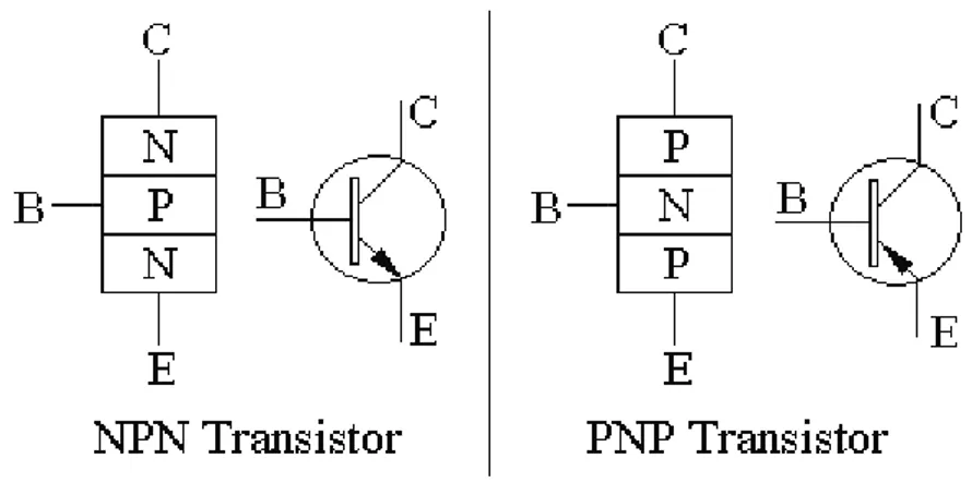
Bipolar Junction Power Transistors are applied to a variety of power electronic functions such as switching mode power supplies, dc motor inverters and PWM inverters but is mostly used in amplifiers [8]. The power BJT (Bipolar Junction Transistor) is a three terminal device and it comes in two different types: the npn BJT and the pnp BJT. The three terminals are emitter (E), collector (C) and base (B). The structure and the circuit symbol of the BJT are shown in Fig. 1.6.
Fig. 1.6 Structures and symbol of npn BJT and pnp BJT.
The BJT is fabricated with three separately doped regions and has two junctions (boundaries between the n and the p regions) which are similar to the junctions we saw in
15 the diodes and thus they may be forward biased or reverse biased. Since each junction has two possible states of operation (forward or reverse bias) the BJT with its two junctions has four possible states of operation.
The structure, as shown on Fig. 1.6, is not symmetric; the n and p regions are different both geometrically and in terms of the doping concentration of the regions. For example, the doping concentrations in the collector, base and emitter may be 1015, 1017, and 1019 respectively. Therefore the behavior of the device is not electrically symmetric and the two ends cannot be interchanged.
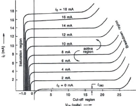
Fig. 1.7 shows the qualitative characteristic curves of a BJT. The collector current IC is plotted with respect to collector base voltage (VCB) for different values of base current (IE). Each curve starts at IC=0 and rises rapidly for a small positive increase in VCB.
16 The plot indicates the four regions of operation: the saturation, the cutoff, the active and the breakdown.
1. Cutt-off region: is the area where base current is almost zero. Hence no current flows and transistors is OFF;
2. Saturation region: The portion of the characteristics where VCB is negative; here a BJT is said to be satured when both the C-B and E-B junctions are forward-biased.
3. Active region: is defined where flat, horizontal portions of voltage-current curves show ‘‘constant’’ IC current, because the collector current does not change significantly with VCB for a given IE. Those portions are used only for small signal transistors operating as linear amplifiers [9];
4. Breakdown region: is defined when VCB voltage exceeds certain limits, becoming
practically vertical. It is good to avoid getting into this region because the transistor may be damaged or over-current or over-dissipation.
Power BJTs have good on-state characteristics but long switching times especially at turn-off. They are current controlled devices with small current gain because of high level injection effects and wide base width required to prevent reach-through breakdown for high blocking voltage capability. Therefore, they require complex base-drive circuits to provide the base current during on-state, which increases the power loss in the control electrode [9].
17
1.4.2.2 MOSFET
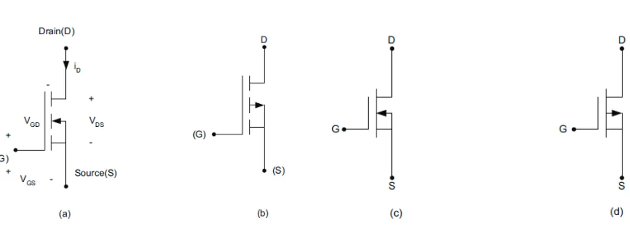
The power MOSFET (Metal Oxide Semiconductor Field Effect Transistor) belongs to the unipolar device family because it uses only majority carriers in conduction [9]. The device symbol for a p- and n-channel enhancement and depletion types are shown in Fig. 1.8.
Fig. 1.8 Device symbols: (a) channel enhancement-mode; (b) p-channel enhancement-mode; (c) n-channel depletion-mode; and (d) p-n-channel depletion-mode.
Most MOSFET devices used in power electronics applications are of the n-channel, enhancement type, like that shown in Fig. 1.8 a.
The MOSFET has three terminals: G (gate), D (drain) and S (source). It is a voltage-controlled device [5], in fact to carry drain current, a channel between the drain and the source must be created. This occurs when the gate-to-source voltage (VGS) exceeds the device threshold voltage VTh [9]. When the device is turns on and the current flows from drain to source.
Power MOSFETs use vertical channel structure in order to increase the device power rating [10]. Figure 1.9 shows a structure of n-channel enchancemode MOSFET.
18
Fig. 1.9: Structure of n-channel enchance mode MOSFET.
Most power MOSFETs feature a vertical structure with Source and Drain on opposite sides of the wafer in order to support higher current and voltage. The p-n junction between the p-base and the n-drift region provide the forward voltage blocking capabilities. The source metal contact is connected directly to the p-base region through a break in the n-source region in order to allow for a fixed potential to the p-base region during normal device operation. When the gate and source terminal are set to the same potential (VGS꞊0), no channel is established in the p-base region that is, the channel region remains unmodulated. The lower doping in the n-drift region is needed in order to achieve higher drain voltage blocking capabilities.
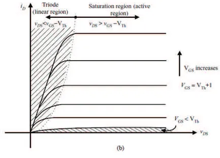
Fig. 1.10 shows the V-I characteristics of n-channel power MOSFET. The drain current iD is plotted with respect to drain source voltage VDS. These characteristics are plotted for various values of gate source voltage (VGS).
19
Fig. 1.10 n-channel enhancement-mode MOSFETcharacteristic curve.
In Fig. 1.10 we can see three regions: Triode (linear region), saturation region (active region) and cut-off region. For VGS > VTh, the device can be either in the triode region or in the saturation region, depending on the value of VDS. For given VGS, with small VDS (VDS < VGS - VTh), the device operates in the triode region and for larger VDS (VDS > VGS - VTh), the device enters in the saturation region. For VGS < VTh, the device turns off, with drain current almost equal to zero. Under both regions of operation, the gate current is almost zero. This is why the MOSFET is known as a voltage-driven device and, therefore, requires simple gate control circuit. In the power electronic applications MOSFET is never operated in the active region because it acts as amplifier. For switching applications, MOSFET is operated only in triode and cut-off regions.
Because the MOSFET is a majority carrier transport device, it is inherently capable of high frequency operation [5],[9], [12]. However, the MOSFET has two limitations: 1. high input gate capacitances;
20 2. transient/delay due to carrier transport through the drift region.
1.4.2.3 GTO
The GTO (Gate Turn - Off Thyristor) is an alternative to SCR (Silicon Controlled Rectifier) better known as a Thyristor. A SCR device has been used in large power application because of high current density and low forward voltage drop. This device has two inconvenient: they are not able to turn off through a gate and the low switching speed. For this reason the GTOs was proposed as an alternative to SCR [9].
The GTO belongs to a thyristor family with a four-layer structure. Thyristors (SCR – Silicon Controlled Rectifier) are multijunction semiconductor devices with latching behavior. Thyristors in general can be switched with short pulses, and then maintain their state until current is removed. They act only as switches. The characteristics are especially well-suited to controllable rectifiers, although thyristors have been applied to all power conversion applications [9]. A GTO device has three-terminal, anode (A),
cathode (C) and gate (G) and four layers, pnpn, as like conventional thyristors. GTOs have many applications, including motor drives, induction heating, distribution lines, pulsed power, and flexible ac transmission systems [9], [13]. The GTO behaves like thyristor except for turn-off. The GTO is a power switching device that can be turned on by a short pulse of gate current (short-duration gate current pulse) and unlike the thyristor, GTOs turned off by a reverse gate pulse (negative gate-cathode voltage). Once in the on state, the device may stay on without any further gate current. Hence there is no need for an external communication circuit to turn it off. Because turn-off is provided by bypassing carriers directly to the gate circuit, its turn-off time is short, thus giving it more
21 capability for high-frequency operation than thyristors. The GTO symbol and static
characteristics (similar to that of SCR) are shown in Fig. 1.11.
Fig. 1.11 GTO circuit symbol (a) I-V characteristics.
The structure is shown in Fig. 1.12
22 The basic structure of a GTO, a four-layer p-n-p-n semiconductor device, is very similar in construction to a thyristor. It has several design features that allow it to be turned on and off by reversing the polarity of the gate signal. The most important differences are that the GTO has long narrow emitter fingers surrounded by gate electrodes and no cathode shorts.
The advantages of this device are: higher voltage blocking capability, gate has full control over the operation of GTO, low on state loss, high ratio of peak surge current to average current and high on state gain. The GTOs have some limitations too: they require large negative gate currents for turn off, for this reason they are suitable for low power applications, very small reverse voltage blocking capability and a very small switching frequencies [2].
1.4.2.4 MCT
The power MCT (MOS Controlled Thyristor) is a new type of device that combines the capabilities of thyristor voltage and current with MOS gated turn on and off [14].In fact uses a pair of MOSFETs to turn on and turn off current. In this way MCTs overcomes some limitations of the existing power device, such as high input low current density and high forward drop of power MOSFETs, both of which do not make it suitable in low voltage and low power applications [9]. A MCT has a thyristor type structure with three junctions and pnpn layers between the anode and cathode.
23
Fig. 1.13 MCT circuit symbol.
Fig. 1.14 MCT I-V characteristic.
From the I-V characteristic, shown in Fig. 1.14, it is possible to see that the MCT has many of the property of a GTO, including a low voltage drop in the on state at relatively high currents and a latching characteristic. This device has two significant advantages over the GTO:
1. Not require a large negative gate current for turn off;
24
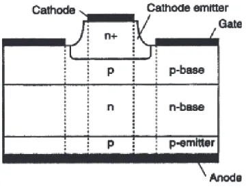
1.4.2.5 IGBT
The IGBT (Insulated Gate Bipolar Transistor) was introduced in the early 1980s becoming a successful device because of its superior characteristics. It is a three-terminal power semiconductor device that combines the simple gate-drive characteristics of the MOSFETs with the high-current and low-saturation-voltage capability of BJT [15]. The three terminals are: gate (G), collector (C) and emitter (E). Fig. 1.15 shows the symbol of IGBT.
Fig. 1.15 IGBT circuit symbol.
The current flows from collector to emitter whenever a voltage between gate and emitter is applied. In this case the IGBT is in ON state. The IGBT is in OFF state when gate emitter voltage is removed. Thus gate has full control over the conduction of IGBT. The Fig. 1.16 shows the vertical cross-section of this devise. The structure of IGBT is similar
to that of MOSFET except that n+ layer at the drain in a power MOSFET is replaced by
25
Fig. 1.16 Structure of IGBT.
IGBT is a voltage controlled device. It has high input impedance like a MOSFET and low on-state conduction losses like a BJT. When collector and gate voltage is positive with respect to emitter the device is in forward blocking mode. When gate to emitter voltage becomes greater than the threshold voltage of IGBT, a n-channel is formed in the P-region. Now device is in forward conducting state. In this state p+ substrate injects holes into the epitaxial n− layer. Increase in collector to emitter voltage will result in increase of injected hole concentration and finally a forward current is established.
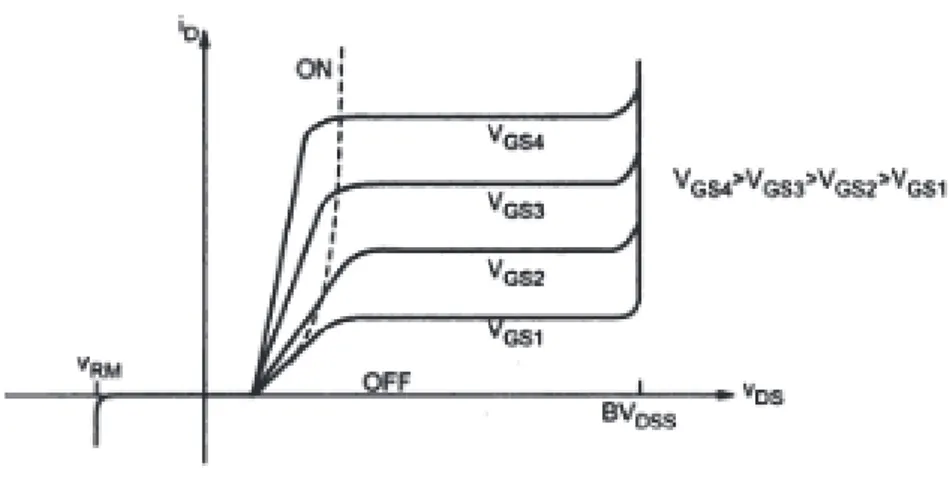
Fig. 1.17 shows the V-I characteristics of n-channel IGBT. The collector is also called Drain and emitter Source. The drain current iD is plotted with respect to drain source voltage VDS. These characteristics are plotted for various values of gate source voltage (VGS). When the gate to source voltage is greater than the threshold voltage VGS(th) the device is in ON state; when VGS is less than VGS(th) the IGBT is turns off. The BVDSS is the breakdown drain to source voltage when gate is open circuited.
26
Fig. 1.17 V-I characteristics of IGBT.
IGBTs are faster than BJT’s, but still not quite as fast as MOSFET’s. the IGBT’s offer for superior drive and output characteristics when compared to BJT’s. IGBT’s are suitable for high voltage, high current and frequencies up to 20kHz. IGBT’s are available up to 1400V, 600A and 1200V, 1000A. IGBTs are used in medium power applications such as ac and dc motor drives, medium power supplies, solid state relays and contractors, general purpose inverters, UPS, welder equipments, servo controls, robotics, cutting tools, induction heating.
27
1.4.2.6 Comparison of controllable switches
The efficiency, capacity, and ease of control of power converters depend mainly on the power devices employed. The progress in semiconductor technology will undoubtedly lead to higher power ratings, faster switching speeds and lower costs. A summary of power device capabilities is shown in Table 1.2 [5].
Table 1.2 Relative properties of controllable switches
Device Power Capability Switching Speed
BJT Medium Medium
MOSFET Low Fast
GTO High Slow
IGBT Medium Medium
MCT Medium Medium
The Fig. 1.18 represents a summary of power device capabilities. All device, except the MCT, have a relatively mature technology. MCTs technology is in a state of rapid expansion, and significant improvements in the device capabilities are possible, as indicated by the expansion arrow in the Fig.1.18.
28
29
Chapter 2
Electromagnetic interference
2.1 Introduction to electromagnetic compatibility
A system is Electromagnetic Compatible (EMC) with its environment when it is able to function compatibly with other electronic systems and not produce or be susceptible to interference. Precisely a system is electromagnetically compatible with its environment if it satisfies the following three criteria:
1. It does not cause interference with other systems;
2. It is not susceptible to emissions from other systems;
3. It does not cause interference with itself.
Constructors of devices must respect not only the desired functional performance, but also legal requirements in force in all countries of the world before to sale the product. In essence, Electromagnetic Compatibility (EMC) deals with interferences and the prevention of it through the design of electronic systems. The emissions should not be considered all undesirable phenomena, because nowadays there are many devices are specifically designed to emit EM radiation (for example: radio transmitters / television, phones mobile). The emissions due to the geometry and structure of the device must be limited as much as possible because they represent the leading cause of malfunction.
30 The EMC problem can be divided into two major sub-problems: Emission (EMI) and susceptibility (EMS).
1. Emission pertain to the interference-causing potential of a product. The purpose of controlling emissions is to limit the electromagnetic energy emitted and thereby to control the electromagnetic environment in which other products must operate;
2. Susceptibility is the capability of a device or circuit to respond to unwanted electromagnetic energy (i.e. noise). The opposite of it is immunity that gives a measure of the ability of an apparatus to receive unwanted signals (and therefore be disturbed) [17].
Eelectromagnetic Compatibility is related to the generation, transmission and reception of electromagnetic energy [16]. These three aspects form the basic structure of each project to electromagnetic compatibility which is illustrated in Fig. 2.1.
Fig. 2.1 The basic decomposition of the EMC coupling problem.
In the figure is shown a source (or emitter) that produces a specific signal, transmitted to a receiver by means of a transfer device or by means of a coupling path. This process creates a desired or a malfunction behavior. In the first case, the received signal is defined as the useful signal, in the second case, the signal is instead a noise, creating an
31 interference. In general, there is an interference when the energy received causes an unwanted behavior of the receiver. However, not always the unintentional transfer of energy causes interference: the latter only occurs if the received energy is sufficiently high and / or if the interfering signal has a spectral content sufficiently extended and the system that receives it is not capable of make a sufficiently selective filtering [16].
In order to address the problem it is important to understand the phenomenon in depth. Firstly, a distinction must be made according to the type of emission and the means by which the signal is transmitted. We can highlight three mechanisms through which the coupling between systems happens:
· Conduction: the disturbance propagates through a conductor, such as power cables, signal cables, ground wire, or other low-impedance paths;
· Electromagnetic radiation: the source circuit behaves as an antenna, as well as the receiver, and the signal is radiated through the free space;
· Coupling reagent: when different circuits have a common impedance.
Since the former two mechanisms are the main modes of interaction, a classification of compatibility issues may be performed by dividing them into four categories:
1. Conducted emissions (CE);
2. Conducted susceptibility (CS);
3. Radiated Emissions (RE);
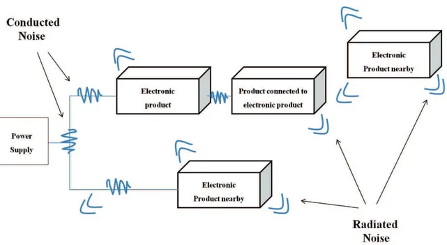
32
Fig. 2.2 Main mode of coupling electromagnetic disturbances: conducted and radiated noise.
In the following we will consider only the conducted emission. The reduction of conducted emissions can also lead to the reduction of any radiated emission, generated by the same currents that travel long conductors, which can act as antennas.
33
2.2 Conducted EMI
Conducted electromagnetic emissions are all the disturbances that propagate through the interconnecting wiring between a device and the network (power cord), or between multiple devices of the same device, or between different devices [18]. From the definition of conducted emissions is possible to highlight two important issues: 1. An external problem that concerns all electromagnetic coupling between the device and the network, or between the system and other systems in the same electromagnetic environment in which it is inserted;
2. An internal problem that concerns the electromagnetic coupling between the different components that make up the apparatus itself.
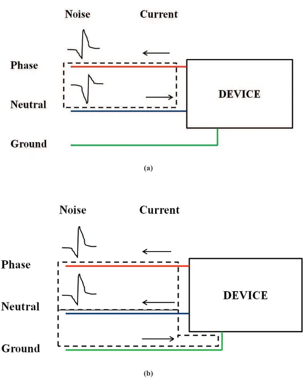
Conducted emissions are generated by two basic mechanisms: differential mode and
common mode. The differential mode interference affecting only the conductors of a
system, while the common mode interference affect all of the conductors and the ground reference. The differential voltage mode (MD) is an electrical potential difference between two conductors junk. This electrical potential difference, originated by the variations of the current required by the load at different frequency from the network, is due to electric currents in the conductors in the opposite direction, for that reason those of MD. There is a common-mode voltage (MC) whenever there is a electrical potential difference between one or more unwanted conductors and the ground reference. This tension, generated by the noise of connections that form common to several circuits (often connections to ground), is due to electric currents in the conductors in the same direction, so said common mode currents [19].
34
(a)
(b)
Fig. 2.3 Conducted Emission: a) differential mode interference: the conductors are affected by the voltage and current of the same magnitude but opposite sign; b) Common mode: the
voltage and current on the phase conductors and neutral have the same sign and the same
magnitude; currents close again through the ground wire.
Conducted noise currents are measured by a spectrum analyzer connected to the LISN (Line Impedance Stabilization Network) placed between the equipment (device) to be
35 tested (EUT, Equipment Under Test) and power source. A typical test configuration is illustrated in Fig. 2.4.
Fig. 2.4 Illustration of the use of a LISN in the measurement of conducted emissions of a product.
The power cord of the product is plugged into the input of the LISN. The output of the LISN is plugged into the commercial power system. AC power passes through the LISN to power the product. A spectrum analyzer is attached to the LISN and measures the “conducted emissions” of the product [16].
The spectrum analyzer measures the amplitude of the disturbance, the variation of frequency, existing between the conductors and the ground reference. It is important that the amplitude of the noise measured on each active conductor does not exceed the limits imposed by the rules for the entire frequency range fixed for the device analyzed.
So that the impedance of the power cord to the outlet of the device under test does not undergo significant variations from site to site and from the same site up changes to the network, you need to input the LISN which makes constant and defined for all the
36 frequencies of the measuring conducted emissions. The LISN also serves to block the conducted emissions in the network supplying the equipment under test, so as not to pollute the measurement made.
2.3 EMC regulations
In the past these issues were usually identified as Electromagnetic Interference (EMI) or Radio Interference (RFI), while currently adopts the name of “compatibility“ that replaces the concept of positive “interference”. The reasons for EMC having grown in importance at such a rapid pace are due to:
1. The increasing speeds and use of digital electronics in today’s world;
2. The virtual worldwide imposition of governmental limits on the radiated and conducted noise emission of digital electronic products.
In 1979 the U.S. Federal Communications Commission (FCC) published a law that placed legal limits on the radiated emissions from and the conducted emissions out the device power cord of all digital devices (devices that use a clock of 9 kHz or greater and use “digital techniques”) to be sold in the USA. Many countries and primarily those of Europe, already had similar such laws in place.
Before the EU directive 89/336/EEC on electromagnetic compatibility and subsequent amendments every country in Europe had its own regulations, which were often at odds with each other. The EU directive 89/336/EEC was subsequently repealed by Directive
37 2004/108/EC, the legislation currently in force, implemented in Italy by Legislative Decree n. 194 of 6 November 2007.
The merit of this work is the standardization of the CISPR (Comité International Special
des Perturbations Radioelectriques), subcommittee of IEC (International
Electrotechnical Commission), international organization that promulgates regulations to
facilitate the trade between the nations. The CISPR is composed of several sub-committees, each of which deals with a specific area as shown in the Table 2.1.
Table 2.1 Classification of CISPR.
In 1985 the CISPR published a set of rules on emissions for ITE equipment, under the title of Publication 22, which is based on Directive 89/336/EEC. The Table 2.2 and the Fig. 2.5 show the limits for conducted emissions of these devices, which are indicated with Class A devices used in domestic and industrial use and Class B with those for private use [16]. As shown above the FCC and CISPR 22 limit on conducted emission extend from 150 kHz to 30 MHz, from 30 MHz to 1 GHz for radiated emission.
38
Table 2.2 Limit of conducted emission of ITE.
Fig. 2.5 Limits of Conducted Emission for ITE Class A and Class B.
At European level the institution with greater technical expertise in this area is the CENELEC (Comité Européen de Normalisation Electrotechnique), which is responsible for collecting and analyzing all national and international standards regarding EMC and remove any technical difference between national standards of member countries.
EU Directive 89/336/EEC and its amendments from 1st January 1996, apply to all electrical and electronic equipment, was subsequently replaced by the current Community legislation, Directive 2004/108/EC. The current Directive states that:
1. The equipment must be constructed in such a way that the electromagnetic disturbance it generates does not exceed a level allowing any other apparatus to function in a manner consistent with their destination;
39 2. The devices have an adequate level of intrinsic immunity to electromagnetic disturbance that would allow them to function in a manner not intended by the manufacturer.
The rules are a real guide, pointing to the measurement mode, the layout and characteristics of the instruments used and the statistical methods for measurements on large scale production. Today the problem of electromagnetic Compatibility regards all the manufacturers of electronic devices whatever their nationality. Currently the companies are very interested to EMC due to the highly competitive nature of the market. In fact, if a device fails the tests for verifying compliance with rules, cannot be sold, even if it is an innovative product. The initial project will therefore have changes such as configuration of the components. All these operations involve an increase in price that can make lasing competitiveness to the product. Also delays the production cycle, caused by the need to solve problems of EMC, can prevent to market the product at the best time, thus leading to declines in sales. On the other hand, device results in a higher profit and a great reputation to the manufacturer.
40
Chapter 3
Power module
3.1 Structure and materials of power modules
As it is mentioned in previous capitals many industrial applications use power modules. The structure of a power module is shown in Fig. 3.1. Power module consist of several semiconductor devices on top of many substrates, such as DBC (Direct Bonded Copper), which are soldered to a base plate.
Fig. 3.1: General design of power module with silicon chip soldered to a ceramic substrates.
Fig. 3.2 shows the structure of a power module with two IGBTs and two diodes in the
most common current technology with substrates made of DCB-ceramics with Al2O3 or
41
Fig. 3.2: Structure of Power Module with two IGBTs and two diodes.
The currently used isolation substrates for power modules are listed in the table 3.1:
Table 3.1: Isolation substrates for power modules.
Isolation material
Ceramic
aluminum oxide Al2O3 aluminum nitride AlN (beryllia oxide BeO)
Organic
Epoxy;
42
Isolation material (Substrates)
Metal Sheets
Direct Copper Bonding);
AMB (Active Metal Brazing).
Metal Sheets IMS (Insulated Metal Substrate) Multilayer-IMS
Thick film layers TFC (Thick Film Copper)
The combination of various materials with a wide range of CTEs (Coefficients of Thermal Expansion) leads to several issues within the assembly, especially the thermal mismatch between the DBC and the base plate or cooler. This is particularly true when these plates are made of conductive metals such as copper or aluminum, as is usually the case.
An important aspect of packaging technology is the selection of material to use for the substrate. Many options are available and selection largely guided by the thermal requirements of the application. The insulating layer between the power semiconductors and the heatsink is a substrate, which can be of different technology, such as: DBC (Direct Bonded Copper), AMB (Active Metal Brazed), IMS (Insulated Metal Substrate) and TFC (Thick-Film-Copper).
The most widespread substrate is Al2O3 ceramic. Over the past few years the thickness of this substrate was reduced from 0.63 to 0.38 mm for a number of applications to reduce the thermal resistance (Rth) of the chip to the heat sink [20].
43
Fig. 3.3: Typical thicknesses of the layers.
A DBC substrates consists of a layer of ceramic insulator bonded between two layers of copper, providing electrical insulation and excellent thermal path to a single heatsink [21] (see Fig. 3.4 and Fig. 3.5).
Direct bonded copperis composed of a ceramic tile with a sheet of copper bonded to one
or both sides by a high-temperature oxidation process.
Ceramic material used in DBC include:
· Alumina (Al2O3), which is widely used because of its low cost. It is however not
a really good thermal conductor (24-28 W/mK) and is brittle;
· Aluminium nitride (AlN), which is more expensive, but has far better thermal
performance (> 150 W/mK);
· Beryllium oxide (BeO), which has good thermal performance, but is often
avoided because of its toxicity when the powder is ingested or inhaled.
With its good thermal conductivity and excellent dielectric properties, the ceramic layer within the DBC provides the silicon chips the essential electrically isolated thermal path with negligible impact on the overall thermal performance of the assembly [21]. For this reason DBC substrates are commonly used in power modules.
44
Fig. 3.4: Profile of DBC substrate show electrical isolation and low thermal resistance.
Fig. 3.5: Structure of a DBC.
The bottom side of the DCB-ceramic substrate is fixed to the module base plate by soldering, see Figure 3.6 and Fig. 3.7.
45
Fig. 3.6: Views of power module.
Advantages of the DCB-technology compared to others are: · high current conductivity due to the copper thickness; · good cooling features due to the ceramic material;
· the high adhesive strength of copper to the ceramic (reliability);
· the optimal thermal conductivity of the ceramic material [7],[22].
The AMB process (“brazing” of metal foil to substrate) has been developed on the basis of DCB technology. The advantages of AMB-substrates with AlN-ceramic materials compared to substrates with Al2O3-ceramic materials are e.g. lower thermal resistance,
46 lower coefficient of expansion and improved partial discharge capability. Figure 1.43 explains the differences between DCB and AMB.
The IMS (Insulated Metallic Substrate) is a doped polymer covered on one or both sides by a thin copper layer. IMS is used in power conversion, motor drivers, solid state relays and welding machines. IMS substrates have relatively high coefficients of thermal expansion and thus limited temperature stability and cycle life, while the coefficients of thermal expansion in DBCs are similar to silicon. Whereas IMS have low current carrying capacity, DBCs offer high current carrying capacity. Both substrates exhibit good heat dissipation. The main function of the base plate is as a mechanical support for the system whilst also transferring the heat, primarily via conduction, to the heatsink. When the passive cooling is insufficient, then base plates with larger surface areas can be utilized in active cooling. The thermal grease between the chip and the heatsink limits the thermal dissipation and induces temperature in-homogeneity. Aluminum wire bonding limits the current capability and fuse with high current leading to catastrophic failures [23]. Aluminum wire bonding are used to interconnect the emitter and gate pads from the device to the outside leads. One fundamental difference between power modules is that they are designed either with or without a base plate. In modules with no base plate the DBC substrate is mounted directly onto the heat sink (Fig. 3.7).
47 Such modules are characterized by the use of few large chips with good heat spreading through the base plate:
Advantages:
· Mechanically more robust during transport and assembly;
· Larger thermal mass, lower thermal impedance within the range of 1 s.
Disadvantages of modules with soldered or bonded chips (IGBT modules):
· Higher thermal resistance chip because base plate bending requires a thicker layer
of thermal paste;
· Reduced slow power cycling capability, since the large-area base plate solder
pads are susceptible to temperature cycles;
· Higher internal terminal resistances, since, for thermo-mechanical reasons, the
design is based on small ceramic substrates that require additional internal connectors;
· Increased weight.
Such modules use smaller chips and achieve thermal spreading on the heat sink thanks to heat sources which are better spread.
Advantages:
· Lower thermal resistance because layers are omitted, even contact with the heat
sink results in thinner thermal paste layers;
· Improved thermal cycling capability; because of removal of solder fatigue in base
48
· Smaller chips; lower temperature gradient over the chip means a lower maximum
temperature and less stress under power cycling conditions;
· Few large ceramic substrates with low terminal resistance.
Disadvantages:
· No heat storage;
· Processable chip size is limited, resulting in more parallel connections;
49
Chapter 4
Numerical methods in electromagnetism and
simulation tools
4.1 Generality on numerical methods
The resolution of the problems of the electromagnetic type, as it is the case for several other scientific fields, can be addressed with analytical methods as long as the system does not present a high level of complexity. In fact, otherwise, when the geometries are no longer simple and regular, it becomes much more difficult the resolution of the differential equations that govern it, and then it is necessary adopt methods based on numerical techniques. The most widely used for the calculation of the electromagnetic fields are:
1. Finite Element Method (FEM);
2. Partial Element Equivalent Circuit (PEEC);
3. Method of Moment (MOM).
The idea behind is to calculate the value of the variables you want only at certain points of the domain of interest, transforming the differential equations that describe the problem in algebraic equations approximate, and respecting the boundary and initial conditions.
50 In the following there is a more detail description of the three methods and tools used for the analyses.
Table 4.1: Main features of the most common EM simulation techniques.
Method FEM MoM PEEC
Formulation Differential Integral Integral
Solution variables Field Circuit Circuit
Solution domain TD or FD TD or FD TD and FD
Cell geometries Nonorthogonal Nonorthogonal Nonorthogonal
Advantages Cell flexibility Complex materials
Cell flexibility Same TD/FD model Comb. Circuit & EM Cell flexibility
51
4.2 Finite Element Method
4.2.1 Generality
The FEM (Finite Element Method) is one of the most widely used numerical techniques that allows to obtain approximate solutions to problems described by equations partial differential equations (PDEs). Originally, the FEM was developed by engineers for the mechanical calculation of structural elements. Today it is widely used in many areas both of scientific world and of industry, to make accurate modeling of various phenomena in the field of electromagnetism, structural and thermal analysis, fluid dynamics and also in problems so-called " Multiphysics " where you have to solve systems of coupled differential equations. It is possible to split the FEM in three main phases:
1. The first phase consists of the subdivision of the problem domain in subdomains called finite elements. In the case of the two-dimensional problems finite elements are usually triangles or quadrangles, similarly, in the case are three-dimensional tetrahedrons or parallelepipeds. Due to their better
adaptability triangles and tetrahedrons are used more frequently.
The set of the totality of all these elements is called a mesh.
2. The second phase is the translation of a BVP (Boundary Value Problem) in a system of linear equations algebraic. The two most common ways to get this system are the minimization of a functional, generally representing the energy of system and the variational methods as one of weighted residues of Galerkin.
52
Fig. 4.1 Boundary Value Problem.
In each finite element, the solution (eg. a electromagnetic variable) is approximated by a series of simple functions called shape functions, associated to the degrees of freedom (DOF - degrees of freedom) of the problem. The degrees of freedom are often geometrically associated with both the vertices with both finite element interior points called nodes.
3. Finally, the equations of the different elements are assembled into a global system of linear equations algebraic, which resolved, in the third phase, known as post-processing, enable to perform the processing and interpretation of the results of the solution of the system of equations.
53
4.3 FEM and electromagnetism
4.3.1 Finite Elements and shape function
In this section some aspects of problems in electromagnetic field are presented. In scalar problems the field is calculated in the nodes and unknown approximate function is
obtained by interpolating the nodal values by scalar functions
a
( )
rr)
. The variable field Vat each point of a finite element can be expressed as:
( )
( )
1 N i i iV r
V
a
r
==
å
)
N( )
r
)
å
V
iii iii(
r
(4.1) where:- N is the number of nodes of the element; - Vi is the value of V to node i.
In the two-dimensional case, at any point r=
(
x y,)
internal a triangular element (Fig. 4.2) the linear shape functiona( )
rr is defined as:)
( )
i i A r A a)
= Aiii r = (4.2)where Ai is the area of a element section and A is the total area of the element (see Fig.
54
Fig. 4.2 Triangular Finite Element.
Considering i=1, 2,3, Ai and A can be calculated as follows expressed:
1 1 2 2 1 1 1 2 1 i i i i i x y A x y x y + + + + æ ö ç ÷ = ç ÷ ç ÷ è ø 1 1 2 2 1 1 1 2 1 i i i i x y A x y x y + + + + æ ö ç ÷ = ç ÷ ç ÷ è ø (4.3)
The functions ai
( )
rr)
are called Lagrangian and fulfill the followingrelations:
( )
3 1 1 i i r a = =å
r =)
1 (4.4)( )
i j 1 if α r = 0 otherwise i= j ì í î)
1 if r)
= i j i j i ì í ìì (4.5)55 For three-dimensional problems in the time or frequency domain, it is generally necessary to use a vector variable. With a such as variable we
can rewrite the expression (4.6) using the same shape function
present in (4.1):
( )
( )
1 N i i i U r Ua r = =å
(
U r(
r))
Uiiii iiii(
( )
r)
N U(
r r)
å
(4.6)where UUi is the unknown nodal vector in the i-th node that is to say, we have 3N scalar coefficients.
Equation (4.6) can be used only if the unknown vector variable is continuous throughout the entire domain of the problem as in the case of vector potential AA when it is used for
the solution of problems eddy current. In fact, if we consider a region in which you want to calculate the electric field vector EE or the magnetic field vector HH , characterized by
material inhomogenities, the normal component of these vectors will be discontinuous at the interface between the different materials. Similarly, if in the same region you want to determine the vectors DD or BB , will be the tangential component to be discontinuous at
the interface.
In these cases the (4.6) is inappropriate and should be used an expression that takes account of these discontinuities. Below is the equation (4.7) that makes use of the vector function ww:
( )
( )
1 N i i i U r U w r = =å
(
U r(
r))
U w rii ii( )
(
N r)
å
(4.7)Given a 3D mesh consists of elements of tetrahedral shape (Fig. 4.3), it is possible to associate a vector shape function wwiii to every edge of a tetrahedron.
56 By performing the dot product between the function wwiii constant and the vector lying
along the edge of the tetrahedron eeii with i=1, 2,..., 6 we obtain the following
relationship:
i j ij
e wi× j =dij
e wiiii wwjjjj =diiii (4.8)
where dij is the Kronecker symbol.
Fig. 4.3 Tetrahedron Element.
If for every element of tetrahedral shape the unknown function UU is approximated
through function wwiii we obtain:
( )
6( )
1 i i i U r U w r = =å
(
U r(
r))
U w rii ii( )
(
6 r)
å
(4.9)The integral linear UU along the edge of the tetrahedron eeii is: 1 ˆ i i i i e U U t dl L =
ò
× i i i eò
i i i U t dlUU ˆˆi (4.10)57
4.3.2
The equations of the electromagnetic field
The study of all electromagnetic problems is based on Maxwell's equations, which describe the phenomena of interaction between the electric and magnetic fields. These are four partial differential equations and have the following form:
F D
r
Ñ× = F Dr
F Ñ× =D (4.11) 0 B Ñ× = 0B Ñ× =B (4.12) B E t ¶ Ñ´ = -¶ B E ¶BB Ñ´ = -E B (4.13) D H J t ¶ Ñ´ = + ¶ D H J ¶DD Ñ´HH = +JJ D (4.14) where: DD is the electric induction C/m2;
B
B is the magnetic induction Wb/m2;
E
E is the electric field V/m;
H
H is the magnetic field A/m;
F
r is the free electric charge C/m3;
JJ is the density of electric current A/m2.
The electrical and magnetic induction vectors depend on the respective fields as indicated in the following constitutive relations that, in the simplifying assumptions of isotropic, linear and non-dispersive media takes the form:
58
D=
e
ED EEE (4.15)
B=mH
B HHH (4.16)
being
e
and m the electrical and magnetic permeability respectively. The currentdensity JJ is related to the electric field EE and current source JJs by the following equation:
s
J =
s
E+JJ EEEEE J (4.17)
where
s
is the electric conductivity of the material.Applying the divergence to both sides of (4.14) is obtained by the equation of continuity given by: 0 D J t æ ¶ ö Ñ ×ç + ÷= ¶ è ø ö D D D =öö D J + D J Döö J ¶D öD (4.18)
Starting from Maxwell's equations and the constitutive equations can be
obtain different formulations for solving problems based on fields or
potential, with one or more unknown variables. Moreover, in any case, it is necessary to impose the boundary conditions (typically Dirichlet or Neumann ones) on the surface of domain in which the problem of the electromagnetic field must to be solved;
since, usually, the surfaces coincide with the boundary surfaces of
separation between different mediums, the boundary conditions are imposed taking into account of the equations of the fields at the interface between two media with properties different physical.