STRUCTURAL, FERROELECTRIC AND PIEZOELECTRIC
PROPERTIES OF
EPITAXIAL PMN-PT THIN FILMS
DEPOSITED BY PULSED LASER DEPOSITION
Doctorate studies have been performed under guidance of
Supervisor: Prof. dr. ing. Edoardo Bemporad
Materials Science and Technology Group (STM)
Engineering Department: Mechanical and Industrial Engineering University of Rome "ROMA TRE" 00146 Rome, Italy
Supervisor: Prof. dr. ing. A. J. H. M. Rijnders
Inorganic Materials Science Group (IMS) MESA+ Institute for Nanotechnology Faculty of Science and Technology
University of Twente, 7500 AE Enschede, The Netherlands
Assistant Supervisor: Dr. ing. Giulia Lanzara
Materials Science and Technology Group (STM)
Engineering Department: Mechanical and Industrial Engineering University of Rome "ROMA TRE" 00146 Rome, Italy
PhD studies have been accomplished at
Materials Science and Technology Group (STM)
Engineering Department
Section: Mechanical and Industrial Engineering University of Rome "ROMA TRE" 00146 Rome, Italy
Inorganic Materials Science Group (IMS)
MESA+ Institute for Nanotechnology Faculty of Science and Technology
Thesis Commission Members: Full Members (Membri effettivi)
Prof. dr. ing Ennio Antonio Carnevale University of Florence, Florence, Italy Prof. dr. ing. Giancarlo Chiatti
University of Rome “Roma Tre” Rome, Italy Ass. Prof. dr. ing. Fabio Giulii Capponi University of Rome “La Sapienza” Rome, Italy
Experienced Members (Membri Esperti)
Dr. ing. Uwe Schulz
German aerospace centre, Köln, Germany Dr. ing. Francesco Salvatore
CNR, Italy
This dissertation to be publically defended on 12th of June 2014 at 10:00 am.
Financial Support:
The research work reported in this dissertation has been financially supported by the Engineering Doctorate School of University of Rome "ROMA TRE" and by NanoNextNL, a micro and nanotechnology consortium of the Government of the Netherlands and 130 partners.
Abstract
Ferroelectric oxides, most notably PZT, are typically used for the fabrication of high performing piezoelectric MEMS devices for the purpose of sensing and actuation. An alternative to PZT is the relaxor ferroelectric such as PMN-PT. Bulk PMN-PT shows a 5-10 times larger piezo-response than bulk PZT ceramics and has a large electromechanical coupling coefficient of k33≈0.9.
Therefore, this material is an auspicious candidate for hyperactive MEMS devices for sensor and actuator applications. This thesis deals with the study of epitaxial PMN-PT films for the purpose of sensing and actuation.
Perovskite phase and (001) orientation pure epitaxial PMN-PT films were fabricated by carefully controlling the fabrication conditions. Within a relative narrow process window to achieve phase and orientation pure films, the effect of the growth conditions like substrate temperature, fluence, target-substrate distance and ambient gas pressure was investigated. This study shows that polarization is more sensitive to substrate temperature then to target distance and much less to fluence and least to gas pressure.
It is known that better lattice matching can broaden the processing window. Superior lattice matching was achieved using a PZT buffer layer between the PMN-PT and SRO bottom electrode resulting in a significant improvement in crystallinity and consequently in properties of the PMN-PT films. Furthermore the effect of lattice strain was investigated by varying the PZT interfacial layer composition in a wide range. The PMN-PT films showed giant self-bias field which can be tuned by the composition the of PZT interfacial layer. This is of significance for devices like energy scavengers and low energy consumption sensors that preferably operate at zero bias voltage.
The highest longitudinal piezoelectric coefficient (d33) was achieved for
PMN-PT films deposited on PZT (50/50) interfacial layer with lowest self-bias field. For some applications, it is desirable to have a higher d33 as well as a high self-bias.
It is known that doped PZTs can produce self-bias field. Therefore, PMN-PT films were deposited on Nb and Fe doped PZT interfacial layers. PMN-PT films on doped PZT interfacial layer show a higher self-bias along with a higher d33. Furthermore
the effect of Nb-doped PZT interfacial layer thickness on the properties of PMN-PT was investigated, which showed a variation in properties associated with epitaxial strain.
Besides epitaxial strain, the residual strain (substrate induced strain) due to the difference of thermal expansion coefficients between substrate and deposited film, show an influence on the ferro and piezoelectric properties of epitaxial PMN-PT films. To study the effect of substrate induced strain on the ferro and piezoelectric properties, PMN-PT films were prepared on a wide range of substrates. This study shows that substrate induced strain has a significant effect on the
structural properties of PMN-PT films and consequently on the ferro and piezoelectric properties of these films. The knowledge of strain effect on properties is useful to engineer a PMN-PT film with certain desired properties.
Silicon is the gold standard substrate for the fabrication of MEMS sensors. To study the effect of orientation on properties, epitaxial PMN-PT films with different out of plane orientation [(001) and (110)] were prepared using a CeO2/YSZ
bilayer buffer and symmetric SrRuO3 electroded silicon substrates by carefully
controlling the growth conditions. The ferroelectric and piezoelectric properties of these ferroelectric capacitors exhibited orientation dependence. The (001) oriented films show a relatively large self-bias voltage compared to the (110) oriented films. This is ascribed to a strain gradient layer in the relaxor at the interface with the bottom electrode. The aging behaviour of (001) films was superior compared to that of (110) films due to less structural defects. Nevertheless a superior effective, longitudinal piezoelectric coefficient (d33,eff) for (110) oriented films was observed
compared to (001) oriented films, due to a less dense columnar structure. Furthermore, a PMN-PT thin film based sensing device (cantilever) was also fabricated and characterized with respect to ferroelectric and piezoelectric response which showed excellent properties.
All praises for Allah who is the entire source of knowledge and wisdom endowed to mankind
and
all respect for The Holy Prophet (PBUH) who is forever a torch of guidance
Table of contents
Chapter 1. Introduction
1.1 Overview of ferroelectric materials 2
1.2 Epitaxial thin films and misfit strain 4
1.3 Thin film nucleation and growth 5
1.4 Ferroelectric fundamentals 7
1.5 Relaxor and standard ferroelectrics 9
1.6 Thesis outline 12
1.7 References 13
Chapter 2. Fabrication and Characterization
2.1 Introduction 172.2 Thin films fabrication by Pulsed Laser Deposition 17
2.2.1 Principle of PLD system 17
2.2.2 PLD system structure 18
2.2.3 Epitaxial PMN-PT heterostructures 21
2.2.4 Device design for analysis 22
2.3 Characterization techniques 24
2.3.1 Structural analysis 24
2.3.2 Microstructure and morphological studies 25
2.3.3 Electrical investigations 28
2.3.4 Electromechanical investigations 31
2.4 References 33
Chapter 3. Processing of PMN-PT films
3.1 Introduction 363.2 Experimental procedure 39
3.2.1 Samples fabrication 39
3.2.2 Samples characterization 40
3.3 Results and discussions 40
3.3.1 Phase optimization and structural properties 40
3.3.2 Ferroelectric and piezoelectric properties 44
3.3.3 Surface morphology and microstructure 49
3.4 Conclusions 50
3.5 References 51
Chapter 4. PMN-PT films on PZT interfacial layer
4.1 Introduction 544.2 Experimental procedure 55
4.2.1 Samples fabrication 55
4.2.2 Samples characterizations 56
4.3 Results and discussions 57
4.3.1 Structural properties 57
4.3.3 Dielectric and piezoelectric properties 69
4.4 Conclusions 71
4.5 References 72
Chapter 5. PMN-PT films on doped PZT interfacial layer
5.1 Introduction 755.1.1 Hard verses soft doped PZTs 75
5.1.2 Iron and Niobium doped PZTs 77
5.2 Experimental procedure 79
5.2.1 Samples fabrication 79
5.2.2 Samples characterization 80
5.3 Results and discussions 81
5.3.1 Structural properties 81
5.3.2 Ferroelectric and piezoelectric properties 83
5.3.3 Ferroelectric response stability behaviour 86
5.4 Effect of Nb-PZT layer thickness on PMN-PT properties 87
5.4.1 Structural properties 88
5.4.2 Ferroelectric and piezoelectric properties 91
5.4.3 Ferroelectric response stability analysis 93
5.5 Conclusions 94
5.6 References 95
Chapter 6. Substrate induced strain in PMN-PT films
6.1 Introduction 996.2 Substrates and substrate pre-treatments 102
6.3 Experimental procedure 103
6.3.1 Samples fabrication 103
6.3.2 Samples characterization 104
6.4 Results and discussions 104
6.4.1 Structural properties 104
6.4.2 Ferroelectric and piezoelectric properties 109
6.5 Conclusions 112
6.6 References 113
Chapter 7. Integration with silicon
7.1 Introduction 1167.2 Orientation control of PMN-PT films [(001) and (110)] 118
7.2.1 Thin films growth 118
7.2.2 Thin films characterizations 119
7.2.3 Results and discussions 120
7.3 Fabrication of PMN-PT film based free standing cantilever 129
7.3.1 Deposition of PMN-PT films stack for cantilever beam 129
7.3.2 Structure, ferroelectric and piezoelectric characterization 130
7.3.3 Structural properties of PMN-PT films stack 130
7.3.4 Fabrication process of free standing cantilever 131
7.5 References 135 Acknowledgements 137 List of Publications
139
1.
Introduction
Chapter Overview:
This chapter describes brief history of ferroelectric materials together with evolution of ferroelectric technology. Nucleation and growth of epitaxial thin films along with hetero-epitaxy induced strain and strain relaxation by structural defects is briefly explained. The material used in this dissertation is a solid solution of relaxor and standard ferroelectric. The fundamentals related with relaxors and standards ferroelectric are also presented. The last part of this chapter describes the outline of this thesis.
1.1 Overview of ferroelectric materials
An unusual physical characteristic to attract the other objects when heated was observed in tourmaline during the beginning of the 18th century. About half a century later, a Swedish scientist Carl Linneaus speculates a correlation between this observed phenomenon and electricity. This speculation was confirmed and the effect named pyroelectricity within a decade by a German Physist Franz Aepinus. Pyroelectricity refers to the ability of a material to generate temporary voltage while heating or cooling [1]. In 1880, pyroelectricity led to the discovery of the piezoelectricity by Piere Curie and Jacques Curie. They observed that certain materials (Tourmaline, Quartz, Cane sugar and Rochelle salt) exhibit charge generation on application of mechanical stresses on their surfaces. They applied mechanical stress by placing small weights on the surface of the crystal and found that the magnitude of the generated charge is proportional to the applied stress [2]. The German Physicist Wilhelm G. Hankel introduced the term piezoelectricity derived from ancient Greek words piezo or
piezein (pressed or squeezed) and elektron (Amber: ancient source of
electric charge). The inverse piezoelectric effect was proposed by French Physicist Gabriel Lippmann and was experimentally verified by the Curie brothers in the same year [1]. Direct and inverse piezoelectric effect is schematically described in figure 1.1.
Figure 1.1: Schematic description of the direct and inverse piezoelectric effect.
In 1920 Valasek found that the direction of polarization can be reversed in Rochelle salt (KNaC4H4O6٠4H2O) by applying external electric field. The phenomenon is called ferroelectricity. This was the first discovered ferroelectric material [3]. This material was entitled ferroelectric due to the occurrence of spontaneous polarization which is analogous to spontaneous magnetization in ferromagnetic materials.
It is notable here that although the prefix ferro is used, most of the ferroelectric material do not contain iron. Subsequently potassium di-hydrogen phosphate (KH2PO4) having similar properties to Rochelle salt was reported in 1935.
It was common believe that a hydrogen bond is necessary for a material to possess ferroelectric properties until Wul and Goldman identified the presence of ferroelectricity in barium titanate (BaTiO3) in 1945 [4]. This was the first oxide material with perovskite crystal structure showing ferroelectric behavior. This discovery initiated the curiosity to search for ferroelectricity in oxide materials. Due to structural simplicity, chemical and mechanical stability, ferroelectricity at room temperature and simplicity in fabrication, BaTiO3 is included in the list of the highly investigated/used ferroelectric materials. During this era numerous ferroelectric oxide materials with perovskite structure like KNbO3, KTaO3, LiNbO3, PbTiO3 were discovered [5-8].
The struggle to fabricate better and better ferroelectric materials resulted in the discovery of lead zirconate titanate (PZT) in the 1950s [9]. PZT is a solid solution of PbTiO3 (PTO) with PbZrO3 (PZO). Due to its superior properties compared to BaTiO3, this material has replaced it in almost all its piezoelectric applications. To date, this material is the most widely employed piezoelectric material due to its superior properties and relatively high Curie temperature.
In 1997, S. E. Park and T. R. Shrout reported PZN-PT and PMN-PT single crystal ceramics with ultrahigh strain up to 1.7% and large electromechanical coupling coefficient of k33≈ 0.9. These materials show one order of magnitude superior piezoelectric response compared to PZT due to electrical field induced phase transitions from rhombohedral to tetragonal phase. Subsequently giant piezoelectricity was reported by S. H. Baek et al. for epitaxial PMN-PT thin films deposited on silicon substrate in 2011[10-11]. This material got huge interest to fabricate hyperactive MEMS devices in recent years. Further details about epitaxial PMN-PT films will be discussed in chapter 4.
1.2 Epitaxial thin films and misfit strain
Epitaxy is derived from two ancient Greek words epi (placed or resting upon) and Taxis (arrangements). During thin film growth, epitaxy refer to extended single crystal film formation on top of a single crystal substrate. It was most likely first observed to take place in alkali halide crystals over a century ago [12]. The word Epitaxy was apparently introduced by French mineralogist L. Royer in 1928 [13].
Epitaxy can be divided into two types, homo-epitaxy and hetero-epitaxy. Homo-epitaxy refers to the situation when fabricated film and substrate are of the same material. For instance, epitaxial growth of silicon thin film on top of the single crystal silicon substrate. Under optimum conditions, homo-epitaxial layers possess generally less structural defects compared to the substrate, purer than substrates with doping possibility independent of the substrate [12]. On the other hand, hetero-epitaxy refers to the situation when the deposited film and the substrate consist of two different materials. For example, epitaxial growth of SrRuO3 on top of the SrTiO3 single crystal substrates. Hetero-epitaxial growth of functional materials is commonly performed for the fabrication of electronics, photonics and MEMS (micro electromechanical systems) devices. The difference between homo-epitaxy and hetero-epitaxy is schematically demonstrated in figure 1.2.
Figure 1.2: Schematic view of the lattice matched or homo-epitaxial structure
When the deposited film and the substrate crystal are identical (Homo-epitaxy), there is no bonding strain at the interface due to perfect lattice matching. However in the hetero-epitaxy case, the lattice parameters are not identical. The lattice mismatch can be defined as (equation 1.1).
ℎ = 1.1
Where af and as are lattice parameters of the film and substrate respectively. The lattice mismatch plays a crucial role during hetero-epitaxial growth of functional thin films. In case of very small mismatch (≤ 1%) between film and substrate, the hetero-interface is essentially similar to homo-epitaxy. Nevertheless the difference in thermal expansion coefficients and film-substrate chemistry can still strongly influence the functional properties of the deposited film. In case of relatively large lattice mismatch (≥ 5%), crystallographic lattice mismatch is either accommodated by the formation of structural defects (edge dislocations) or by tensile/compressive lattice strain at the interface. The strain relaxation by structural defects where the film reflects the bulk lattice parameters is referred to as relaxed epitaxy. The latter case, where the film is strained to the substrate is referred to as strained epitaxy. Strain epitaxy is mainly observed in the hetero-epitaxial layer of similar structure like perovskite SrRuO3 on top of perovskite SrTiO3 single crystal substrate.
1.3 Thin films nucleation and growth
Interests in thin film fabrication exists since the 1920s from the experiments performed on evaporated films in Cavendish laboratory in Cambridge, England [14]. At earliest stage of thin film fabrication, adatoms (adatoms refer to the atoms that reach to the substrate surface from the source) with sufficient energy reach the substrate and form clusters as a result of diffuse process on the substrate surface. These clusters become stable after a certain critical thickness. The process of formation of the stable clusters is called nucleation. Many of such
events take place simultaneously at the nucleation stage. As growth continues, coalescence of the stable clusters results in continuous film on the substrate surface. Three growth modes are typically observed during thin film growth.
1. Layer by Layer growth or Frank-van der Merwe mode 2. Island growth or Volmer-Veber mode
3. 2D followed by 3D growth or Stranski-Karastanov mode
In layer by layer growth mode, the smallest stable cluster coalesce in two dimensions only to form planner sheets. During growth, subsequent layers only nucleate with the completion of the underneath layer. In this growth mode, adatoms are more strongly bound to the substrate compared to one other which promotes the layer by layer growth.
In island growth mode, stable clusters nucleate on the substrate surface which only grows in three dimensions to form islands. In this case, adatoms are more strongly bound to each other as compared to the substrate which facilitates the formation of 3D islands.
The Stranski-Krastanove growth mode is a combination of above two modes. Initially films grow in layer by layer mode followed by transition to three dimensional mode. Due to lattice mismatch, strain energy accumulates in the films. After certain critical thickness, the system releases its energy by triggering the island growth mode.
Besides this, another growth mode (step flow) is also reported in the literature [15-16]. This mode differs from layer by layer growth mode in the sense that it occures only in one direction on the terraces of low miscut angle substrates. Three basic growth modes are schematically shown in figure 1.3.
1.4 Ferroelectric fundamentals
The family of materials that possess spontaneous polarization whose direction can be reversed by applying external electric field are said to be ferroelectric materials [17]. The relationship between ferro, pyro and piezoelectric materials is schematically shown in figure 1.4. It is evident from this correlation that all ferroelectric materials are both pyroelectric and piezoelectric and all pyroelectric materials are piezoelectric [18]. For instance, PMN-PT possesses spontaneous polarization and is ferro, pyro and piezoelectric simultaneously, whereas Tourmaline does not possess spontaneous polarization, is not ferroelectric, but is pyro and piezoelectric.
Figure 1.4: Relationship between ferro, pyro and piezoelectric materials.
Crystalline materials can be categorized into seven basic crystal systems; i.e. triclinic, monoclinic, orthorhombic, tetragonal, rhombohedral, hexagonal and cubic. These can be further divided into 32 sub-classes termed as point groups. Twenty point group out of all 32 groups are non-centro-symmetric and exhibit piezoelectric behaviour which is a pre-condition for this. Out of twenty piezoelectric point groups, half exhibit single polar axis and are pyroelectric with temperature dependence. The materials that do not show spontaneous polarization are termed as non-polar or para-electric [19]. It is valuable to mention here that symmetry considerations are helpful to predict whether a material possesses such
a property (Ferro, Pyro, Piezo) or not. Nevertheless this does not give any information about quantification of any specific property. Parameters like fabrication conditions, density, crystal structural etc. can influence the properties significantly.
Superior properties has been reported for the inorganic ferroelectric oxides like BaTiO3, BiFeO3, Pb(ZrxTi1-x)O3 and Pb(Mg1/3Nb2/3)O3-PbTiO3. These materials belong to the perovskite family and can be described with general formula ABO3. Perovskites are refer to the catagory of materials that have crystal structure similar to CaTiO3,discovered by Gustave Rose in 1839 and named perovskite after Count Lev Alekseevich Perovski, a Russian mineralogist [20]. When the unit cell of the perovskite material is cubic, then the atom A will assemble itself at the corner position of the cube. The atom B and O (oxygen) will reside in body centre and face centre positions of the cube respectively. PMN-PT is a perovskite material with one A site cation and three B site cations. Lead is located at position A whereas other three (Mg, Nb, Ti) are located at position B. The B site cations are randomly distributed inside the material. The oxygen will occupy at face center of the cube. The perovskite unit cell is schematically shown in figure 1.5.
Figure 1.5: Schematic view of perovskite unit cell with atomic locations.
Ferroelectric materials show a paraelectric to ferroelectric phase transition at a specific temperature. This transition temperature is named as Curie temperature (Tc). Above Curie temperature (paraelectric phase), the unit cell is centro-symmetric and does not exhibit spontaneous polarization. Upon cooling (below Tc), it adapts
the ferroelectric phase. The symmetry of the unit cell also changes from centro-symmetric structure to non-centro-symmetric structure. Inside the perovskite unit cell, the central ion moves from its equilibrium position within the oxygen octahedra. Consequently the material transforms from paraelectric phase to ferroelectric phase [21]. Functional ferroelectric material (PMN-PT) discussed in this dissertation retains cubic crystal structure (paraelectric phase) above Curie temperature. Bellow Curie temperature, it adopts tetragonal or rhombohedral crystal structure (ferroelectric phase) as a consequence of structural transformation from the cubic structure. It is worth to mention here that there is a composition dependent border line separating tetragonal from rhombohedral crystal structure below Curie temperature named as morphotropic phase boundary [22]. The direction of polarization in tetragonal and rhombohedral crystal structure is along <001> and <111> respectively. The polarization refers to the total dipole moment (μ) per unit volume (V) and can be written as
= 1.2
Typically in ferroelectric materials, the polarization is not uniformly aligned in the same direction inside the entire crystal. The region inside the crystal in which spontaneous polarization is aligned in one direction is named as domain. The interface separating two domains is called domain wall. The non-uniformly aligned polarization in bulk ferroelectric materials can be aligned by applying external field named as poling process. However, the poling is not needed for epitaxial films due to self-alignment of the domains during fabrication.
1.5 Relaxor and standard ferroelectrics
Lead magnesium niobate - Lead titanate (PMN-PT) reported in this dissertation is a solid solution of lead magnesium niobate (PMN) and lead titanate (PT). The PbMg1/3Nb2/3O3 (PMN) is a classical relaxor having cubic crystal structure at high temperature and pseudo-cubic at lower temperature [23]. The PbTiO3 (PT) is a typical ferroelectric material that shows cubic structure above Curie
temperature (Tc ≈ 770K) and tetragonal below Tc [24]. The relaxors can be distinguished from normal ferroelectrics in terms of properties summarized in table 1.1.
Table 1.1: Property difference between relaxor and normal ferroelectric (Table adopted from reference 25).
Properties Normal Ferroelectric Relaxor
Dielectric temp. dependence
K = K(T)
Sharp 1st or 2nd order
transition about Curie temperature (Tc)
Broad diffuse phase transition about Curie
Maxima (Tmax)
Dielectric temp. and freq. dependence K = K(T, ω) Week frequency dependence Strong frequency dependence Dielectric behavior in paraelectric range (>Tc)
Fellow Curie-Weis law
1 K=
C T − Tc
Fellow Curie-Weis square law 1 = 1 + − 2 Remanent Polarisation (Pr) Strong remanent Polarisation (Pr) Weak remanent Polarisation (Pr) Scattering of light Strong anisotropy
(birefringent, ∆n)
Very weak anisotropy to light (pseudo-cubic) Diffraction of X-rays
Line splitting indicating spontaneous deformation (paraelectric→ferroelectric
phase)
No X-rays line splitting giving a pseudo cubic
structure
Relaxor (PMN) typically exhibit diffuse phase transition with significant dispersion (temperature and frequency dependent) in dielectric permittivity. Secondly, low temperature behavior under high alternating fields exhibit unpretentious hysteretic response, a necessary and sufficient condition for ferroelectricity. Nevertheless, unlike a normal ferroelectric, the hysteretic response is not lost suddenly at Tmax but decays more slowly in a nonlinear mode. Moreover relaxors exhibit longer coherence length while probing with radiations (light, X-rays) i.e. no evidence of optical anisotropic or x-rays line splitting even well below Tmax. The model proposed by Smolensky suggests that the origin of diffuse phase transition is due to
local compositional fluctuations associated with B-site cation disorder, resulting in a distribution of Curie temperatures [23]. Subsequently Cross proposed a super-paraelectric model suggesting that the existence of localized polar micro-regions which are analogous to spin clusters behavior in super-paramagnets. This model successfully explains properties like frequency dependence of the permittivity, dielectric aging, and metastable switching from micro to macro domains in relaxors [25-26]. The clear evidence of nonpolar region (NPRs) came from refractive index measurement experiments performed by Burns and Dacol. They reported the formation of static or slowly moving nanopolar-regions (PNRs) about 620K having a size of a few nm. This temperature is refered to as Burns temperature (TB) [27-28]. Subsequent studies performed by different techniques (X-rays, neutrons scattering, HR-TEM etc.) shows consensus about PNRs which begin to appear at 618K which grow 2-3nm in size near TB. Further cooling up to 160K enhances the size (≈10nm) and volume fraction increases upto 30 percent. A static change in NPRs can be induced by high electric field and micro domains can be obtained which lead to the observation of ferroelectricity at lower temperatures [29-32].
A crystalline solid solution [(1-x)PMN-(x)PT] is shown to be possible over a whole range of concentrations of x [33]. Colla et. al. studied the frequency dependence of dielectric permittivity for wide range of PMN-PT compositions and found that above x ∼ 0.3 the value of Tmax becomes frequency independent. These investigations suggest that for PT concentrations higher than ∼0.3, the phase transformation becomes largely like a conventional ferroelectric phase transition [34]. Xu et.al. investigated the PMN-PT (67:33) single crystals and found the co-existence of monoclinic and rhombohedral phase, in the same single crystals. They suggested that electric field induced polarization rotation takes place via rhombohedral-monoclinic-tetragonal phase transition in this single crystal. Subsequent studies performed by Noheda et.al using synchrotron X-rays confirmed these findings. It was also found that the monoclinic
phase does not exist as single phase in this composition. These studies shows that PMN-PT (67/33) system can be characterized by multiphase components and complex phase behaviour [35-36]. It is notable that PMN-PT (67/33), which is a bulk morphotropic phase boundary (MPB) composition, was employed for the investigations reported in this dissertation.
1.6 Thesis Outline
The scientific investigations reported in this dissertation are focused on epitaxial PMN-PT thin films for sensor and actuator applications. This dissertation consists of seven chapters which can be further sub-divided into two main parts. The first part (Chapter 1 and 2) covers the fundamentals like evolution of ferroelectric technology, basics of ferro and piezoelectricity, epitaxial thin film nucleation and growth and difference between relaxors and normal ferroelectrics. This part also covers fabrication and characterization techniques which were intensively utilized during this experimental research. The second part consists of five principal chapters (Chapter 3 - 7) covering scientific studies performed in this research.
Chapter 3 discusses the issues concerning perovskite phase development during growth of epitaxial PMN-PT films. The effect of processing conditions like laser energy density (fluency), substrate temperature, target-substrate distance and deposition pressure on perovskite phase formation and properties are investigated in detail.
Chapter 4 deals with the epitaxial PMN-PT films deposited on a PZT interfacial layer. The epitaxial PMN-PT films were deposited on wide range of PZT compositions. The influence of PZT interfacial layer composition on structural, ferro and piezoelectric properties was investigated in detail.
Chapter 5 describes the effect of doped PZT interfacial layers on structural, ferro and piezoelectric properties of epitaxial PMN-PT films. Pb(Zr0.52Ti0.48)O3 doped with one mole percent Iron (accepter
doping) and Niobium (donor doping) was selected for these studies. Doped PZT interfacial layer samples were compared with undoped Pb(Zr0.52Ti0.48)O3 interfacial layer samples. Additionally, the effect of Nb doped PZT interfacial layer thickness on properties of epitaxial PMN-PT films was examined.
Chapter 6 refer to the studies of epitaxial PMN-PT film deposited on different substrates. The effect of misfit strain was investigated using a wide variety of substrates. The PZT interfacial layer having very close lattice matching with PMN-PT films was used as interfacial layer to minimize epitaxial strain and to enhance the effect of thermal induced strain which was analyzed.
Chapter 7 is designated to epitaxial PMN-PT films deposited on silicon substrates. Epitaxial PMN-PT films with different out of plane orientation were fabricated on CeO2/YSZ bilayer buffered silicon substrate. The effect of crystallographic orientation on properties of epitaxial PT films was studied. Besides this, PMN-PT thin film based free standing cantilevers were fabricated and characterized.
1.7 References
[1] Jan Holterman and Pim Groen, An interdiction to piezoelectric material materials and components, Stiching Applied piezo, The Netherlands (2012).
[2] P. J. Curie and P. Curie, Bull. Soc. Min. de France. 3 (1880) 90. [3] J. Valasek. Phys. Rev.15 (1920) 537.
[4] B. Wul and I. M. Goldman. C. R. Acad. Sci. USSR, 46 (1945) 12.
[5] M. E. Lines and A. M. Glass. Principles and Applications of Ferroelectric and Related Materials. Clarendon Press Oxford, (2004).
[6] K. A. Rabe, T. J. M., and C. H. Ahn (eds.). Physics of Ferroelectrics: A Modern Perspective. Springer-Verlag (2007).
[7] G. Shirane, S. Hoshino, and K. Suzuki. Physical Review, 80 (1950) 1105.
[8] B. T. Matthias and J. P. Remeika. Phys. Rev., 76 (1949) 1886. [9] G. H. Haertling, Ferroelectric Ceramics: History and
Technology, J. Am. Ceram. Soc., 82 (1999) 797.
[10] S. E. Park and T. R. Shrout, J. Appl. Phys., 82 (1997) 1804. [11] S. H. Baek, J. Park, D. M. Kim, V. A. Aksyuk, R. R. Das, S. D.
Bu,…and C. B. Eom, Science, 334 (2011) 958.
[12] Milton Ohring, The materials science of thin films, Academic press, California (1992) 307.
[13] L. Royer, Bull. Soc. Fr. Mineral Cristallogr., 51 (1928) 7. [14] B. Lewis and J. C. Anderson, Nucleation and growth of thin
films, Academic Press, London, 1982.
[15] G. Rosenfeld, B. Poelsema, and G. Comsa, Epitaxial growth modes far from equilibrium. In D. A. King (ed.) The chemical physics of solid surfaces. Elsevier Science B.V. (1997).
[16] K. Sangwal and R. Rodriguez-Clemente, Surface morphology of crystalline materials, Trans Tech Publications (1991).
[17] M. E. Lines, A. Alstair and A. Glass, Principals and applications of ferroelectric and related materials, Claredon Press, Oxford, England (1977).
[18] C. R. Bowen, H. A. Kim, P. M. Weaver and S. Dunn, , Energy Environ. Sci., 7 (2014) 25.
[19] W. Massa. Crystal structure determination. Springer-Verlag, Berlin, Germany (2004).
[20] R. V. Gaines, H. C. W. Skinner, E. E. Foord, B. Mason, and A. Rosenzweig, Dana’s new mineralogy. John Wiley & Sons, Inc. (1997).
[21] K. M. Rabi, C. H. Ahn and J. M. Triscone, Physics of ferroelectrics (2007).
[22] B. Noheda, D. E. Cox, G. Shirane, G.A. Gonzalo, L.E. Cross and S. E. Park, Appl. Phys. Lett., 74(14) (1999) 2059.
[23] G. A. Smolensky, A. I. Agranovskaya, Sov. Phys. Solid State, (1959) 1429.
[24] G. Shirane, J. D. Axe, J. Harada, and J. P. Remeika, Phys. Rev. B2 (1970) 155.
[25] L. E. Cross, Relaxor Ferroelectrics, Ferroelectrics, 76 (1987) 241.
[26] G. A. Smolenskii, Physical Phenomena in Ferroelectric with Diffused Phase Transition, Journal Phys. Soc. of Japan, 28 (1970) 26.
[27] G. Burns and B. A. Scott, Solid State Comm. 13 (1973) 473. [28] G. Burns, F. H. Dacol, Phys. Rev. B 28 (1983) 2527.
[29] N. D. Mathan, E. Husson, G. Calvarin, J. R. Gavarri, A.W. Hewat, A. Morell, J. Phys. Cond. Matter. 3 (1991) 8159.
[30] A. Naberezhnov, S. Vakhrushev, B. Dorner, D. Stauch, H. Moudden, Eur. Phys. J. B 11 (1999) 13.
[31] D. Viehland, M. C. Kien, Z. Xu, J. F. Li, Appl. Phys. Letters. 67 (1995) 2471.
[32] I. K. Jeong, T.W. Darling, J. K. Lee, Th. Proffen, H. Heffner, J. S. Park, K. S. Hong, W. Dmowski, T. Egami, Phys. Rev. Lett., 94 (2005) 147602.
[33] H. Ouchi, K. Nagano, and S. Hayakawa, J. Am. Ceram. Soc., 48 (1965) 630.
[34] E. V. Colla, N. K. Yushin, and D. Viehland, J. Appl. Phys., 83 (1998) 3298.
[35] G. Xu, H. Luo, H. Xu and Z. Yin, Phys. Rev., B 64 (2001) 020102(R)
[36] B. Noheda, D. E. Cox and G. Shirane, Phys. Rev., B 66 (2002) 054104.
2.
Fabrication and Characterization
Chapter Overview:
This chapter describes the experimental techniques employed to deposit and characterize epitaxial PMN-PT thin films. All layer stacks reported in this dissertation are fabricated by the Pulsed Laser Deposition (PLD) and the specific deposition machine (setup) is described in this chapter. The characterization techniques used for morphological and structural analysis along with ferroelectric, dielectric and piezoelectric properties are also briefly explained in the subsequent sections.
2.1 Introduction
Thin film deposition techniques are generally divided into Physical Vapour Deposition (PVD) and Chemical Vapour Deposition (CVD). Both film growth methods have their own advantages and drawbacks. Pulsed Laser Deposition (PLD) belongs to the PVD category and was employed for the fabrication of the heterostructures reported in this dissertation.
The use of the pulsed laser as direct energy evaporation source for thin films growth has been explored since the discovery of pulsed laser. The first experiments employing pulsed laser were performed in 1965 [1-3]. Soon after, Schwarz and Tourtellotte demonstrated the deposition of ferroelectric thin films using PLD in 1968 [4]. Pulsed Laser Deposition (PLD) was popularized after in-situ growth of the epitaxial high temperature superconducting thin films [5]. Numerous features make PLD attractive including stoichiometric transfer of material from target regardless of complexity of the crystal chemistry, generation of energetic species, hyperthermal reaction between ablated cations and background gas in the ablation plasma and its compatibility with a wide range (ultrahigh vacuum - 1Torr) of background pressures. Today, PLD is used for the deposition of superconductors, semiconductors, ferroelectrics, ferromagnetics, metals, insulators, polymers and even the biological materials [6].
2.2 Thin films fabrication by Pulsed Laser
Deposition
2.2.1 Principle of PLD system
Pulsed laser deposition is based on evaporation of material utilizing an intense laser beam in a vacuum chamber. A pulsed laser beam is focused on to a target composed of the material to be deposited. At sufficiently high laser energy density, each laser pulse
vaporizes/ablates small amount of the target material creating a plasma plume. This ablated material is ejected from the target and expands in a highly forwarded direction normal to target plane (plume) and provides material flux for the film nucleation and growth. Laser ablation parameters like the absorption coefficient of the target, reflectivity of the target material, pulse duration, wavelength and laser energy density (fluency) influence the characteristics of the plume, consequently affecting the properties of the deposited films [7-8]. Besides the laser ablation parameters, thin film fabrication conditions like deposition ambient/pressure, substrate temperature, target-substrate distance and repetition rate (frequency) are the deciding factors for the deposition of high quality thin films material.
The fundamental interaction between laser light (photons) and matter results in the penetration of the laser radiation into the target. This induces oscillations in the optical electrons of the target material which thereby converts into the electron excitations. Following this, the electrons transfer energy to lattice ions by means of electron-phonon (electron-ion) collisions [6]. This process can heat up the target material up to very high temperature (4500oC with heating rate of 1012 K/Sec) in a few nanoseconds [9]. This very high temperature causes instantaneous evaporation of the target material. This evaporated material scatters in the laser beam causing even further absorption of the laser energy. This process results in a very high pressure in front of the target. Due to pressure gradients, the evaporated material expands rapidly in the forward direction. These material particles move perpendicular to the target surface providing flux for the thin film nucleation and growth [10].
2.2.2 PLD System Structure
The Pulsed Laser Deposition (PLD) setup employed for the fabrication of heterostructures reported in this dissertation is schematically shown in the figure 2.1.
Figure 2.1: Schematic view of the Pulsed Laser Deposition (PLD) setup.
The experimental setup consists of a KrF Excimer laser (Lamda Physics) which operates at wavelength of 248nm. The maximum energy per pulse is 1500 mJ with a pulse duration of 25ns (Pulse full width at half maximum). This laser can be manoeuvered at a repetition rate (frequency) of 1-50 Hz. The selection of the homogeneous (uniform energy density) part of the laser beam is crucial and is performed by a rectangular mask in this setup. The laser beam enters into the deposition chamber via a quartz window by making an angle of 45 degree with the target. The laser spot size on the target can be adjusted by focusing a lens placed close to the quartz window.
The vacuum chamber is fitted with a turbo molecular pump capable of attaining a base pressure of 10-7 mbar. The vacuum chamber is equipped with the target holder to install a maximum of four targets simultaneously. The deposition chamber is equipped with oxygen and argon as background gasses. The laser ablation experiments can be performed using mixture of oxygen and argon in a preferred ratio. Similarly deposition experiments can also be performed in pure oxygen or argon ambient. The deposition pressure can be adjusted ranging from 100 to 10-3 mbar by means of mass flow
controller (0-40ml/min). The substrate holder designed for this system is a steel block-style hot stage. The thermocouple is embedded in this stage to measure the temperature. The substrate temperature during growth experiments can be adjusted from room temperature (RT) to 850oC with control of cooling/heating rate. The substrates can be fixed on the substrate holder by silver epoxy (Silver filled Epoxy EE129-4, Epoxy Technology Inc. Billeria, USA). The substrate holder is placed in front of the target (parallel) during deposition experiments. The distance between substrate and target can be adjusted in a range of 3cm to 9cm. The deposition parameters used during the fabrication of the heterostructures are summarized in table 2.1.
Table 2.1: Investigated materials with deposition conditions used during fabrication
experiments.
Parameters YSZ CeO2 SrRuO3 PZT PMN-PT
Ambient pressure (mbar) 0.02 (Ar/O2) 0.016 (O2) 0.13 (O2) 0.1 (O2) 0.27 (O2) Deposition Temperature (oC) 800 800 600 600 585 Target-Substrate distance (mm) 59 58 49 60 60 Fluency (J/cm2) 2.1 2.5 2.5 3.5 2.0 Frequency (Hz) 4 4 4 2 4 Spot Size (mm2) 3.35 3.0 1.9 3.0 3.0
Mask (mm2) 98 (7hole) 98 (7hole) 56.5 102 102
Deposition rate
(nm/pulse) 0.023 0.042 0.022 0.042 0.0253
It is necessary to mention here that substrate temperature, deposition pressure, target to substrate distance, fluency and repetition rate are crucial processing parameters which must be carefully optimized to achieve high quality thin films. It is also necessary to mention that starting layers (≈ 6nm) of YSZ films are deposited in pure argon environment and then growth was continued in pure oxygen ambient. Deposition experiments were performed by using YSZ target with 8mole percent Y2O3 stabilized in 92mole percent ZrO2. However PMN-PT target is composed of 67 percent PMN and
33 percent PT which is the morphotropic phase boundary composition for bulk PMN-PT ceramics [11].
2.2.3 Epitaxial PMN-PT heterostructures
Epitaxial PMN-PT films reported in this dissertation were deposited on a variety of single crystal substrates including LaAlO3, LSAT, NdGaO3, SrTiO3, DyScO3, MgO, YSZ, and silicon. To achieve an epitaxial growth, the good lattice match of the film with the underlying layer and/or substrate is a pre-requisite [12]. Material with perovskite structure such as SrRuO3 suits well for epitaxial growth of PMN-PT films owing to its similar crystal structure and close in-plane lattice matching. PMN-PT and SrRuO3 can grow with cube on cube epitaxial relation on most of the substrates employed during this work. The other advantages to use SrRuO3 as bottom electrode includes good electrical conductivity, remarkable chemical stability and superb fatigue resistance. The bulk in-plane lattice parameter of the materials employed during investigations are given in table 2.2.
Table 2.2: Bulk in-plane lattice constants of the materials (substrates and films)
employed during the studies.
Material apc (Å) LaAlO3 NdGaO3 LSAT SrTiO3 DyScO3 MgO Silicon YSZ CeO2 SrRuO3 PMN-PT 3.79 3.86 3.87 3.905 3.95 4.20 5.43 5.14 5.41 3.93 4.02
YSZ was also fabricated as thin films besides single crystal substrate, however CeO2, SrRuO3 and PMN-PT are only prepared as films. It is not suitable to fabricate epitaxial PMN-PT films directly on silicon owing to the large lattice mismatch. The other processing difficulty includes interdiffusion and interfacial reactions between silicon substrate and lead (Pb) from PMN-PT material [13]. To reduce lattice mismatch and to avoid interfacial reactions YSZ and CeO2 films were employed to achieve epitaxial growth of PMN-PT films on silicon. A limited number of samples were also deposited on Si coated with SrTiO3 by Molecular Beam Epitaxy [14]. The details of epitaxial growth of PMN-PT films on silicon substrates will be discussed in chapter 7.
2.2.4 Device design for analysis
Epitaxial PMN-PT or PZT/PMN-PT bilayer were sandwiched between SrRuO3 electrodes. These heterostructures were fabricated on different substrates including buffered silicon. To minimize the risk of unwanted contaminations, complete heterostructures were prepared subsequently without breaking the vacuum. The devices in parallel plate capacitor geometry were patterned by standard photolithography and argon ion beam etching. The standard photolithography process involves the following steps.
Spin coating of the photoresist (OiR 908-17) Baking of the photoresist (hardening step) Mask alignment and exposure to ultraviolet light Developing of the photoresist
During this step, devices with size 200×200µm2 were patterned. The SrRuO3 top electrode was etched by argon ion beam. This dry etching step was performed at 2×10⁻³ mbar in pure argon environment. During this step, the area which was not protected by photoresist was etched and vice versa. Finally the photoresist was removed by keeping the samples in acetone for half an hour. A schematic of the samples before and after structuring the top electrode is shown in figure 2.2.
Figure 2.2: Schematic view of the sample before and after pattering of the top
electrode.
Epitaxial PMN-PT thin film heterostructures structured in parallel plate ferroelectric capacitor geometry were glued on top of metal plate by silver epoxy (Silver filled Epoxy EE129-4, Epoxy Technology Inc. Billeria, USA) to perform electrical and electromechanical investigations. The electrical connection between bottom electrode and metal plate was established by the same silver epoxy as shown in figure 2.3. The electrical and piezoelectric studies were performed by making connection between top electrode and metal plate (ground). The sample glued by silver epoxy on metal plate with electrical connections is schematically shown in figure 2.3.
Figure 2.3: Schematic view of the sample glued on metal plate with electrical
2.3 Characterization Techniques
2.3.1 Structural analysis
X-ray diffraction (XRD) is one of the widely used non-destructive techniques for the structural characterization of materials. The structural investigations reported in this dissertation were performed on high resolution X-rays diffraction (HR-XRD) either by Bruker D8 Discover or PANalytical X1pert PRO MRD using Cu-kα radiation source. The XRD technique is based on interference of the scattered X-rays from the crystal planes according to Bragg’s law (nλ=2dsinθ). Structural properties of the fabricated heterostructures were studied by performing θ-2θ scans, rocking curves (ω-scan), in-plane scans (ϕ-scans) and reciprocal space maps of the samples.
θ-2θ scans also known as out-of-plane measurements are typically performed diffraction scans. These measurements provide information only about those planes which are parallel to the substrate surface. Information like out-of-plane lattice constants (d-spacing), phases purity, strain (peak shifts) and out-of-plane crystallographic orientation can be extracted from these scans. However, these measurements do not provide any information about those planes which are not oriented parallel to the substrate surface. To obtain the information about the other planes, one has to perform ϕ-scans commonly known as in-plane measurements. To perform ϕ-scans, the sample is moved in such a way that Bragg conditions are fulfilled for a specific set of planes. These scans can provide information about the in-plane alignment of the film with respect to the substrate, in-plane lattice constants, in-plane strain and in-plane orientations. To investigate the crystalline quality of the deposition material, rocking curves (ω-scans) are commonly recorded. In this scan, 2θ value is fixed and ω is varied to capture the in-plane distribution of diffracted intensities. Wider distribution means poor crystalline quality. Reciprocal space maps are very useful and provide variety of
information about the deposited films such as layer tilt, lattice relaxation, domain structure, crystalline quality, in and out of plane lattice constants etc. Lattice parameters reported in this work were extracted from reciprocal space maps.
2.3.2 Microstructure and morphological studies
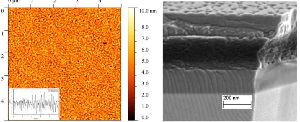
The surface quality of the substrate is crucial for epitaxial thin film fabrication. Thin films with smooth surfaces/interfaces are highly desirable for multilayer device fabrication. Similarly, the microstructure of the deposited film has important consequences on the ferro and piezoelectric properties of ferroelectric oxide thin films. Considering this, surface morphology and microstructural investigations of the substrates and deposited films were performed by atomic force microscope (AFM) and high resolution scanning electron microscope (HR-SEM).
Atomic force microscopy (AFM) is one of the scanning probe microscopy techniques that can be used to analyse the surface properties of the substrates and the thin films. AFM studies reported in this dissertation were performed on Bruker Icon. This instrument is capable to analyse topography, conductivity, ferroelectric properties, piezoelectric properties, elastic properties, thermal properties and magnetic properties. The images reported in this thesis were acquired by operating the instrument either in contact mode or tapping mode. In contact mode operations, the cantilever tip constantly remains in contact with the sample surface during scanning. This imaging mode is heavily influenced by frictional forces due to strong tip sample interactions. This can damage the sample surface or distort the image data spatially in case of soft samples. Vertical deflection of the cantilever during scanning provides the dynamic feedback signal necessary to image the feature height on the sample surface. In tapping mode operation, the cantilever is oscillated at or near its resonance frequency. In this mode, forces between cantilever tip and sample surface cause a change in the initial resonance behavior. A
phase image can also be created by simultaneously monitoring the phase shift between drive signal to the cantilever and its response. The AFM setup is schematically shown in figure 2.4.
Figure 2.4: Simplest schematic view of the Atomic Force Microscope
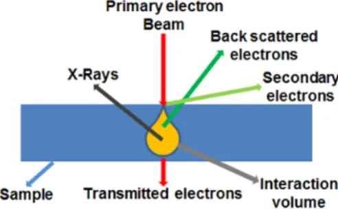
Scanning electron microscopes (SEM) fall in the category of electron microscopes because they employ electrons for imaging instead of light. The scanning electron microscope images reported in this dissertation were taken by Zeiss Merlin HR-SEM. This instrument can be operated with an acceleration voltage ranging from 20V to 30kV and have point resolution of 0.9nm in STEM (scanning tunnelling electron microscope) mode, or 1.2nm in normal SEM mode working with acceleration voltage of 30kV. This SEM is equipped with a number of detectors capable of measuring clear topography (SE & SE-2), compositional and crystal orientation mapping (ASB), compositional contrast (ESB), elemental analysis (EDX), conductivity mapping (EBIC) and crystal orientation mapping (EBSD). The simplest schematic view of the scanning electron microscope is shown in figure 2.5.
Figure 2.5: Schematic view of the scanning electron microscope
The electrons are emitted from the source (field emission gun in this case) and travel through the column that consists of anode, magnetic lenses and scanning coils placed in vacuum. This beam of electrons is used to scan the sample by scanning coils. Different kinds of interactions take place between the electron beam and the sample generating secondary electrons, back scattered electrons, characteristic x-rays etc. which are used to acquire the informations of interest. The interaction between primary electron beam and sample is schematically shown in figure 2.6.
Figure 2.6: Schematic view of the electron and material interaction used for
2.3.3 Electrical investigations
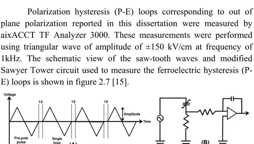
Polarization hysteresis (P-E) loops corresponding to out of plane polarization reported in this dissertation were measured by aixACCT TF Analyzer 3000. These measurements were performed using triangular wave of amplitude of ±150 kV/cm at frequency of 1kHz. The schematic view of the saw-tooth waves and modified Sawyer Tower circuit used to measure the ferroelectric hysteresis (P-E) loops is shown in figure 2.7 [15].
Figure 2.7: Schematic view of the saw-tooth wave used for hysteresis loop
measurements (A) and modified Sawyer Tower circuit (B).
The typical result of polarization verses electric field measurements is a hysteresis curve demonstrating the characteristics of the measured material. The commonly used nomenclature for the evaluation of the measured data is described with the help of typical hysteresis curve shown in figure 2.8.
Where
• Pr+: Positive remanent polarization • Pr-: Negative remanent polarization • Vc+: Positive coercive voltage • Vc-: Negative coercive voltage • Pmax-: Saturation polarization • Vmax-: Saturation voltage
• Pns: Non-switchable polarization • Psw: switchable polarization
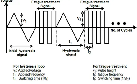
To investigate the ferroelectric response stability, polarization switching behavior (fatigue) tests were performed. Fatigue refers to the change of the hysteresis loop (P-E) with the number of switching cycles the ferroelectric capacitor has gone through. The ferroelectric capacitors were switched multiple times and the influence of the amplitude and frequency excitation signal on fatigue behavior was investigated as the number of switching cycles increases. The saw-tooth wave form excitation signals are usually employed to record the ferroelectric hysteresis loops whereas the rectangular excitation pulses are typically employed to achieve highest amount of instantaneous switching during fatigue treatments. The fatigue treatment process is schematically illustrated in figure 2.9. This method starts with the measurement of the initial ferroelectric hysteresis loop followed by fatigue treatment steps. The fatigue treatment process is interrupted in regular intervals to record the ferroelectric hysteresis loops in such a way that a logarithmic plot of data points can be acquired with an equal spacing. Typically result of the fatigue measurements is a plot between remanent polarization (extracted from P-E loops recorded in-between fatigue treatment) versus the logarithm of the total number of switching cycles.
Figure 2.9: Schematic view of the fatigue treatment process.
Epitaxial PMN-PT films are sandwiched between metallic electrodes (SrRuO3) to form a parallel plate ferroelectric capacitor. Capacitance of a parallel plate capacitor refers to charge stored in the ferroelectric capacitor. Capacitance verses electric field (C-E) measurements reported in this dissertation were performed using a Keithley 4200 semiconductor characterization system (Keithley Instruments GmbH, Germany). These measurements were performed in a frequency range of 10 kHz to 1 MHz by employing a small ac signal of 4kV/cm. The relation between capacitance and dielectric constant is given by.
Dielectric Constant: (2.1) The correlation between capacitance and dielectric losses (tanδ) is given by.
Dielectric loss: tan (2.2) Where
• ε : Permittivity of the material between the plates/electrodes (PMN-PT)
• C : Capacitance in Farads [F]
• εo : Dielectric constant of free space [8.854×10⁻¹² F/m] • A : Area of the capacitor in square meters [m2]
• G : Conductance in Siemens [S] • f : Frequency in Hertz [Hz]
The leakage current is another important characteristics which affects the performance of ferroelectric material based devices and need to be studied. The leakage current investigations (J-E) reported in this dissertation were performed using a Keithley 4200 semiconductor characterization system (Keithley Instruments GmbH, Germany).
2.3.4 Electromechanical investigations
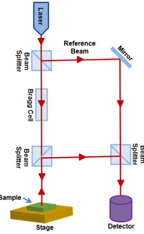
The piezoelectric properties of the epitaxial PMN-PT films and free standing cantilevers reported in this dissertation were measured with a Polytec MSA-400 Microsystem System Analyzer. This instrument is a combination of Scanning Laser Doppler Vibrometry, Stroboscopic Video Microscopy and White Light Interferometry. Laser Doppler Vibrometer (LDV) is a non-contact based instrument designed to measure out of plane vibrations [16-17]. The laser beam is directed towards the surface to be measured. Vibrations in the piezoelectric material induce changes in vibrational amplitude and frequency which can be detected through the Doppler shift of the laser beam. LDV is a Michelson interferometer based instrument that measures the difference in interference fringes which are caused by changes in length between the measured laser beam with respect to a reference laser beam [18]. This instrument can detect deformations with a resolution of roughly 5pm if good vibration filtering and a frequency higher than 500Hz are employed [19].
The laser doppler vibrometer utilizes a He-Ne laser operating at wavelength of 632.8nm. It is evident from figure 2.10 that the laser beam from the source is divided into two beams, one for measurement and other for reference. The measurement beam, after reflecting from
the vibrating sample, reaches the detector where it is combines with the reference beam to generate interference fringes. From the interference pattern, vibration frequency and amplitude can be deduced.
The longitudinal piezoelectric coefficients (d33) were derived from piezoelectric hysteresis loops which were measured by connecting additional electronics with the LDV [20]. These measurements were performed by employing dc signal of amplitude ±12 V at 8kHz frequency superimposed with a small ac-signal of 0.5 V. Basic Laser Doppler Vibrometer (LDV) setup is shown in the figure 2.10.
2.4 References
[1] T. H. Maimon, Nature, 187 (1960) 493.
[2] F. Breech and L. Cross, Appl. Spectrosc. 16 (1962) 59. [3] H. M. Smith and A. F. Turner, Appl. Opt. 4 (1965) 147.
[4] H. Schwarz and H. A. Tourtellotte. J. Vac. Sci Technol. 6 (1968) 373.
[5] A. Inam, M. S. Hegde, X. D. Wu, T. Venkatesan, P. England, P. F. Miceli, E.W. Chase, C. C. Chang, J. M. Tarascon, J. B. Wachtman, Appl. Phys. Lett., 53, (1988) 908.
[6] Robert Eason, Pulsed laser deposition of thin films: applications led growth of functional materials, John Wiley and Sons, Inc. New Jersey (2007).
[7] G. Rijnders, G. Koster, D. H. A. Blank and H. Rogalla, Appl.
Phys. Lett., 70 (1997) 1888.
[8] G. Koster, G. Rijnders, D. H. A. Blank and H. Rogalla, Appl.
Phys. Lett., 74 (1999) 3729.
[9] F. Fahler and H. U. Krebs, Appl. Surf. Sci., 61 (1996) 96-98. [10] Mark Huijben, Interface Engineering for oxide electronics,
PhD Thesis, University of Twente, 2006. (ISBN: 90-365-2351-6)
[11] S. E. Park, T. R. Shrout, IEEE Trans. Ultrason. Ferroelectrictr. Freq. Control. 44, (1997) 1140.
[12] M. Ohring, Material science of thin films. Academic press, London, 2nd Edition, 2002.
[13] S. Horita, T. Naruse, M. Watanabe, A. Masuda, T. Kawada, Y. Abe, Appl. Surf. Sci., 117–118 (1997) 429.
[14] P. Maitri, Warusawithana, C. R. Sleasman, J. C. Woicik, Y. Li, L. F. Kourkoutis, J. A. Klug, H. Li, P. Ryan, L. P. Wang, M. Bedzyk, D. A. Muller, L. Q. Chen, J. Levy, D. G. Schlom,
Science, 324 (2009) 367.
[15] Y. T. Tsui, P. D. Hinderaker and F. J. Mcfadden, , Rev. Sci. Instrum. 39 (1968) 1423.
[17] A. L. Kholkin, Ch. Wutchrich, D. V. Taylor, and N. Setter, Rev. Sci. Instrum. 67 (1996) 1935.
[18] Z. Haung, G. Leighton, R. Wright, F. Duval, H. C. Chung, P. Kirby and R. W. Whatmore, Sens. Act. A., 135 (2007) 660. [19] A. L. kholkin, C. Wutchrich, D. V. Taylor and N. Setter, Rev.
Sci. Instrum., 67 (1996) 1935.
[20] Minh Duc Nguyen, Ferroelectric and piezoelectric properties of epitaxial PZT films and devices on silicon, PhD Thesis, University of Twente, 2010. (ISBN: 978-90-365-3047-7)
3.
Processing of PMN-PT films
Chapter Overview:
This chapter describes the growth of perovskite phase and (001) orientation pure epitaxial PMN-PT thin films on SrRuO3 electroded SrTiO3 substrates.
The effect of fabrication conditions like laser energy density (fluency), substrate temperature, target to substrate distance and deposition pressure on phase formation was investigated in detail. Within relatively narrow processing window to achieve phase and orientation pure films, the effect of growth conditions on ferroelectric and piezoelectric properties of these films was studied.
3.1 Introduction
Micro-electromechanical systems (MEMS) based on ferroelectric oxides are among the highest performing devices for the purpose of sensing and actuation. Lead zirconium titanate (PbZr 1-xTixO3 or PZT) is one of the frequently employed piezoelectric materials for the fabrication of such devices [1-2].
An alternate to PZT are relaxor ferroelectrics like (PMN-PT), (PZN-PT) etc. which are solid solutions between a relaxor (PMN or PZN) and a ferroelectric material (PT). Recent developments in relaxor ferroelectrics yielding giant piezoelectric response compared to the well-known piezoelectric material PZT have propelled them to the forefront for sensors and actuators research and development. Park and Shrout reported ultrahigh strain in [Pb(Mg1/3Nb2/3)O3]67 -(PbTiO3)33 and [Pb(Zn1/3Nb2/3)O3]91-(PbTiO3)09 bulk single crystals oriented and poled in the (001) direction. Specifically PMN-PT (67/33) shows a record high piezo-electric coefficient ≈ 2500 pm/V [3]. In addition these materials exhibit significantly higher coupling coefficients (k33 ≈ 0.9) than bulk PZT ceramics. Due to their superior properties, devices fabricated from these materials may generate large strains for small applied field or vice versa be sensitive to very small strain [3-4].
PMN-PT is a crystalline solid solution of a typical relaxor (PMN) and a classic ferroelectric material (PT). In many ferroelectric solid solutions, the dielectric and piezoelectric properties are maximized at the morphotropic phase boundary. This morphotropic phase boundary occurs at 33 percent of PT in the bulk PMN-PT solid solution system. Nevertheless thin film boundary conditions like clamping to the substrate can modify the morphotropic phase boundary. This behavior is not entirely clear for epitaxial PMN-PT thin films. Giant piezo response up to 1.7% , an order of magnitude higher than for bulk PZT ceramics, was observed for (001) oriented PMN-PT (67/33) single crystal. This ultra-high strain in PMN-PT
single crystals is attributed to electric field induced phase transformations from the rhombohedral to the tetragonal phase. Furthermore, the high coupling coefficient (k33 > 0.9) and low dielectric losses (<1%) make this material a promising candidate for the fabrication of new generation sensors and actuators [3].
For many applications, one requires PMN-PT in thin film form instead of bulk single crystals. This necessity initiated efforts to synthesize this hyperactive material in thin film form. Epitaxial films are highly desirable compared to polycrystalline films due to a lower leakage current and higher piezo response [5-6]. The growth of high quality epitaxial PMN-PT films is known to be difficult because of the relatively poor thermodynamic stability of the perovskite phase and compositional complexity. The prominent, stable pyrochlore phases like cubic Pb3Nb4O13, rhombohedral Pb2Nb2O2 and tetragonal Pb3Nb2O8 appear during growth. These non-piezoelectric phases cause degradation of the functional properties of the deposited films [7-8]. Additionally, the properties of PMN-PT films are sensitive to film stoichiometry and all five elements should be in exact stoichiometry to achieve good properties. Off stoichiometry not only degrades the film properties but also can cause the formation of impurity phases (pyrochlore phases). For instance, epitaxial films are usually deposited at high substrate temperature which may result into lead loss due to its high volatility. Lead loss not only promotes higher leakage current but also can cause the formation of lead deficient pyrochlore phases. It is noticed that PMN-PT is commonly preferred over PZN-PT, since the later contains two volatile elements (Zn and Pb) although both exhibit superior properties compared to the prominent (PZT) ferroelectric material. Besides the lead stoichiometry, the Mg/Nb ratio is also found essential to fabricate perovskite phase pure PMN-PT films [9].
A number of methods and approaches has been adopted to fabricate high quality PMN-PT material. For instance, the columbite process was developed by S. L. Swartz and T. R. Shrout in 1982 for the synthesis of bulk PMN-PT ceramics. This process bypasses the pyrochlore phase formation by facilitating the reaction between MgO
and NbO prior to the addition of and reaction with PbO [10]. Nonetheless, this method is not useful for thin film growth. Maria and co-workers were the first who successfully deposited epitaxial PMN-PT (70/30) thin films, using pulsed laser deposition (PLD) on LaAlO3 substrates. They achieved perovskite phase pure epitaxial PMN-PT(70/30) films by carefully controlling the fabrication conditions. [11]. Subsequently S. D. Bu et al. adopted the approach of miscut SrTiO3 (STO) substrates to achieve perovskite phase pure epitaxial PMN-PT(67/33) films. The high density of steps on the miscut substrate surface was thought to promote the growth of the perovskite phase by facilitating the incorporation of volatile PbO into the film. [12]. Afterward S. H. Baek et al. demonstrated the fabrication of high quality epitaxial PMN-PT(67/33) films with giant piezo response on SrTiO3 buffered miscut silicon substrates [20]. High quality epitaxial PMN-PT films have been deposited using metal-organic chemical vapor deposition, sputtering and pulsed laser deposition [11-14].
From the literature, it is clear that the deposition of high quality PMN-PT films is very sensitive to the deposition conditions and only a very narrow process window exists. Further within this window the piezo and ferroelectric properties of the films are varying strongly with the exact process conditions. It is therefore important to establish the process window (which is clearly somewhat specific for the deposition equipment used) and the (qualitative) relation with the properties.
In the first section of this chapter we describe the optimization of the growth of epitaxial PMN-PT thin films on STO substrates by varying the deposition conditions and find a very narrow process window for phase-pure growth. In the second part the variation of the ferroelectric properties within this process window is investigated.
3.2 Experimental Procedure
3.2.1 Samples fabrication
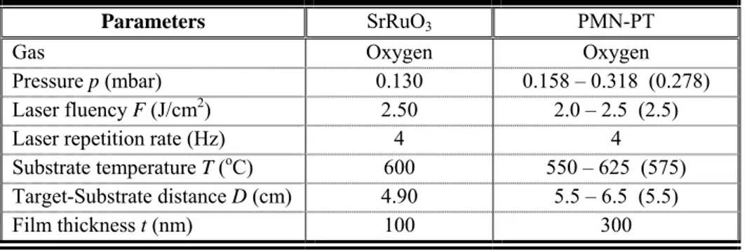
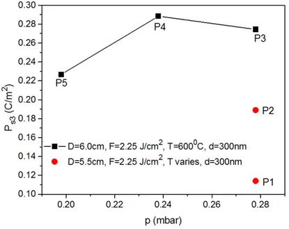
For this study (001) oriented STO substrates with B-site termination were used for their well-defined crystalline surface and close lattice match to the thin films. The STO substrates were pre-treated to achieve B-site termination using method developed by Koster and co-workers [24]. 100nm thick SrRuO3 (SRO) thin films were deposited as top and bottom electrodes, because SRO can grow uniformly on a TiO2 terminated STO substrate with a high crystalline quality [17]. Secondly the use of oxide electrodes is very beneficial for the long-term stability of ferroelectric oxides, as compared to metal electrodes [18,19]. For the ferroelectric the PMN-PT(67/33) composition was selected because of its giant piezoelectricity in thin film form on STO-buffered silicon demonstrated in ref.[20]. All films have been deposited with Pulsed Laser Deposition (PLD) using a KrF Excimer laser operating at 248nm, using commercial targets on a heated substrate. The deposition conditions are given in table 3.1.
Table 3.1: Growth conditions of SRO electrodes and PMN-PT films on STO(001)
substrate. (In brackets the initial conditions used prior to the optimization)
Parameters SrRuO3 PMN-PT
Gas Oxygen Oxygen
Pressure p (mbar) 0.130 0.158 – 0.318 (0.278) Laser fluency F (J/cm2) 2.50 2.0 – 2.5 (2.5) Laser repetition rate (Hz) 4 4 Substrate temperature T (oC) 600 550 – 625 (575)
Target-Substrate distance D (cm) 4.90 5.5 – 6.5 (5.5) Film thickness t (nm) 100 300
The complete SRO/PMN-PT/SRO heterostructure was deposited without breaking the vacuum. After deposition the samples were cooled down to room temperature in a pure, 1 bar oxygen