F
ACOLTÀDII
NGEGNERIALAUREA SPECIALISTICA IN INGEGNERIA ELETTRONICA
“Development of a control system for superconducting cavities
with fast tuners”
RELATORI
IL CANDIDATO
_________________________
___________________
Dott. Ing. Giovanni Pennelli
Matteo Scorrano
Dipartimento di Ingegneria dell'informazione
_________________________
Dott. Franco Bedeschi
INFN PISA
Acknowledgments
Prima di tutto un grazie di cuore alla mia famiglia, che mi ha sostenuto nel
periodo dei miei studi.
Successivamente ringrazio tutti coloro con cui ho condiviso l'esperienza
universitaria: Andrea (e le passeggiate serali verso mensa Cisanello), Pierpaolo,
Carolina, Nuri, il tubo di “Pitot” che tanto mi è rimasto impresso ascoltando i
discorsi tra aerospaziali(senza dimenticare il diffusore della McLaren), Sandro
con cui ho “sofferto” nelle varie biblioteche nel rush finale per il mio ultimo
esame e del suo “Costruzioni di macchine”(se non ricordo male...), Daniele (il
bummone) che ormai si è evoluto ed è immerso nei 7 e 30 delle vecchiette di
Zanni, Maurizio, Claudia, Nicola, tutti i ragazzi della GMV Basket Ghezzano,
Angela, Alessandro, i suoi mille soprannomi (smile, manduccio, jp, fred mello,
coccia quadrata, ecc.) e Massimo.
Ringrazio inoltre tutte le persone con cui ho condiviso l'esperienza americana,
soprattutto (Translation : “I thank all the people with whom I shared the american
experience”) : Emanuele, Antonio, Alessandro, Giuseppe, Roman, Dilip, Ali
(Thanks for the “word of the day”).
A special thanks to Warren Schappert for everything he taught me.
I want to thank Franco Bedeschi, Yuriy Pischalnikov and Ruben Carcagno for the
great opportunity I was given.
Grazie a tutti voi! (Thank you all!)
Abstract
The purpose of this thesis is to develop a control system for superconducting
cavities, which are the key elements of linear accelerators. In this case the
cavities are resonant filters fed with an electromagnetic field at 1.3 GHz. The
system works on the compensation of mechanical distortions with fast tuners.
Mechanical distortions modify the resonance frequency of the cavities causing
significant inefficiency in the acceleration process. Typical high energy linear
accelerators consist of thousands of cavities so a compensation system is
required in order to avoid huge power losses.
The first part of the thesis is the work I have done to understand the detuning
sources, and the kind of controls needed for each source (described in chapter
1). The second part is a survey of electronic boards that can achieve the goal
with the lowest cost and high flexibility (chapter 2). The next step of my work
consists of the study of the processing needed for each kind of detuning sources
(chapter 3), making it easy to develop, to modify, to test and to improve using
LabView FPGA and MATHSCRIPT on an existing National Instrument system.
Another important enhancement that is achieved is to speed up the transfer of
data to the FPGA through the FIFO block of LabView by modifying the codes
written for hardware implementations using VHDL, C++, and LabView
programming
Table of contents
Abstract
Table of contents
1.
Introduction
1.1 Overview
1.2 Description of Piezo stack actuator
1.3 Sources of detuning
2.
Old system and new solutions
2.1 Old system description
2.1.1 Description of the control system(LF and pressure compensation) 2.1.2 Description of the control system(Microphonic distortions)
2.2 Description of thesis targets
2.2.1 Cost analysis 2.2.2 SbRIO description
2.2.3 Via processor + Nexys2 description
3.
Processing
3.1 LF and Pressure compensation general description
3.2 Microphonics compensation description
3.2.1 FIR filters 3.2.2 IIR filters
4.
Software description
4.1 General description
4.1.1 Host part description 4.1.2 FPGA part description
4.
4.2 PXI preliminary test
5.
4.3 Transport of the on cheaper boards
4.3.1 SbRIO
4.3.2 Fanless board + Nexys2
4.4 Comparison
5. Tests
6. Appendix A
Chapter 1 – Introduction
1.1 - Overview
This work is a small part of ILC project (International Linear Collider), a new kind
of linear particle accelerator. The accelerators are machines used to accelerate a
particles beam in order to study the results of the collisions to discover the nature
of the matter. There are many ways to accelerate particles, but RF cavities are
one of the most common. The elementary parts of the ILC accelerator are the
TESLA cavities.
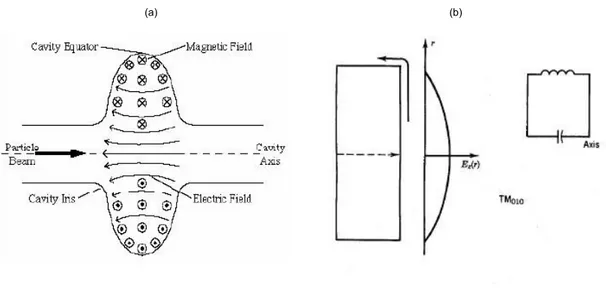
Figure 1.1: An example of TESLA cavity
The Tesla cavities are about 1 meter long and they consist of 9 cells of niobium;
this material has superconducting properties that significantly reduce power
consumption due to joule thermal dissipation. The superconducting effect needs
a very low temperature; therefore the system is cooled by being submerged in
Helium bath at 1.8 K during operation.
The system can work either with RF pulse or in continuous wave. This work is
done for pulsing operations. The typical field distribution in a cell is TM
0n0 .(a) (b)
Figure 1.2: Field distribution in a cell(a). Electrical field and equivalent circuit of a cylindrical cavity
The electrical field is maximum in the cavity longitudinal axis. The particle beam
have to be synchronous with the RF pulse in order to be continuously
accelerated. The spacing between the cells, the RF frequency, and the relative
phase of each cavity is chosen to get the maximum acceleration. These cavities
are excited by a sequence of RF pulses at 1.3 GHz spaced 0.1 seconds; during
each pulse a stream of particle bunches can be accelerated. This frequency is
optimal for the acceleration efficiency of these cavities. The electrical behavior of
the cavities is like a resonance filter at 1.3 GHz of central frequency with a very
high quality factor (Q =
3
×
10
6) which allows to have a very narrow band around
the central frequency (about 200 Hz). If for any reason the cavity gets deformed,
the central frequency of the filter changes and the system efficiency decays. It is
possible to create a very strong electrical field by exciting the electrical
resonance with an oscillating voltage. It means that an electron or proton coming
in one end of the cavity leaves the other end with 35 MeV more kinetic energy
than it came in with (if the cavity is filled of a field at 35 MV/m). An ever larger
collision energy
is needed from the collision
, in order to discover new kind of
particles. Therefore it is very important to compensate any source of energy
wasting in order to cut cost and improve acceleration efficiency.
Figure 1.3: Cryomodule
The cavities are arranged in groups of eight and they are put inside the
Cryomodules. At the end of the ILC project several Cryomodules will be placed in
cascade to sum the contributions of each individual cavity. Two very long “arms”
(10 Km) will be placed in front of each other in order to have a high collision
energy with a total center of mass energy between 500 and 100 GeV.
Each cavity has two kinds of tuning systems: the first one is a slow tuner and the
second one is a fast tuner. The slow tuner uses a stepper motor to set static
operating frequency; this essentially compensates for the change of cavity
dimensions due to the cooling process from room to cryogenic temperature. The
fast tuner uses piezo actuators to compensate the time dependent detuning. The
control system must determine the detuning of the cavity, calculate the optimum
waveform for the compensation and drives the piezo actuator to keep cavity in
tune during RF pulse.
The main purpose of this thesis is to develop a control system for the detuning
caused by Lorentz force on the cavity walls and pressure fluctuations. A second
purpose is to develop a control system for the microphonic noise compensation.
After compensation the residual detuning of the cavities should be 20 Hz or less
at an accelerating gradient of 35 MV/m.
1.2 - Description of the Piezostack Actuator
The most important actuator for the system is the piezo stack located on the
cavities.
This kind of piezo actuators are commercially available and they are usually used
at room temperatures (RT) but we need to work at cryogenic temperature (CT)
so these actuators are used with a reduced stroke than at RT (6-10% of RT
stroke).
The keys features of those piezo actuators are:
1) Resolution:
1001
nm
However the resolution is limited by the noise characteristic of the power supply.
2) Polarity: the polarity in general is only positive (0 to 150 V), but a very little
negative polarity is allowed (<10% of the maximum voltage).
3) Resonant frequency: typically 5-50 KHz
The piezo actuators usually are oscillating mechanical systems. The value which
characterizes the dynamic behavior of the piezo is the resonant frequency. The
resonant frequency depends by the stiffness and mass distribution within the
actuator.
The rise time depends on the resonant frequency, so this parameter is very
important for the description of the dynamic behavior of the piezo.
4) Capacitance: a piezostack actuator consists of thin ceramic plates as dielectric
and electrodes. This is a system of parallel capacitors. Typical capacitance
values are 60 nF for the high voltage actuators.
Figure 1.5: An example of piezostack structure.
The very high resolution of the piezoelectric actuators allows the use of these
devices on the nm-positioning field. That is why they can be used in this project.
However, there are some problems with the hysteresis which makes the voltage
and motion relation not unique.
This is something to consider whether a high resolution or repeatability are
necessary for the application.
Another important source of disturb is the noise on the power supply. A voltage
fluctuation of the power supply ∆U means a mechanical movement ∆x. That is
why usually a low noise power supply is used for this kind of applications.
The typical inner resistance is about
10 Ω, so there are no high current
10problems in static or semi-static applications but they may occur in high
frequency applications due to the piezoelectric capacity. It is an important factor
to consider for the piezoactuators reliability.
1.3 - Description of the sources of detuning
There are three principal sources of mechanical distortions:
1) Lorentz force detuning
2) Microphonics
3) Pressure Fluctuations due to the helium bath
The Lorentz force detuning is due to the RF pulse used to feeds the resonant
filter: the electromagnetic field inside the cavity interacts with the induced
currents on the cavity wall causing a shape distortion (shrink, stretch, bend of the
filter body). These deformations bring the system out of the resonance zone and
then the accelerating efficiency drops.
It is possible to increase the cavity wall thickness to improve the rigidity but it
causes less cooling efficiency and then a bigger power consumption than a
thinner wall cavity. It is necessary to find a compromise for this trade off.
The detuning strongly depends on the electrical field gradient. LF can detunes
the cavity up to 400 HZ, a twice of the cavity bandwidth, with an accelerating
gradient of 25 MV/m.
The LF detuning effect is the same from pulse to pulse and then it is a
deterministic phenomenon so the compensation can be accomplished by a
feed-forward control system .
The microphonics sources are the external vibrations (car traffic, seismic noise
and other vibration sources). It requires a fast feedback loop because the
microphonics noise have a typical mechanical bandwidth of 1 Khz.
The pressure fluctuations are due to the pressure changes in the vessel where
the cavities are cooled down. Those fluctuations are very slow (bandwidth << 1
Hz). This kind of disturb is compensated with a slow feedback loop.
The last two kinds of disturbances are stochastic, so the processing is different
than the processing for the Lorentz force detuning.
Chapter 2 – Old system and new solutions
2.1 - Old System description
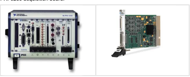
The old system has been developed on a PXI-1042, National Instruments crate
equipped with PXI-7833R (FPGA 3M gates Virtex II (40MHz),analog I/0 16 bit
resolution sampling rate up to 200 KHz, output update rates up to 1 MHz and 96
digital lines), PXI-8105 (2.0 GHz Intel Core Duo T2500 dual-core processor) and
PXI-6289 acquisition board.
Figure 2.1: An example of PXI-1042 crate and plug-in module
This solution uses a course version of a LabView program. This program is
composed of a CPU part and a FPGA part. The CPU part gets the data
manually and load them on the FPGA memory. It basically uses the LabView
FPGA interfaces for the CPU/FPGA communication. The FPGA part uses
LabView HDL node, which have a core of low level VHDL code. The VHDL code
implements two principal components: a FIR filter used for the microphonics
compensation (It was not working) and a playback block which repeats the
Lorentz force detuning waveform each trigger pulse.
It is possible to add an offset to the output signal to compensate the time
independent component of the distortion.
This system has been repaired and completed because of urgent need of tests
on the real cavity.
2.1.1 - Description of the control system (LF and Pressure
compensation)
The control system drives a power amplifier and stepper motors. The amplifier
drives the piezo stacks of the fast tuner. Those components are used to
compensate the shape distortion of the cavity.
The stepper motor is currently set before to start the activity on the cavities; it is
switched off during the operations.
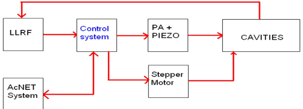
The following figure shows the block diagram of the whole system.
Figure 2.2: Block Diagram of the whole system (In blue there’s the control system developed in this thesis)
The Control system has a principal input from the LLRF system (Low Level RF).
The LLRF system acquires all the data from the cavity and converts the analog
RF signal to a digital information. The signal contains data about cavity states
and control information. Another important I/O to consider for future
developments is the AcNet Network.
The AcNet is a network used at Fermilab to create the possibility of monitoring
and synchronization of all the electronic systems through a common
communication standard.
In this thesis I work only on the fast tuners so the only one output is the power
amplifier and then the piezoactuators.
The system calculates the optimum waveform for the detuning compensation and
drives the power amplifier.
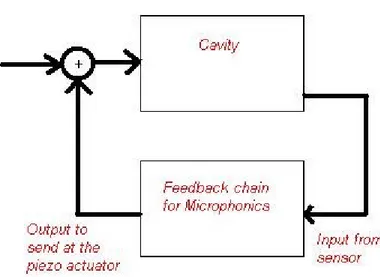
2.1.2 - Description of the control system (Microphonics distortions)
The microphonics control system works in feedback loop because microphonics
is a stochastic process. The reaction chain input can be contained in the LLRF
digital signal or can be acquired directly from a sensor situated in the cavity, then
the system must be able to handle digital and analog input. The signal is from an
accelerometer situated in the cavity or from a piezostack used as sensor. The
output is sent to the power amplifier (the signal is summed to the LF waveform
and the offset).
The optimum waveform processing algorithm is still in development. The idea is
to create an adaptive filter which gives the opposite phase and the same
amplitude of the input signal in order to erase all the frequency peak of the
mechanical vibrations.
2.2 - Description of the thesis's targets
The existing system is too expensive; it costs around 10K$ per cryomodule and
the accelerator will have thousands of cavities so the cost will be too high.
Therefore the main target is the feasibility study on cheaper boards.
The system requirements are:
1) The system must communicate through the AcNet network
2) The system must receive a digital signal (maximum bit rate 1.15 Mbit/s)
from the LLRF crate
3) The system must have at least one CPU for the waveform processing and
for communication and driving management.
4) The system must be equipped of enough outputs to drive a whole
cryomodule.
2.2.1 - Cost Analysis
A low system price is required for an industrial distribution. Nowadays the price is
too high. The next step is to find a good trade off between the costs and the work
complexity. The last step, later than this thesis, will be to get the lowest price
board for manufacturing.
The design method has to be focused on re-usability, in order to make easy
each step.
Figure 16: The costs road predicted.
The work done in this part is to make a spreadsheet about all the characteristics
and costs of the possible solutions.
The most interesting solutions are:
-Single Board RIO (SbRIO) of National Instruments. It is easy to develop
because the old code is from a NI board.
-The processor VIA Eden on a fanless motherboard and the FPGA board
Nexys2. This is the cheapest solution and it is possible to keep the CPU part of
the old Labview code. The FPGA is programmed through low level VHDL.
Both these solutions can satisfy the entire requirements.
The other solutions have problems like a big development time, license too
expensive or interface problems.
The old Labview license can be used for this project and it is a good start to cut
the costs.
2.2.2 - SbRIO Description
Figure 2.4: Picture of sbRIO
The single board RIO is a prototyping
board of the National Instruments. It has
a Freescale real-time processor at a
frequency of 400MHz and a 2M gate
Xilinx Spartan-3 FPGA (40 MHz main
clock). Moreover it has up to 128 MB
DRAM and 256 MB of nonvolatile
storage, RS232 ports very useful for
expansions with plug-in boards,
Ethernet port useful for the
.
communications with the other systems. It is completely programmable through
LabView. It is not possible to get only one piece of any kind of SbRIO . Therefore
NI provides an evaluation board (RIO-EVAL-101) with a little daughter board
(EVAL-RIO-02) which provides I/O ports.
The I/O characteristics are:
Analog Input (sbRIO-961x/963x/964x only)
Number of channels... 32 single-ended or 16 differential
ADC resolution... 16 bits
Conversion time ... 4 μs (250 kS/s aggregate)
Nominal input ranges ... ±10, ±5, ±1, and ±0.2 V
Analog Output (sbRIO-963x/964x only)
Number of channels... 4
DAC resolution... 16 bits
Update time (one channel) ... 3 μs
Output range ... ±10 V2.2.3 - Via processor + Nexys 2 Description
Figure 2.5: Fanless board VIA Eden
The fanless board is equipped with a
VIA Eden CPU 1.2 GHz, and the power
consumption is only 7W. It is also
equipped with two Ethernet plugs, six
USB connectors and the plugs for
mouse, monitor and keyboard. The
operative system is Windows XP so it is
possible to run a Labview executable file
on this cpu.
Figure 2.6: Nexys2 FPGA.
The NEXYS2 works at a frequency of
50 MHZ and it has a Xilinx Spartan-3
1200K gate on board. Moreover it has
USB connectors useful for the
communication with the fanless board
and the PMOD connectors used to add
daughter boards for the D/A and A/D
conversion.
PMOD
Figure 2.7: PMOD, plug in of Nexys2 board.
The PMODs are inserted on the Nexys2
board into the connectors. They increase
the features of the FPGA system.
We use DAC and ADC; the resolution of
both the converter is 12 bits. They are a
good start to try the device.
Chapter 3 - Processing
3.1 - Lorentz force & Pressure compensation general description
The LF and pressure compensation processing is divided in two main parts. The
first one is the Steady State Operation and the second one the Startup
Procedure.
Steady State Operation
During operation the major task of the CPU is monitoring the detuning of the
cavity and control the piezo bias voltage to compensate for liquid helium
pressure fluctuations.
The detuning of the cavity can be determined by transforming the envelopes of
the forward and probe signals into the frequency domain and using a least
squares fit to determine the step for the interpolation (the forward signal is the RF
signal which is sent to the cavity, the probe signal is the output of the cavity).
During tests on the cavity a running exponentially weighted average of the
detuning is used to track resonance frequency changes and set the piezo bias
voltage.
Startup Procedure
When the cavity is first turned on or when cavity operating conditions change (for
example the accelerating gradient) a procedure to determine the appropriate LF
compensation waveform is performed. As the first step of the startup procedure,
the DC bias on the piezo is set to half the full range of the actuator. The slow
stepper motor tuner is then used to bring the static cavity resonance frequency
close to the target operating frequency.
This part is a course frequency scan. It is performed manually but in future we
want to use AcNet communication to perform this work. The stepper motor is
turned off after this operation in order to avoid a warming up of the cavity which
can compromise the behavior of the system.
Once the slow tuner has brought the cavity close to resonance, the piezo DC
bias is set to zero and some number (typically 10) RF pulses are recorded. The
important thing is to have enough pulses to make the average and reduce the
noise. The number of pulses is arbitrary. The bias is then increased by 10 volts
and another set of pulses is recorded.
This procedure is repeated until the full scale voltage of the piezo (100 V or 150
V) has been reached.
The RF pulse sent to the cavity (Forward signal) and the output signal (Probe
signal) are measured. The function Probe/Forward versus phase is plotted.
-2 0 - 1 0 0 1 0 2 0 3 0 4 0 5 0 6 0 7 0 1 . 1 5 1 . 2 1 . 2 5 1 . 3 1 . 3 5 1 . 4 1 . 4 5 1 . 5 x 1 01 7 p i e z o s c a n _ 2 0 0 9 0 1 2 1 1 5 5 2 . m a t P h a s e O ffs e t : 3 1 . 8 8 D e g r e e s P h a s e ( D e g r e e s ) P ro b e /F o rw a rd
Once the plotting operation is finished the phase at the peak has to be found.
Now the piezo voltage versus phase is plotted and the value at the optimum
phase may be found.
An interesting and important parameter to calculate is the detuning. It is an index
of how far the system is from the resonance. The best formula which achieve this
target is the following:
dP /dt=−
half
i∗ P2∗
half∗
F
Where P and F are the complex signals Probe and Forward, delta is the detuning
and omega half is the half bandwidth around the resonance frequency.
- 1 0 0 - 8 0 - 6 0 - 4 0 - 2 0 0 2 0 4 0 6 0 8 0 1 0 0 - 2 0 0 2 0 4 0 6 0 8 0 1 0 0 1 2 0 p i e z o s c a n _ 2 0 0 9 0 1 2 1 1 5 5 2 . m a t P i e z o B i a s V o l t a g e 4 9 . 4 V D C P h a s e ( D e g r e e s ) P ie z o V o lt a g e
Figure 3.2: Piezo Voltage versus phase
The piezo voltage at the optimum phase can be found through this graph.
Once the cavity resonance has been set the cavity is excited by a sequence of
short (2ms), small amplitude (10 V) piezo pulses. One piezo pulse is sent for
each RF pulse. The timing of the piezo pulses respect to the RF pulse is
systematically varied between 10ms before to 10 ms after the RF pulse in 1 ms
increments.
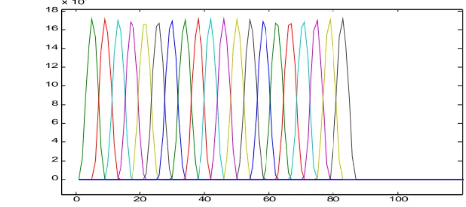
0 5 0 1 0 0 1 5 0 2 0 0 2 5 0 3 0 0 0 0 . 5 1 1 . 5 2 2 . 5 3 3 . 5x 1 0 4Figure 3.3: RF Forward signal
This is the forward signal. It is
sent to the cavity's antenna. It’s
formed by two principal parts:
the fill zone and the flap top
zone.
The first one is used to fill the
cavity of field. The second one
is used to accelerate the
particles beam. The rest is
noise. The total duration of the
pulse is 800 microseconds.
0 5 0 1 0 0 1 5 0 2 0 0 2 5 0 3 0 0 0 0 . 5 1 1 . 5 2 2 . 5x 1 0 4Figure 3.4: Probe signal at the output of cavity.
The information about the detuning is in the phase difference between forward
and probe signal. The phase is the most sensitive way to measure the detuning
of the cavity.
0 5 0 1 0 0 1 5 0 2 0 0 2 5 0 3 0 0 - 1 5 0 - 1 0 0 - 5 0 0 5 0 1 0 0
Figure 3.5: An example of phase difference between forward signal and probe signal
The data collected in this way are used to construct a response matrix of the
phase to piezo impulses of different delays. This matrix can be inverted and the
inverted matrix can be used to calculate the piezo waveform that will best keep
the cavity on resonance during the RF flattop. Once the piezo waveform has
been determined, it is uploaded into a memory. The processing in the
development system consists primarily of matrix operations and Fourier
transforms.
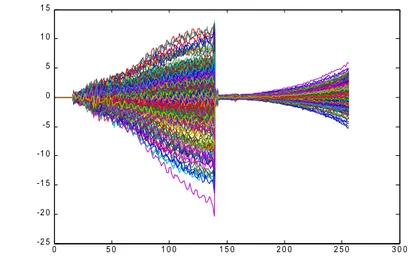
0 20 40 60 80 100 0 2 4 6 8 10 12 14 16 18x 10 7Figure 3.6: A plot of the pulses, one for each delay. The RF pulse arrives in the middle, about 40. It’s just a qualitative graph
5 1 0 1 5 2 0 1 0 2 0 3 0 4 0 5 0 6 0 7 0 8 0 9 0 1 0 0 0 2 4 6 8 1 0 1 2 1 4 1 6 x 1 07
Figure 3.7: The colors are the magnitude, X-axis number of pulse, Y-axis delay.
The next operation is to subtract the mean difference phase to the difference
phase between forward and probe signal.
0 5 0 1 0 0 1 5 0 2 0 0 2 5 0 3 0 0 -2 5 -2 0 -1 5 -1 0 -5 0 5 1 0 1 5
Some delays have positive phase other delays have negative phase. If the piezo
pulse comes before the RF pulse, it can change the phase positive or negative
depending on the delay. If it comes after the RF pulse, it has no effect. Because
each piezo pulse implies cavity vibration, and the measurements are done during
the RF pulse. Therefore the effects of vibrations are not present if the piezo pulse
arrives after the RF pulse. That is why for the delays which the piezo pulse
arrives after the RF pulse there are not big variations, only the vibration due to
noise.
The following graph (Figure 3.9) shows a plot of the phase between forward and
probe signal versus the delay of the piezo pulse. In this graph is possible to see
that when the piezo pulse is after the RF pulse the phase is almost constant.
0 5 0 1 0 0 1 5 0 2 0 0 2 5 0 3 0 0 - 2 5 - 2 0 - 1 5 - 1 0 - 5 0
The data may be processed with Matlab and the code can be used on LabView
through Mathscript node.
The figure 3.10 shows the inputs (left) and outputs(right) of the HV amplifier for
each delay. The first row of graphs shows the signals of the real system. Some
RF pulses at the beginning and at the end and when the delay is changed have
no piezo waveform. In the real system one piezo pulse for each delay group is
stored in a memory and it is sent to the actuator ten times. In order to have a
more clear interpretation of the data, in the two graphs for the processing (the
second row of graphs) the single pulse sent to the memory is drawn ten times so
there’s a correspondence between each piezo pulse in input of HV amplifier and
the respective output. Furthermore where there are no piezo pulse for the RF
pulse (the first and the last row in the real system graphs), the draw has been
erased, so only the informative signals are collected for the processing.
At this point we need to find the optimum waveform to send to the piezo actuator.
For this purpose we have an array containing the phase response on the flattop
to the RF signal alone(variable
y ), another one containing the phase response
0on the flattop to the combined RF and piezo pulses(variable y) and the last one
containing the amplifier input waveform for each RF pulse(variable V
piezo).
The linearity of the phase response to the piezo pulses is assumed
( y= y
0∗
V
piezo).
Inverting this equation the alpha parameter may be determinate.
The linearity of the phase response to RF pulses is assumed.(
y
0=∗
V
forward).
If we send a piezo waveform
V
PiezoOptimal= -
α
−1*
β
*
V
forwardwe will get y = 0
(
α
−1*
0y =
V
PiezoOptimal).
- 1 0 0 1 0 2 0 3 0 4 0 5 0 6 0 7 0 8 0 9 0 - 2 . 5 - 2 - 1 . 5 - 1 - 0 . 5 0 0 . 5 1 1 . 5 2 x 1 09Figure 3.11: A qualitative example of
V
PiezoOptimal waveform.This waveform is stored in a memory and the signal is sent to the HV amplifier
each RF pulse.
3.2 - Microphonics compensation general description
The processing of the microphonics compensation is still in development as
mentioned in cap 2 paragraph 2.1.2. The key component of the system is a
digital filter which reverse the phase of the noise signal and send the output to
the piezo amplifier. Therefore the spectrum of the input signal has to be scanned
in order to find the peaks in the frequency domain. Once the frequency peaks are
detected, the CPU perform all the operations to calculate the filter taps.
The old filter was a FIR filter. Another solution could be an IIR filter. The
important for this thesis is to start to work on this problem. The best solution can
be found in future developments.
3.2.1 - FIR Filters
FIR stands for Finite Impulse Response. The FIR filter implements a convolution
between the taps and the input samples.
Figure 14: FIR Filter block diagram
The output signal formula is
(
)
(
)
0
∑
=−
⋅
=
N i ix
t
i
c
t
y
. The FIR filter needs a memory
with enough space for the coefficients and one memory used to hold the samples
of the input signal (it needs to charge a new sample each new cycle of sampling).
It’s a good solution because there are no closed loop so there are no problems of
stability.
3.2.2 - IIR FILTERS
IIR stands for Infinite Impulse Response. The block diagram of an IIR filter is:
Figure 15: IIR Filter block diagram
The output signal formula is
(
)
(
)
(
)
0
t
v
i
t
y
b
t
y
M i i⋅
−
+
−
=
∑
=. The difference respect a
FIR filter is that it works using a reaction closed loop so some problem with
instability may occur. The only one gain respect a FIR filter is that it needs a less
number of taps for the same filter order and than a smaller memory is required.
Chapter 4 - Software Description
4.1 – General Description
The LabView software consist of two main parts: the Host part and the FPGA
part. The Host works on the CPU, the other part works on the FPGA. Therefore a
CPU/FPGA interface is implemented.
4.1.1 - Host Part Description
The host part has three key components: two for the LF waveform and filter taps
processing and one for the FPGA memory samples loading.
The first part developed in this thesis is the memory driver.
Figure 4.2: Data sender Labview code.
This program reads data from a file and sends them to the FIFO. The FIFO is a
first in first out memory stack located on FPGA and CPU memory. The FIFO has
been configured as DMA and Host to Target communication; it means the CPU
can perform the processing during the memory driving process and that we are
interested to send data from the CPU to the FPGA. Dimension and data format
can be configured inside the FIFO properties menu.
Figure 4.3: An example of FIFO Properties.
In order to use the FIFO in DMA configuration the Invoke Method has to be used
in the host VI.
Figure 4.4: Invoke method block
This block can be used to read and write the FIFO using the DMA so it doesn’t
take CPU time. In this case the read function is not allowed because the FIFO is
set as Host to Target so just the write function can be used. This Block needs a
FPGA VI reference, it is a pointer to the FPGA VI inside the real FPGA and it can
read more than one element per time (4096 elements because the filter length is
4k).
The fully configured block is shown in figure 4.2 inside the first part of the flat
sequence.
Another important block of this host VI is the read/write control function.
Figure 4.5: Read/Write control function block
This block allows to read and write into controls and indicators of the FPGA VI. It
needs just the FPGA VI reference and all the controls and indicators will appear
below the pink part of the block (as you can see in figure 4.2).
The rest of the code is used for the synchronization.
The taps and LF waveform processing is continuously in development so it is
performed through Matlab programming. The program processes the input
information from the cavity and writes the results on output files. Those files are
sent in the FPGA memory through the data sender VI.
Figure 4.6: Mathscript node block.
Mathscript node is a very simple block where is possible to write Matlab code.
Inputs and outputs are inserted on the edges of the block. This node is very
flexible then it is very easy to make any change.
4.1.2 - Fpga Part Description
The FPGA VI handles the incoming data from the CPU and contain the HDL
node.
Figure 4.7: Fpga VI program.
The FIFO read function is inside the case node driven by the host VI through a
Boolean control (Program flag). This function can read only one element per time
so it is inside a for cycle which repeat the reading procedure 4096 times. There is
1 microsecond of delay between each cycle.
Figure 4.8: FIFO read block
The read block needs to know which FIFO is used and how long is the timeout.
Timeout is the number of clock ticks the function waits for available data in the
FIFO if the FIFO is empty. The output of this block is Element; it is sent to the
HDL node.
The HDL node is the most important part for the FPGA programming.
Figure 4.9: An empty HDL node.
The HDL node contain the VHDL code for the FPGA. Inside this node the
interface of the vhdl top level, the top level code and the names of the external
files have to be indicated. External file means all the sub-VHDL used into the top
level file.
Figure 4.10 shows Input/Output declarations and which type of format they have.
Figure 4.11: VHDL top level code in the hdlnode properties.
The rest of the LabView program handles the I/O of the HDL node. Some input
and output are from physical lines of the FPGA board. The FPGA I/O handler
allows to have an interface with those lines.
Figure 4.13: FPGA I/O block.
The physical I/O lines can be selected in this block and used inside the VI as
normals controls inside LabView.
This program hadles eight analog inputs from the sensors of the cavities used for
the microphonics feedback loop, eight outputs for the piezo actuators, one digital
input used for the trigger and one digital output that replicates this signal.
LabView generates some CPU/FPGA synchronization signals:
−
LabView asserts a reset signal for the first time the program starts.
−
HDL node is located inside a while loop. The loop asserts the signal
enable_in which indicates that is possible to run the HDL program
procedures.
−
The HDL program asserts the signal enable_out at the end of its task.
−
The while loop receives this signal and checks the input condition. If the
loop runs again it asserts the signal enable_clr. HDL node deasserts
enable_out after one clock cycle and the loop asserts enable_in again.
These operations continue until the loop condition is no longer verified and then
the while loop stops.
VHDL code description
The VHDL program is a hierarchical code. There’s a top level entity (Wrapper)
which creates two main sub entities for each channel: Playback_Single and
Feedback_single. Therefore there are sixteen sub-blocks to be handled.
Playback_Single handles the Lorentz force waveform. Feedback_Single handles
the microphonics compensation. Each block is identified through an univocal ID
number (Device). Even ID numbers indicate LF blocks. Odd ID numbers indicate
microphonics blocks. The samples are stored in the Xilinx dual port memories.
The LF waveform samples are sent to a very simple smoothing filter. This filter
interpolates two successive samples inserting their arithmetic mean between the
two original samples. This operation is iterated five times for the LF waveform.
Figure 4.14: An example of interpolation
The output signal results smoother then the high frequency components are
erased. It is useful to avoid current peaks on the piezo actuators. The filter output
is sent to the wrapper.
The last function of Playback_single is to write the incoming samples in the
memory block. This function is very simple: the memory enable is asserted each
cycle of the internal counter if the external signal write_enable is active. The
internal counter increase his value each clock cycle; it is used to synchronize the
operations inside the FPGA. The memory data_in and address connections are
defined through the VHDL port map.
Feedback_single implements the adaptive filter mentioned at chapter 2
paragraph 2.1.2.
The filtering operation needs two memory memory blocks: one to store the filter
taps and one to store the input signal samples. The taps memory is driven as the
LF detuning memory. The signal memory gets a sample each 4096 clock cycles .
The sampling frequency is around 12 KHz (the maximum microphonics
frequency is 1 KHz). The FPGA implements the discrete convolution between
input and output signal (see chapter 3 paragraph 2.1) in 4096 cycle . The digital
signal is shifted and resized in order to avoid the output signal wrapping; it is just
a signal division which consider the samples sign.
All connections between signals and ports (write_enable,address and data_in
from LabView) are defined in the VHDL port map.
The output is sent a smoothing filter. It is the same of the LF block but it has two
more level of iteration.
At the end of the procedure the output of Feedback_single is sent to the wrapper.
The wrapper sums the offset and the outputs of Playback and Feedback . The
result signals are connected to the outputs of each channel.
A very simple enable generator creates the signals to write exclusively in the
memories of each channel.
It encodes the device ID in a string of 8 bit, one bit for each channel. It asserts
only the bit of the channel selected. Each bit of the string is connected to the
Inhibit port of the correspondent channel, so only the memory of one channel per
time can be written.
The channel directs the data on the LF memory or filter taps memory according
to the device ID. If the ID is an even number, it indicates LF, otherwise it
indicates taps memory.
The commented VHDL code is in the appendix A.
Figure 4.15: VHDL hierarchical architecture, the Feedback and Playback parts with the respective memory block are repeated eight times, one time per cavity.
4.2 - PXI Preliminary Test (Microphonics)
Two FPGA channels have been programmed with samples of a Gaussian filter
centered to a frequency of 150 HZ. One channel simulates the cavity behavior
(resonant filter), the other one is the reaction chain. The goal is to erase the
noise effects. A signal generator creates a noise waveform which is sent to the
cavity simulator. The channel1 output is the input of the programmable filter. The
output of the channel2 is summed to the input noise with a very simple resistive
adder.
Figure 4.16: Block diagram of the circuit implemented for the preliminary test.
A DAQ board on the PXI crate acquire the Output signal (see figure 4.16). The
reaction chain is programmable through a LabView software, which allows to
dynamically modify phase and amplitude of the filter. The program also shows
the spectrum of the input and output signals. This test evidenced that is possible
damp out the noise effect of a factor 10. If the gain of the reaction filter further
increases, it creates instability.
Figure 4.18: Diagram block of test program.
4.3 – Transport of the code on cheaper boards
4.3.1 - sbRIO
The sbRIO is a National Instruments board as the old PXI crate, so the transport
of the code implies only to adapt the system I/O.
It is possible to handle only two channels on the evaluation board because it has
limited hardware resources.
4.3.2 - Fanless board + Nexys2
General description:
The transport of the code on these boards is complex because they are not NI
solutions. The CPU part of the old program can be kept and used as executable
file on the fanless board. Nexys2 must be programmed in VHDL on ISE 11.1
Xilinx Tool.
The main problem is the communication between CPU and FPGA. Digilent
provides a lot of example programs and a dynamic library (DLL) which allows to
send and read bytes through USB, Ethernet or JTAG. A C++ dynamic library has
been created in order to adapt the Digilent interface to the purposes of this
system. The DLL has been imported on LabView. The imported functions have
been used for the communication.
The FPGA program has been written connecting though a new top level file the
old VHDL program, the VHDL communication interface and the PMOD DAC
driver. Digilent provides a basic VHDL program which drives the D/A
conversions.
Detailed description (VHDL):
The tools used are ISE 11 Webpack for the development, ModelSIM for the
simulations and ADAPT for the FPGA programming.
Figure 4.21: Adapt interface
The FPGA program basically is a small state machine.
The new VHDL top level includes three principals blocks: the first one is the old
hdlwrapper, the second one is communication interface handler and the last one
is the DAC driver.
Figure 4.23: Block diagram of new VHDL program
The last two blocks have been made modifying two programs provided by
DIGILENT. The communication interface is a state machine which use a series of
registers (dimension of each register: 1 Byte) to hold the data sent by the CPU.
There are some signals used to synchronize the input and output data (astb,
dstb, write, wait). The only modification to the example program is to make
available the current state of state machine and register contents through the
entity declaration. These outputs are used to manage the data written by the
CPU.
The registers map of the communication interface is the following:
Address 0: Control register
Address 1: Device
Address 2: Offset MSBs
Address 3: Offset LSBs
Address 4: Data.
The three most significants bits of the control register are the inputs of the state
machine. The most significant bit is the reset, the second one send the machine
in the memory write state, the last one send the machine in the run state.
The Device register indicates the destination of the data sent by the CPU; it has
the same function of the LabView control in the version for the NI board.
The LabView offset control has been substituted with the two registers Offset
MSB and Offset LSB. Now the CPU program must split most and less significant
bits of the offset voltage and sends them in the two registers. They are
concatenated and sent to the hdlwrapper. The last register is used to hold the
real data from the host.
The last component is the DAC driver. DIGILENT provide a very simple state
machine which drives the PMOD; the user interface is very simple: it is
composed of a parallel data input, start and done signals for the synchronization.
The PMOD interface is simple too, it has serial data output, divided clock(25
MHz, the master clock is 50 MHz) and nSYNC used for the synchronization. This
part of program basically get the parallel data and send them to a PISO register.
The conversion stars when the signal /DONE is asserted (it is active low). See
the code at the appendix A for further details.
The top level state machine has three states: Idle, Memory_write and Run.
Figure 4.24: Top Level state machine.
In the Idle state the counters and signals are inactive. The CPU software must
reset the state machine before each operation though the control register. It sets
the current state on Idle.
In the memory_write state, the first operation is to arrange the data in string of 2
Bytes because it is the word length of the FPGA memory. The register used for
the communication has a dimension of only 1 Byte. Therefore the data are
concatenated using another 1 byte register (Hold register). The samples are sent
to the memory each 2 bytes received. The system asserts a flag and copies
Data register on Hold register the first time it recognize a new data (through the
state of the communication interface block); it deasserts the flag, connects the
registers on the memory input and active the write enable the second time. The
MSB is into the Hold register, the LSB into the Data register. The CPU must
appropriately divide the samples before transmission.
The counter which drives the memory address is increased each recorded
sample. The samples recording continues until the counter reach the maximum
value.
This value can be configured using the “bitaddress” constant on the code. Once
the counter is equal to the maximum value the state machine will back in the Idle
state.
In the Run state the system reads the signal DONE from the DAC. If DONE is on
the logical level “1” it means the DAC is ready for a new conversion. Each time
the DAC is ready, the state machine assert the Start signal and a new conversion
starts. The Start signal is on until the DONE goes down. Once the start signal is
down the signal next_cycle is asserted for a clock period and then the counter of
the hdlwrapper which drives the memory address is incremented. The
hdlwrapper have been modified in order to synchronize the memory output with
the DAC availability. The memory address increments only if the Next_cycle flag
is asserted and not all the clock cycles as the previous version. The waveform is
sent to the DAC until the CPU send a reset or write request. The signals from
external sources, with a different clock, are synchronized through a simple digital
circuit which uses two flip flop D with negate reset: the external signal is used as
clock of the first FFD and the flip-flop input is connected to Vcc. The second
FFD(it uses the master clock at 50 MHz) gets the output of the first one as input.
The negate output of the last FFD is connected to the asynchronous reset of the
first one. If there is a positive edge on the external signal, the circuit will have a
one clock cycle pulse on the output.
The only one exception in the Run state is for the first sample. The program
usually recognize a positive edge of the signal DONE to synchronize the
conversions. In the first conversion obviously the signal DONE is stuck at one
because the DAC was no busy in any previous conversion. It is present a flag
which indicates if it is the first conversion on the Run state. If this flag is active
the START signal is asserted as well and the flag is de-asserted. Each times the
machine is reset this flag is asserted otherwise it is at zero. The pin assignment
can be made through the UCF file. The syntax is very simple:
NET "name of I/O" LOC = "Name of the physical location" ;
The UCF file has to be added in the project.
Figure 4.26: Run cycle.
Detailed description (CPU part):
The CPU program must drive the state machine on the FPGA and it must send
the processed samples on the NEXYS2 memory. The DIGILENT provides the
Dynamic library dpcutil.dll which gives the basic commands to create a
communication channel and use it for data transferring. It also provides a c++
example program which has been used to extract a simple code for the
communication.
This code has been used to create two DLLs, one to write only 1 Byte per times
in one specified address of the FPGA buffer (used for the state machine driving)
and one to write a stack of data in the same specified address (used to send
samples in the FPGA memory). The DLL creation is very simple, it is made using
a DLL project on Visual C++ 2008. It needs just to put the command
“__declspec(dllexport) function prototype in a header “.h” file and includes it on
the main c++ program. See the code on the appendix for further details. Once
the DLLs have been created they have been imported on LabView using the DLL
import tool. It is possible to find the nodes which implements the c++ functions in
the FPGA menu the VI file. The nodes are used to create a Labview program
which substitute the previous version for NI boards.
Figure 4.28: LabView Menu
Figure 4.29: Example of imported DLL.
We decided to stop the cheap solution development whiteout microphonics
compensation because all the goals have been reached. The information about
how to work on this solution are known.
4.4 – Comparison
The National Instruments solution resulted to be very fast to develop, so it is very
good for short term tests. The limited memory is not a big problem because the
tests are on single cavity so it is not necessary to drive 8 channels; anyway the
solution used is an evaluation board. Once the project is ready this problem can
be solved buying a big number of regular boards which have enough resources.
About the cheaper solution, it seems achievable move the control system on
these devices although it needs much more work than the previous solution. The
system has been programmed for a single channel, but eventual memory
problems can be solved using the external 16 Mbyte memory present on the
board.
This last solution is very good for a large scale use on the final accelerator,
because the price is three times lower than the NI solution, but it is not the best
solution for short term tests because each change needs low level VHDL and
C++ programming.
Chapter 5 - TEST
The program has been tested on a real cavity with two piezo actuators on the
fast tuner.
The LLRF board provides the trigger signal. It has a positive edge 10 ms before
the RF pulse. It allows to send piezo pulses for the processing as mentioned in
the chapter 3.
The RF signals (forward,probe and reflected) need a calibration because they
are from long connections and different systems.
The processing and calibration are performed by these MATLAB programs:
Bias Scan
%This Program get data of Bias Scan test and give a map of the detuning %for each bias point in time domain.
%
close all;
% This part just get the data from a file if ~exist('datas','var') datas = load('Bias33MV-03.lvm'); datas = reshape(datas,4096,100,12); datas = datas(1:1000,:,2:9); datas = permute(datas,[1,3,2]); end %%%%%%%%%%%%%%%%%%%%%%%%%%%%%%%%%%%%%%%
%Handle input data and split I/Q component in vectors, one vector per each signal
reference = squeeze(datas(:,1,:)+i*datas(:,2,:)); forward = squeeze(datas(:,7,:)+i*datas(:,8,:)); probe = squeeze(datas(:,5,:)+i*datas(:,6,:)); reflected = squeeze(datas(:,3,:)+i*datas(:,4,:));
figure(1);plot(abs(forward)),title('Forward'); figure(2);plot(abs(probe)),title('Probe');
figure(3);plot(abs(reflected)),title('Reflected'); %%%%%%%%%%%%%%%%%%%%%%%%%%%%%%%%%%%%%%%
%Find index for each part of forward signal: Power on zone, Flattop and %decay. iPower = find(abs(mean(forward,2))>0.25*max(abs(mean(forward,2)))); iFlattop =find((abs(mean(forward,2))>0.25*max(abs(mean(forward,2)))).*(abs(mean( forward,2))<0.75*max(abs(mean(forward,2))))); iDecay = max(iPower)+(1:2*length(iPower)); %%%%%%%%%%%%%%%%%%%%%%%%%%%%%%%%%%%%%%%
%Calibration: it finds the coefficient in the equation of energy %balance in the decay zone (Only reflect and Probe are present) %It compensate crosstalking error on Forward signal in the same part %(Forward is 0 in decay zone but for crosstalking error a little signal %is
%present)
%At the end the phases of all the signals are referred at the Forward. alpha = -sum(sum(probe(iDecay,:)'*reflected(iDecay,:)))/sum(sum(probe(iDecay,:) '*probe(iDecay,:))); reflected = reflected/alpha; beta = sum(sum(reflected(iDecay,:)'*forward(iDecay,:)))/sum(sum(reflected(iDec ay,:)'*reflected(iDecay,:))); forward = forward-reflected*beta; prsum = probe+reflected; gamma = -sum(sum(prsum(iPower,:)'*forward(iPower,:)))/sum(sum(prsum(iPower,:)'* prsum(iPower,:))); forward = forward/gamma; phi = exp(-i*(angle(sum(sum(forward(iPower,:)))))); forward = phi*forward; probe = phi*probe; reflected = phi*reflected; figure(7)
semilogy(abs([ forward forward+probe+reflected])) %%%%%%%%%%%%%%%%%%%%%%%%%%%%%%%%%%%%%%
% sign correction probe = -probe;
reflected = -reflected; s = forward-probe-reflected;
%%%%%%%%%%%%%%%%%%%%%%%%%%%%%%%%%%%%%
%svd filter for dP/dt component of detuning equation dt = 1/100e3; P = probe; F = forward; dP = diff([probe(1,:);probe])/dt; [u d v] = svd(dP); d(6:end,:) = 0; dP = u*d*v'; %%%%%%%%%%%%%%%%%%%%%%%%%%%%%%%%%%%%% %Detuning calculation y = real(conj(P(:)).*dP(:));
x = real([ -conj(P(:)).*P(:) 2*conj(P(:)).*F(:)]); a = inv(x'*x)*x'*y; plot([reshape(y,1000,100);reshape(x*a,1000,100);reshape(y-x*a,1000,100)]); delta = -conj(P).*(dP-a(2)*F-a(1)*P)/2/pi; staticDetuning = imag(delta); figure(8) surf(imag(delta(min(iPower):max(iDecay),:))); xlabel('Voltage'); ylabel('Sample'); zLabel('Detuning'); figure(9); plot(sum(abs(imag(delta(iFlattop,:))).^2)) %%%%%%%%%%%%%%%%%%%%%%%%%%%%%%%%%%%%
Delay Scan
%This Program get data of Delay Scan test and give a map of the detuning
%for each delay point in time domain and calculate the optimum LF detuning
%compensation waveform % Get data from file if ~exist('zDelay','var') zDelay = load('DelayScan33MVV-01.lvm'); zDelay = reshape(zDelay,4096,101,13); nPulses = 101; end %%%%%%%%%%%%%%%%%%%%%%%%%%%%%%%%%%%
%Handle input data and split I/Q component in vectors, one vector per each %signal z = permute(zDelay,[1,3,2]); zPiezo = z(:,10:end,:); z = z(1:1000,2:9,:); forward = squeeze(z(:,7,:)+i*z(:,8,:)); probe = squeeze(z(:,5,:)+i*z(:,6,:)); reflected = squeeze(z(:,3,:)+i*z(:,4,:)); figure(1);plot(abs(forward)),title('Forward'); figure(2);plot(abs(probe)),title('Probe'); figure(3);plot(abs(reflected)),title('Reflected'); %%%%%%%%%%%%%%%%%%%%%%%%%%%%%%%%%%
%Find index for each part of forward signal: Power on zone, Flattop and %decay. iPower = find(abs(mean(forward,2))>0.25*max(abs(mean(forward,2)))); iFlattop = find((abs(mean(forward,2))>0.25*max(abs(mean(forward,2)))).*(abs(mean(f orward,2))<0.75*max(abs(mean(forward,2))))); iDecay = max(iPower)+(1:2*length(iPower)); %%%%%%%%%%%%%%%%%%%%%%%%%%%%%%%%%%
%signal calibration using coefficient calculeted with bias processing reflected = reflected/alpha; forward = forward-reflected*beta; forward = forward/gamma; forward = phi*forward; probe = phi*probe; reflected = phi*reflected; figure(7)
semilogy(abs([ forward forward+probe+reflected])) %%%%%%%%%%%%%%%%%%%%%%%%%%%%%%%%%% %sign correction probe = -probe; reflected = -reflected; s = forward-probe-reflected; %%%%%%%%%%%%%%%%%%%%%%%%%%%%%%%%% %svd filter of dP/dt dt = 1/100e3; P = probe; F = forward; dP = diff([probe(1,:);probe])/dt; [u d v] = svd(dP); d(6:end,:) = 0; dP = u*d*v'; %%%%%%%%%%%%%%%%%%%%%%%%%%%%%%%% %detuning calculation y = real(conj(P(:)).*dP(:));
x = real([ -conj(P(:)).*P(:) 2*conj(P(:)).*F(:)]);
plot([reshape(y,1000,nPulses);reshape(x*a,1000,nPulses);reshape(y-x*a,1000,nPulses)]); df = -imag(conj(P).*(dP-a(2)*F))./(conj(P).*P)/2/pi; figure(8) surf(df(iFlattop(3:end),:)); figure(11) plot(mean(df(iFlattop(3:end),:),2)); %%%%%%%%%%%%%%%%%%%%%%%%%%%%%%%
% Optimum Waveform for LF detuning compensation y = df(iFlattop(5:end),:);
ny = size(y,1);
A = y*x'*inv(x*x'+2.4e17*eye(ny)); y0 = mean(y(:,60:end),2); x0 = inv(A'*A+1e-7*eye(ny))*A'*y0; rho= (y0'*A*x0)/(y0'*y0); x0 = -x0/rho; x0(end+1:4096) = 0; figure(9) plot([y0 -A*x0(1:ny)]); figure(10) plot(x0(1:ny)) save x0.txt x0 -ascii %%%%%%%%%%%%%%%%%%%%%%%%%%%%%%%%%
These functions (calibration, Bias scan, Delay scan) have been written in a
MathScript node inside LabView, and the data are acquired through a DAQ
assistant. The signals sent by the monitoring system are modulated I/Q.
The target is to have phase and amplitude of the Probe signal flat during the
flattop of the Forward power:
dP /dt=−
half
i∗ P2∗
half∗
F
(the formula used to calculate the detuning)
If the cavity is in resonance delta is equal to zero then the formula in resonance
become:
dP /dt=−
half∗
P2∗
half∗
F
and during the flattop the goal is to have a constant Probe signal, because it is
the field inside the cavity which accelerate the beam then the derivative of P
have to be as close as possible to zero (amplitude and phase flat) and the
acceleration have to be as constant as possible.
The situation before the compensation procedure was the following:
The situations after the compensation procedure was:
Figure 5.3: Probe signal after compensation.
As far as the monitoring system has shown about the probe signal the test gave
a good result.
Figure 5.4: Horizontal test device.
Figure 5.6: Cavity under test.
APPENDIX A – VHDL and C++ code.
VHDL
Top level Nexys2 board (control) :
library IEEE; use IEEE.STD_LOGIC_1164.ALL; use IEEE.STD_LOGIC_ARITH.ALL; use IEEE.STD_LOGIC_UNSIGNED.ALL; entity Control is generic(
--Dimension of Memory Address register bitaddress : integer := 12
); Port (
clk : in STD_LOGIC;
--trigger signal used to synchorinize the system with --the RF pulse in the real cavity
trigger : in std_logic_vector(0 downto 0); trigger_out : out std_logic_vector(0 downto 0);
--communication and interface signals
pdb : inout STD_LOGIC_VECTOR (7 downto 0); astb : in STD_LOGIC;
dstb : in STD_LOGIC; Cwrite : in STD_LOGIC;
Cwait: out STD_LOGIC; D1 : out STD_LOGIC; Nsync : out STD_LOGIC; clock_out : out STD_LOGIC;
--Test I/O which handle led and swhitches on FPGA board --used only for test reasons.
CrgLed : out std_logic_vector(7 downto 0);
CrgSwt : in std_logic_vector(7 downto 0);
CrgBtn : in std_logic_vector(4 downto 0);
Cbtn : in std_logic;
Cldg : out std_logic;
Cled : out std_logic
); end Control;
architecture Behavioral of Control is
component hdlwrapper is -- Filter/LF block handler port
(