Energy-Efficiency Evaluation of FPGAs
for Floating-Point Intensive Workloads
Enrico CALOREa,1, Sebastiano Fabio SCHIFANOa,b aINFN Ferrara, Italy
bUniversity of Ferrara, Italy
Abstract. In this work we describe a method to measure the computing perfor-mance and energy-efficiency to be expected of an FPGA device. The motivation of this work is given by their possible usage as accelerators in the context of floating-point intensive HPC workloads. In fact, FPGA devices in the past were not consid-ered an efficient option to address floating-point intensive computations, but more recently, with the advent of dedicated DSP units and the increased amount of re-sources in each chip, the interest towards these devices raised. Another obstacle to a wide adoption of FPGAs in the HPC field has been the low level hardware knowledge commonly required to program them, using Hardware Description Lan-guages (HDLs). Also this issue has been recently mitigated by the introduction of higher level programming framework, adopting so called High Level Synthesis ap-proaches, reducing the development time and shortening the gap between the skills required to program FPGAs wrt the skills commonly owned by HPC software de-velopers. In this work we apply the proposed method to estimate the maximum floating-point performance and energy-efficiency of the FPGA embedded in a Xil-inx Zynq Ultrascale+ MPSoC hosted on a Trenz board.
Keywords. HPC, Energy, EuroEXA, FPGA, Roofline
1. Introduction
Despite the relevant programming effort to program FPGAs using Hardware Descrip-tion Languages (HDLs), these devices were already used in the past as accelerators, in the context of physics simulations and scientific computing in general. Anyhow, FP-GAs were used just for specific applications, where the performance benefit could be of several order of magnitude, with respect to the use of ordinary general purpose pro-cessors [1,2], or whenever strong timing constraint were required, in order to justify the programming efforts.
In addition to the programming complexity, applications developed to use FPGAs, once designed for a specific architecture, could not be trivially ported to different FP-GAs and a complete re-implementation was commonly required to run on other kind of processors, such as CPUs.
Thus, programming complexity and a weak code portability had been historically a consistent barrier towards a wide adoption of FPGAs in the context of the HPC
scien-1Corresponding Author: Enrico Calore, INFN Ferrara, Via Saragt 1, 44121 Ferrara, Italy; E-mail: [email protected].
© 2020 The authors and IOS Press.
This article is published online with Open Access by IOS Press and distributed under the terms of the Creative Commons Attribution Non-Commercial License 4.0 (CC BY-NC 4.0). doi:10.3233/APC200085
tific community. Nowadays, thanks to the consolidation of higher level programming ap-proaches, mainly thanks to better transcompilers and synthesis tools, FPGAs usage is be-ing investigated also in a wider area of applications [3]. FPGAs, can now be programmed using languages such as OpenCL [4] or High-Level Synthesis (HLS) paradigms, some-times referred to as “C synthesis”, allowing for an algorithmic description of the pro-grammer desired behavior, which can be interpreted and transcompiled by automatic software tools into a Register-Transfer Level (RTL) design using an HDL. HDL can later be synthesized to the gate level using a logic synthesis tool.
Clearly, such a higher level of abstraction, often translate to inefficiencies and a waste of FPGA resources wrt a low level manual programming of the HDL code. Despite of this, the highly reduced programming effort required, in conjunction with a faster design space exploration, and a much higher software portability, make this approach a very attractive one. In particular, for pre-existing applications developed for ordinary CPUs and accelerators, the possibility to use directive based languages, allowing to just annotate a plain C code with pragmas, is particularly appealing [5].
These new programming possibilities, in conjunction with the high intrinsic hard-ware parallelism, and an increased amount of computing resources and DSPs for floating-point operations [6,7], are increasing the interest towards their usage as accelerators in HPC installations [6]. A great interest in FPGAs, in the HPC context, is also towards their possible high energy-efficiency – thanks to their intrinsic parallelism and low clock frequencies – wrt ordinary processors, and also GPUs for some applications [8].
Before embracing any code porting activity to target FPGA devices in the HPC con-text, one would like to assess in advance which is the expected performance and energy-efficiency of such devices. Theoretical estimations exist, but empirical benchmarks are preferred, since actual codes rarely reach theoretical estimations, in particular when high level languages are used. In this work we try to address this problem, looking for a method to experimentally estimate the maximum achievable performance on an FPGA device, programmed using an high level programming approach. The method we follow is based on the theoretical foundations of the Roofline Model [9], but is strongly ex-perimental and has been already adopted to study the obtainable performance on CPUs, GPUs and many-core processors, such as the different Xeon Phi models [10]. In partic-ular, we have implemented a synthetic benchmark, named FPGA Emprirical Roofline (FER). Our tool is based on the same priciples of the Emprical Roofline Toolkit [10], which empirically determines the peak memory bandwidth and peak computing perfor-mance, that are needed to measure the machine characteristics for the Roofline Model.
FER has been developed using the OmpSs programming model [11], a high level language based on directives, allowing the same code to target FPGAs as accelerators, but also other devices, such as GPUs or multi-core CPUs [12]. This choice is due to the will to estimate a realistic maximum performance for an actual HPC code, developed using high level programming tools such the ones commonly used in the scientific HPC community.
Moreover, in this work, we use FER also to assess the energy-efficiency of the tested FPGA device, using an external power meter and thus obtaining also the maximum reachable FLOP/Watt.
1.1. The EuroEXA Project
This work has been performed in the context of the EuroEXA project Co-designed in-novation and system for resilient exascale computing in Europe: from application to sil-icon, which is a H2020 FET HPC project funded by the EU commission with a bud-get of≈ 20Me. The aim of the project is to develop a prototype of an exascale level computing architecture suitable for both compute- and data-intensive applications, deliv-ering world-leading energy-efficiency. To reach this goal this project proposes to adopt a cost-efficient, modular integration approach enabled by: novel inter-die links; FPGAs to leverage data-flow acceleration for compute, networking and storage; an intelligent memory compression technology; a unique geographically-addressed switching inter-connect and novel Arm based compute units. As main computing elements, multi-core Arm processors combined with Xilinx UltraScale+ FPGAs are going to be adopted, to be used both as compute accelerators and to implement a high bandwidth and low-latency interconnect between computing elements.
Form the software platform point of view, EuroEXA provides five high-level pro-gramming frameworks that enable FPGA-accelerated computing: Maxeler MaxCompil-erMPT2,OmpSs@FPGA [11], OpenStream [13], SDSoC or SDAccel3with OpenCL, and Vivado High Level Syntesis4.These frameworks are used to implement several key HPC applications across climate/weather, physics/energy and life-science/bioinformatics scientific domains. More details about the EuroEXA project can be obtained from its website:https://euroexa.eu.
The aim of this paper is to develop a tool able to estimate the maximum computing and energy-efficiency performance obtainable by FPGAs devices, in order to use such performance upper bounds in the evaluation task of the EuroEXA project, in order to assess the optimization level of applications ported to such architecture.
1.2. The OmpSs Programming Model
In this work we adopted the directive based language, named OmpSs [14], developed by the Barcelona Supercomputing Center (BSC). OmpSs is very similar to the widely known OpenMP, and in fact it can be considered a forerunner of OpenMP, where new features get introduced and developed before getting pushed in the OpenMP standard.
One of such extensions is in fact the possibility to offload a function to an FPGA device, using OmpSs@FPGA [11]. This is consequently one of the tools selected to be used in the framework of the EuroEXA project to exploit the embedded FPGAs as ac-celerators and allow to define task functions to be offloaded to such acac-celerators, provid-ing the automatic generation of a wrapper code handlprovid-ing data copies and dependencies. The code to be actually offloaded to the FPGA get transformed into a bitstream by the VivadoHLS toolchain, allowing the programmer also to use HLS directives in the source code.
Thanks to the OmpSs directives, simply changing the offload target (which directly affect the final compiler to be used), the same source code can be compiled for several architectures, possibly targeting different accelerators. This approach is very interesting
2https://www.maxeler.com/solutions/low-latency/maxcompilermpt/
3https://www.xilinx.com/products/design-tools/all-programmable-abstractions.html 4https://www.xilinx.com/products/design-tools/vivado/integration/esl-design.html
to allow HPC scientific software developers to target FPGA devices using a language which is much more close to the common programming paradigms adopted in their com-munities.
2. FPGA Empirical Roofline
Following the same approach used by the Empirical Roofline Toolkit (ERT) [10] devel-oped at the Berkeley Lab, we have develdevel-oped a tool named FPGA Empirical Roofline (FER), using OmpSs@FPGA [11]. This custom benchmarking code is able to extract most of the point throughput from an FPGA, using its DSPs to perform floating-point computations. FER has the capability of tuning the computational intensity (i.e., the FLOP/Byte ratio) of a kernel function to be run on the FPGA device, allowing to find experimentally the maximum floating-point throughput and at the same time to measure the maximum memory bandwidth, allowing to obtain all the characteristics required to produce an empirical Roofline plot of such device.
This tool is meant to assess an FPGA maximum compute and bandwidth perfor-mance, in order to use these figures as an experimental upper bound for the performance obtainable by a generic floating-point intensive application.
We report in Listing1the main kernel of the FER tool. The compilation and bit-stream synthesis processes are actually carried out in several steps, but from a high level point of view, the two initial omp directives instruct OmpSs@FPGA to: generate an FPGA bitstream containing a single instance of the kernel function, to be loaded into the FPGA; avoid implicit data transfers, in order to allow to directly access the DRAM from the FPGA; treat the kernel function, from the host side (i.e., the Arm CPU), as a task, reading from the input array and writing to the output array.
In practice, during this code execution, one element of the input array is read for each FPGA clock cycle and moved into the FPGA itself, where it is entered into a pipeline computing a chain of dependent FMA operations. In particular FLOP ELEM / 2 Fused Multiply Accumulate (FMA) operations are performed for each element, which accounts for a computational intensity of FLOP ELEM / sizeof(element data type). Multiple ele-ments can be concurrently into the pipeline accordingly to the pipeline depth. Once an element exits the pipeline it is written back to the DRAM into the output array.
Therefore, once the pipeline is filled, for each FPGA clock cycle one element is read from input, and one element is written to output, thus we can infer that at each clock cycle the FPGA is performing FLOP ELEM/2 FMA, which translate to FLOP ELEM FLOP, allowing us to compute the FLOP/s performance.
To find which is the maximum obtainable performance it is enough to increase the FLOP ELEM value up to the point at which the FPGA resources are not enough to synthesize a working bitstream. To additionally estimate the energy consumption, it is enough to measure the average power drain while executing the FER tool and then divide the FLOP/s by the average power drain to obtain the GFLOP/s per Watt metric.
3. Results
Running the FER benchmark, compiled and synthesized using OmpSs@FPGA v1.3.2 and Vivado 2017.3, we have been able to evaluate the maximum single- and
double-Listing 1: The main kernel function of the FER tool annotated with OmpSs and HLS directives in order to compute FLOP ELEM / 2 Fused Multiply Accumulate (FMA) op-erations for each input array elements. This accounts for a computational intensity of FLOP ELEM / sizeof(element data type).
#p r a g m a omp t a r g e t n o _ c o p y _ d e p s n u m _ i n s t a n c e s(1) d e v i c e(f p g a) #p r a g m a omp t a s k in([C _ D I M]i n p u t) out([C _ D I M]o u t p u t) v o i d k e r n e l( c o n s t d a t a _ t * input, d a t a _ t * o u t p u t) { s i z e _ t i; for (i = 0; i < DIM; i++) { #p r a g m a HLS p i p e l i n e II=1 c o n s t d a t a _ t a l p h a = 0 . 5 ; c o n s t d a t a _ t e l e m = i n p u t[i]; d a t a _ t b e t a = 0 . 8 ;
#if (F L O P _ E L E M & 2) == 2 // add 2 FLOPs
FMA(beta,elem,a l p h a) ; #e n d i f
#if (F L O P _ E L E M & 4) == 4 // add 4 FLOPs
R E P 2(FMA(beta,elem,a l p h a) ) ; #e n d i f
...
o u t p u t[i] = b e t a; }
}
precision floating-point performance of the 16nm FinFET+ FPGA embedded in the Xil-inx Zynq UltraScale+ XCZU9EG MPSoC hosted on a Trenz TE0808 board. Using the same software tool we have measured also the maximum bandwidth between the FPGA and the host DRAM, which is the main host system memory (i.e., the same memory used by the Arm CPU).
Moreover, powering the XCZU9EG MPSoC using an external power supply and a custom developed current monitoring tool, similar to the one used in [15], we have also measured the computing module power drain, being able to estimate the floating-point energy-efficiency of such device.
Figure 1. Experimental Roofline plot of the FPGA embedded on a Xilinx Zynq UltraScale+ MPSoC clocked at 200 MHz. The maximum performance has been reached using 99.4% of the available DSPs, computing 487 FMAs (i.e., 974 FLOP) per element, in single-precision.
3.1. Performance
Thanks to the measurements obtained with FER, we could produce the experimental Roofline plots shown in Fig. 1 for single-precision elements and Fig. 2 for double-precision elements.
As shown in Fig.1,using 99.4% of the available DSPs on this FPGA, we have been able to reach 172.6 GFLOP/s in single-precision, computing 487 FMA operations on each element fed to the FPGA, processing one element per FPGA clock cycle. Concern-ing the bandwidth, when usConcern-ing sConcern-ingle-precision elements, for each FPGA clock cycle we move one 32-bit element in and one 32-bit element out, reaching 1.4 GB/s of bi-directional bandwidth between the DRAM and the FPGA. Anyhow, a wider bus is avail-able [16] and in fact a factor 2 improvement in the bandwidth can be reached using 64-bit elements, as demonstrated empirically using double-precision elements. This is the reason why in Fig.1we plot the measured bandwidth using the single-precision version of FER, but also the maximum measurable bandwidth, which is 2.8 GB/s. In an actual code, to reach the maximum bandwidth, would be enough to pack elements in 64-bit structures.
Concerning the double-precision run, as shown in Fig.2,Using 96.6% of the avail-able DSPs on this FPGA, we have been avail-able to reach 63.5 GFLOP/s, computing 179 FMA operations on each element fed to the FPGA, processing one element per FPGA clock cycle. From the bandwidth point of view, reading and writing a double-precision element per FPGA clock cycle, this translate to a bandwidth of 2.8 GB/s.
Figure 2. Experimental Roofline plot of the FPGA embedded on a Xilinx Zynq UltraScale+ MPSoC clocked at 200 MHz. The maximum performance has been reached using 96.6% of the available DSPs, computing 179 FMAs (i.e., 358 FLOP) per element, in double-precision.
3.2. Energy
The Trenz TE0808 development board used in this work, does not embed usable power meters, thus it is not possible to measure the power drain of just the hosted UltraScale+ MPSoC. Without hardware modifications, one may measure the whole board power drain, but this would take into account a lot of ancillary electronics which is not actually used to perform the computations required by the FER synthetic benchmark.
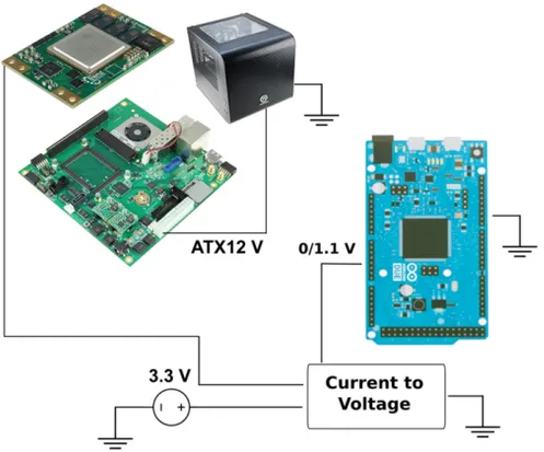
To measure only the compute module power drain, we have disabled the on-board voltage regulators which provide to the MPSoC the required 3.3V power supply. Then we provided this voltage from an external bench top power supply, monitoring the drained current with a custom DAQ system, shown in Fig.3and sampling at 20KHz. Running the FER benchmark for several iterations, while monitoring the current drain, we have been able to compute the average power drain in Watt at a sustained GFLOP/s rate, allowing us to compute the GFLOPs/Watt metric.
In particular, we measure 21.0 GFLOPs/Watt for single-precision floating-point op-erations, and 4.7 GFLOPs/Watt for double-precision ones. This highlight the fact that this hardware is not only more efficient from the performance point of view in comput-ing scomput-ingle-precision operations (≈ 2.7× faster), but is also much more energy-efficient in this condition (≈ 4.5× more energy-efficient). On the other side, the double-precision performance is less attractive, probably due to the DSP design, which has been optimized for 32-bit operations. Moreover, given the available DSPs, the implementation of double-precision operations can be obtained in different ways [17,18], with different tradeoff
Figure 3. Schema of the custom current monitoring system used to measure the power drain of the MPSoC compute module, without taking into account the whole development board power drain. The power supplying lane from the development board to the compute module has been interrupted and an external power supply is used to drive the required 3.3V. This external lane pass through an Hall effect current-voltage transducer, which can be sampled at 20KHz by the ADC of an Arduino DUE board.
between resources, area and latency, thus a further investigation would be needed to un-derstand if the default one is the optimal one form the energy-efficiency point of view.
4. Conclusions and future works
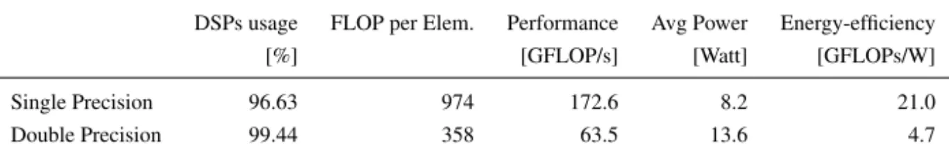
We can summarize in Tab.1all the information obtained running FER on an actual FPGA hardware (i.e., the 16nm FinFET+ XCZU9EG MPSoC), including the energy-efficiency metrics collected thank to the use of the custom DAQ system described in Sec.3.2.
From these results, we can predict that adopting such FPGA as an accelerator, sci-entific applications requiring single-precision floating-point computations, could reach a reasonable performance, but more interestingly, a high energy-efficiency.
As a comparison, Intel Broadwell CPUs released in the same period, built around 14nm technology, can reach a theoretical double-precision peak performance of ≈ 100−400 GFLOP/s, with a Thermal Design Power (TDP) of ≈ 80−160 Watt, according to the models (number of cores and core frequency), using AVX2 vector instructions5.
This translate to a performance in the same order of magnitude as the one empirically reached with the tested FPGA, but requiring a power consumption of one order of mag-nitude higher. Using FMA3 instructions Broadwell CPUs could actually reach a higher theoretical performance, but the used synthesis tool do not produce any special handling
5 https://www.microway.com/knowledge-center-articles/detailed-specifications-of-the-intel-xeon-e5-2600v4-broadwell-ep-processors/
Table 1. Results concerning the execution of the FER synthetic benchmark, compiled using OmpSs@FPGA and Vivado 2017.3 and run on the FPGA embedded in the XCZU9EG MPSoC.
DSPs usage FLOP per Elem. Performance Avg Power Energy-efficiency
[%] [GFLOP/s] [Watt] [GFLOPs/W]
Single Precision 96.63 974 172.6 8.2 21.0
Double Precision 99.44 358 63.5 13.6 4.7
of FMAs6.In the FPGA in fact each FMA is implemented as a multiplier plus an adder and given the fact that actual applications do not perform just FMAs, it seems more fair to compare to CPUs not using special FMA instructions.
Concerning scientific applications requiring double-precision floating-point compu-tations, these would enjoy a lower energy-efficiency using such FPGA as a target ac-celerator. This could be caused by the hardware architecture of the DSPs contained in the FPGA, which were not optimized for double-precision operations, but may also be related to a floating-point IP Core, used by the synthesis tools, which could be im-proved [18].
As future works we plan to further investigate the performance and energy-efficiency of this device, producing different empirical Roofline plots for different FPGA clock frequencies. We will also try to increase the double-precision performance, initially try-ing newer versions of the Xilinx Vivado tools, since the floattry-ing-point IP Core seems to be improved in the last months and also specialized implementations for FMA opera-tions seems now to be available7.We also plan to experiment software techniques, such as the use of extended-precision [19], evaluating its performance, energy-efficiency and usability for actual HPC scientific applications, wrt regular double-precision.
Moreover, we will further investigate the performance and energy-efficiency of the Arm cores [20] embedded in the same MPSoC, in order to have a full characterization of this device, assessing the possibility to share the computations between the Arm CPU and the FPGA. Eventually we plan also to provide a more comprehensive comparison with other architectures commonly adopted in the HPC field.
Acknowledgments: E.C. has been supported by the European Union’s H2020 research and innovation programme under EuroEXA grant agreement No. 754337. This work has been done in the framework of the EuroEXA EU project and of the COKA, and COSA, INFN projects. We thank Angelo Cotta Ramusino and Stefano Chiozzi, from Electronic Services of INFN Ferrara, for the help in setting up the power measuring system.
References
[1] Baity-Jesi, M., et al.: Janus II: A new generation application-driven computer for spin-system simula-tions. Computer Physics Comm. 185(2), 550 – 559 (2014),doi:10.1016/j.cpc.2013.10.019
[2] G¨uneysu, T., Kasper, T., Novotn´y, M., Paar, C., Rupp, A.: Cryptanalysis with copacobana. IEEE Trans-actions on Computers 57(11), 1498–1513 (Nov 2008),doi:10.1109/TC.2008.80
[3] Vanderbauwhede, W., Benkrid, K.: High-performance computing using FPGAs, vol. 3. Springer (2013),
doi:10.1007/978-1-4614-1791-0
6We would measure the same performance executing a generic sequence of additions and multiplications. 7 https://www.xilinx.com/support/documentation/ip_documentation/ru/floating-point.html#zynquplus
[4] Zohouri, H.R., Maruyama, N., Smith, A., Matsuda, M., Matsuoka, S.: Evaluating and optimizing opencl kernels for high performance computing with fpgas. In: SC ’16: Proceedings of the International Con-ference for High Performance Computing, Networking, Storage and Analysis. pp. 409–420 (Nov 2016),
doi:10.1109/SC.2016.34
[5] Bonati, C., Calore, E., Coscetti, S., D’Elia, M., Mesiti, M., Negro, F., Schifano, S.F., Tripiccione, R.: Development of scientific software for HPC architectures using OpenACC: the case of LQCD. In: The 2015 International Workshop on Software Engineering for High Performance Computing in Science (SE4HPCS). pp. 9–15. ICSE Companion Proceedings (2015),doi:10.1109/SE4HPCS.2015.9
[6] V´estias, M., Neto, H.: Trends of cpu, gpu and fpga for high-performance computing. In: 2014 24th International Conference on Field Programmable Logic and Applications (FPL). pp. 1–6 (Sep 2014),
doi:10.1109/FPL.2014.6927483
[7] Jin, Z., Finkel, H., Yoshii, K., Cappello, F.: Evaluation of a floating-point intensive kernel on fpga. In: Heras, D.B., Boug´e, L., Mencagli, G., Jeannot, E., Sakellariou, R., Badia, R.M., Barbosa, J.G., Ricci, L., Scott, S.L., Lankes, S., Weidendorfer, J. (eds.) Euro-Par 2017: Parallel Processing Workshops. pp. 664–675 (2018)
[8] Nurvitadhi, E., Venkatesh, G., Sim, J., Marr, D., Huang, R., Ong Gee Hock, J., Liew, Y.T., Srivatsan, K., Moss, D., Subhaschandra, S., Boudoukh, G.: Can fpgas beat gpus in accelerating next-generation deep neural networks? In: Proceedings of the 2017 ACM/SIGDA International Symposium on Field-Programmable Gate Arrays. pp. 5–14. FPGA ’17, ACM (2017),doi:10.1145/3020078.3021740
[9] Williams, S., Waterman, A., Patterson, D.: Roofline: An insightful visual performance model for multi-core architectures. Commun. ACM 52(4), 65–76 (Apr 2009),doi:10.1145/1498765.1498785
[10] Lo, Y.J., Williams, S., Van Straalen, B., Ligocki, T.J., Cordery, M.J., Wright, N.J., Hall, M.W., Oliker, L.: Roofline model toolkit: A practical tool for architectural and program analysis. In: Jarvis, S.A., Wright, S.A., Hammond, S.D. (eds.) High Performance Computing Systems. Performance Modeling, Benchmarking, and Simulation. pp. 129–148. Springer International Publishing, Cham (2015) [11] Filgueras, A., Gil, E., Alvarez, C., Jimenez, D., Martorell, X., Langer, J., Noguera, J.: Heterogeneous
tasking on SMP/FPGA SoCs: The case of OmpSs and the Zynq. In: 2013 IFIP/IEEE 21st International Conference on Very Large Scale Integration (VLSI-SoC). pp. 290–291 (Oct 2013),doi:10.1109/ VLSI-SoC.2013.6673293
[12] Bosch, J., Filgueras, A., Vidal, M., Jimenez-Gonzalez, D., Alvarez, C., Martorell, X.: Exploiting par-allelism on GPUs and FPGAs with OmpSs. In: Proceedings of the 1st Workshop on Autotuning and adaptivity approaches for energy efficient HPC Systems. p. 4. ACM (2017),doi:10.1145/3152821. 3152880
[13] Pop, A., Cohen, A.: Openstream: Expressiveness and data-flow compilation of openmp streaming pro-grams. ACM Transactions on Architecture and Code Optimization (TACO) 9(4), 53 (2013),doi: 10.1145/2400682.2400712
[14] Duran, A., Ayguad´e, E., Badia, R.M., Labarta, J., Martinell, L., Martorell, X., Planas, J.: OmpSs: a proposal for programming heterogeneous multi-core architectures. Parallel processing letters 21(02), 173–193 (2011)
[15] Calore, E., Schifano, S.F., Tripiccione, R.: Energy-performance tradeoffs for HPC applications on low power processors. Lecture Notes in Computer Science (including subseries Lecture Notes in Artificial Intelligence and Lecture Notes in Bioinformatics) 9523, 737–748 (2015), doi:10.1007/978-3-319-27308-2_59
[16] Xilinx: Zynq ultrascale+ mpsoc: Embedded design tutorial (2018), uG1209
[17] Jaiswal, M.K., Cheung, R.C.: Area-efficient architectures for double precision multiplier on FPGA, with run-time-reconfigurable dual single precision support. Microelectronics Journal 44(5), 421 – 430 (2013),
doi:https://doi.org/10.1016/j.mejo.2013.02.021
[18] Jaiswal, M.K., So, H.K.: DSP48E efficient floating point multiplier architectures on FPGA. In: 2017 30th International Conference on VLSI Design and 2017 16th International Conference on Embedded Systems (VLSID). pp. 1–6 (Jan 2017),doi:10.1109/ICVD.2017.7913322
[19] Thall, A.: Extended-precision Floating-point Numbers for GPU Computation. In: ACM SIGGRAPH 2006 Research Posters. SIGGRAPH ’06 (2006),doi:10.1145/1179622.1179682
[20] Laurenzano, M., Tiwari, A., Jundt, A., Peraza, J., Ward, W.J., Campbell, R., Carrington, L.: Character-izing the Performance-Energy Tradeoff of Small ARM Cores in HPC Computation. In: Euro-Par 2014 Parallel Processing, LNCS, vol. 8632, pp. 124–137 (2014),doi:10.1007/978-3-319-09873-9_11