Università degli Studi di Ferrara
DOTTORATO DI RICERCA IN
FISICA
CICLO XXVII
COORDINATORE Prof. VINCENZO GUIDI
Tesi in co-tutela con l’Università di Strasburgo finanziata dal Bando Vinci 2013
CORRELATION BETWEEN STRUCTURAL
AND ELECTRICAL PROPERTIES
OF ORGANIC SEMICONDUCTING MATERIALS
Settore Scientifico Disciplinare FIS/01
Dottorando Tutore
Dott. FERLAUTO LAURA Prof. GUIDI VINCENZO
Co-tutore Prof. SAMORÍ PAOLO
Referee
Prof. FRABONI BEATRICE, Università di Bologna Prof. MORGANTE ALBERTO, Università di Trieste
Prof. SCHREIBER FRANK, Università di Tubinga (Germania) Prof. RESEL ROLAND, Università di Graz (Austria)
Altri membri della commissione
Dr. SLIWA MICHEL, Università di Lille (Francia)
Dr. MdC. MAURO MATTEO, Università di Strasburgo (Francia) Dr. MILITA SILVIA, IMM-CNR di Bologna
UNIVERSITÉ DE STRASBOURG
ÉCOLE DOCTORALE DES SCIENCES CHIMIQUES
THÈSE
EN CO-TUTELLE AVEC L’UNIVERSITÉ DE FERRARA FINANCÉ PAR BANDO VINCI 2013
présentée par
Laura FERLAUTO
Soutenue le: 25 février 2015 pour obtenir le grade de
Docteur de l’Université de Strasbourg
Discipline/ Spécialité: Chimie/Physique
Correlation between structural and
electrical properties of organic
semiconducting materials
THÈSE dirigée par:
M GUIDI Vincenzo Prof., Università degli Studi di Ferrara
M SAMORÌ Paolo Prof., Université de Strasbourg
RAPPORTEURS:
Mme FRABONI Beatrice Prof., Università degli studi di Bologna
M MORGANTE Alberto Prof., Università degli studi di Trieste
EXAMINATEURS:
M MAURO Matteo Dr. MdC., Université de Strasbourg
M SILWA Michel Dr., Université de Lille
To Max and his patience. To Faby and the diplomacy which I will never learn. This thesis is as mine as yours.
A
CKNOWLEDGMENTS
These last years have been like a very intense journey full of satisfactions. The achieve-ment of this PhD represents an important milestone in my life, both from the scientific and personal point of view, which is exactly what I was looking for.
I am indebted to Prof. Guidi who let me continue the research already started at IMM-CNR of Bologna in total freedom and supported me in the realization of the co-supervision between Ferrara and Strasbourg. Also, I would like to express here my gratitude to the administrative office of the Physics Department and the Doctoral office, which helped this ”exotic case” out with all the bureaucracy of many travels and missions.
I am grateful to Prof. Samor´ı for welcoming me in his group and offering me the op-portunity to differentiate my skills at the ISIS facilities in Strasbourg. There, I learned how to face problems from other perspectives and to exchange the scientific knowledge with colleagues. The time spent with them at work and after work was priceless and the friendship that I have built with some of them will always be essential for me.
I deeply acknowledge the IMM-CNR of Bologna for welcoming me right after the Mas-ter degree and financially supporting me during the entire PhD. In particular, I want to explicitly acknowledge Dr. Milita and Dr. Liscio for the constant supervision and sugges-tions aimed to improve my work. From them I learned the importance of a scrupulous characterization of a physical system and I believe this imprinting will accompany me in future.
A big thanks goes to Prof. Biscarini’s old group at ISMN-CNR of Bologna, which was the very first big group I got in touch with. Participating to the meetings and the sci-entific discussions about the research topics studied within the group was very helpful to enlarge and enrich the view of science that I had at the beginning. Moreover, sharing every-day lab-life with other PhD students and postdocs contributed to establish pre-cious lasting friendships.
My deepest gratitude goes to all the commission members, Prof. Fraboni, Prof. Mor-gante, Dr. Mauro and Dr. Sliwa, as well as to the external referees, Prof. Resel and Prof. Schreiber, for the time they dedicated to me and my thesis. Having external scientific opinions and comments on the work I carried out is of fundamental importance for my future.
In the end, as always, I am thankful to all the people who trust and love me: my fam-ily, Max, his famfam-ily, old and new friends as well as close and very far ones. All of you contributed to make this journey amazing.
I
NDEX
Summary 1 Abstract . . . 1 Sommario . . . 5 R´esum´e . . . 9 Bibliography . . . 13 Introduction 16 Bibliography . . . 171 Charge transport properties in organic semiconducting materials 19 1.1 Organic semiconductors . . . 19 1.1.1 sp3 hybridization . . . 20 1.1.2 sp2 hybridization . . . 21 1.1.3 sphybridization . . . 21 1.1.4 Small molecules . . . 23 1.1.5 Polymers . . . 24
1.2 Charge transport models . . . 26
1.2.1 Inorganic materials: nearly free-electron model . . . 26
1.2.2 Organic materials: polarons . . . 27
1.2.2.1 Hopping model . . . 28
1.2.2.2 Variable range hopping model . . . 29
1.2.2.3 Multiple trapping and release model . . . 29
1.3 Organic field-effect transistors . . . 30
1.3.1 Ambipolar OFETs . . . 35
1.4 Interfaces in organic devices . . . 37
1.4.1 Semiconductor-metal . . . 37
1.4.2 Semiconductor-dielectric . . . 39
1.5 Correlation between structural and electrical properties . . . 40
1.6 Bibliography . . . 41
2 Fabrication techniques and characterization methods 45 2.1 Fabrication techniques . . . 45
2.1.1 Spin-coating . . . 45
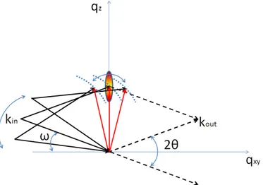
2.1.3 Organic molecular beam deposition . . . 48 2.1.4 Electrodes deposition . . . 49 2.2 Characterization methods . . . 49 2.2.1 Structural characterization . . . 50 2.2.1.1 X-ray Reflectivity . . . 50 2.2.1.2 X-ray diffraction . . . 54 2.2.1.3 Specular scan . . . 57 2.2.1.4 Rocking curve . . . 58
2.2.1.5 Grazing Incidence X-ray Diffraction . . . 59
2.2.1.6 Laboratory source vs synchrotron . . . 60
2.2.2 Morphological characterization . . . 64
2.2.3 Electrical characterization . . . 66
2.2.4 Optical characterization . . . 66
2.3 Bibliography . . . 67
3 A comparative study on OFETs based on two perylene di-imide derivatives 69 3.1 Introduction . . . 69 3.2 Experimental . . . 69 3.2.1 Active Materials . . . 69 3.2.2 Device fabrication . . . 70 3.2.3 Characterization methods . . . 70 3.2.3.1 Structural characterization . . . 70 3.2.3.2 Morphological characterization . . . 71 3.2.3.3 Electrical characterization . . . 71
3.3 Results and discussion . . . 71
3.3.1 The structures of the bulk . . . 71
3.3.2 The structures of the films . . . 72
3.3.2.1 Grazing incidence X-ray diffraction . . . 72
3.3.2.2 Rocking curves . . . 75
3.3.2.3 X-ray reflectivity . . . 76
3.3.3 The morphology of the films . . . 78
3.3.4 Transport properties of the films . . . 80
3.3.4.1 Evaluation of the HOMO and LUMO levels . . . 80
3.3.4.2 Electrical results on not-functionalized electrodes . . . 81
3.3.4.3 Electrical results on functionalized electrodes . . . 85
3.4 Conclusions . . . 87
iii 4 Ambipolar OFETs based on solution processed polymeric bilayers 91
4.1 Introduction . . . 91
4.2 Experimental . . . 92
4.2.1 Active Materials . . . 92
4.2.2 Device fabrication . . . 92
4.2.3 Characterization methods . . . 93
4.2.3.1 X-ray diffraction measurements . . . 93
4.2.3.2 X-ray reflectivity measurements . . . 94
4.2.3.3 Morphological characterization . . . 94
4.2.3.4 Electrical characterization . . . 94
4.3 Results and discussion . . . 94
4.3.1 The single N2200 layer . . . 94
4.3.1.1 Crystalline structure . . . 94
4.3.1.2 X-ray reflectivity . . . 97
4.3.1.3 Morphology . . . 97
4.3.1.4 Electrical properties . . . 98
4.3.2 The single IIDDT-C3 layer . . . 100
4.3.2.1 Morphology . . . 100 4.3.2.2 Crystalline structure . . . 100 4.3.2.3 X-ray reflectivity . . . 103 4.3.2.4 Electrical behavior . . . 103 4.3.3 The bilayers . . . 104 4.3.3.1 Crystalline structure . . . 105 4.3.3.2 Morphology . . . 107 4.3.3.3 Electrical properties . . . 107 4.4 Conclusions . . . 117 4.5 Bibliography . . . 118
5 In-situ and real-time study on pentacene OFETs 121 5.1 Introduction . . . 121 5.2 Experimental . . . 121 5.2.1 Active materials . . . 121 5.2.2 Device fabrication . . . 121 5.2.3 Characterization methods . . . 122 5.2.3.1 Structural characterization . . . 122 5.2.3.2 Morphological characterization . . . 123 5.2.3.3 Electrical characterization . . . 123
5.3 Results and discussion . . . 123
5.3.1 Effect of X-ray beam on OFET response . . . 124
5.3.3 Effect of the electric field on the out-of-plane diffraction peaks . . . 127
5.3.4 Effect of the electric field on the in-plane diffraction peaks . . . 130
5.3.5 Computational studies . . . 131
5.4 Conclusions . . . 133
5.5 Bibliography . . . 133
6 In-situ and real time-structural study on humidity sensitive organic thin films 135 6.1 Introduction . . . 135
6.2 Experimental . . . 136
6.2.1 Active materials . . . 136
6.2.2 Thin-film fabrication . . . 137
6.2.3 Experimental setup for in-situ structural investigation . . . 137
6.3 Results and discussion . . . 138
6.4 Conclusions . . . 140
6.5 Bibliography . . . 140
S
UMMARY
Abstract
The need of low-cost and large-area applications compatible with flexible substrates has guided the scientific community to the design of new organic semiconducting materials characterized by high solubility in common solvents, good air stability and high charge carrier mobility for organic field effect transistors (OFETs) devices, the building blocks of organic electronics. The success of this generation of π-conjugated materials is principally related to the improved physical understanding of their structure-properties relationship. The material microstructure, that is its crystalline structure, its molecular packing, the orientation and arrangement of the molecules on a substrate, the formation of crystalline domains as well as the presence of disorder and defects, has in fact a strong influence on the charge transport taking place in the OFET [1, 2]. To unravel the relationship linking the structural and electrical properties of several organic semiconducting materials, small molecules and polymers, characterized by different degrees of crystalline order is the aim of this thesis. OFETs can be fabricated exploiting a variety of architectures and organic materials deposited either by solution based techniques or vacuum sublimation. Thanks to the high degree of crystalline order and large homogeneity, vacuum sublimated de-vices are largely studied as model-systems for the comprehension of the organic semi-conductor physics. Even though more attractive for inexpensive applications, solution based devices presents less crystaline order with respect to vacuum sublimated ones and their deep investigation still represents a challenge. Two basic approaches for the nves-tigation of the relationship between structural and electrical properties of some organic materials were adopted in this thesis: ex-situ multiple characterization and in-situ and real-time structural investigation.
The ex-situ characterization (structural, morphological, electrical, optical, etc.) of the system at the equilibrium is one of the most common approaches in literature. In this thesis it has been exploited to investigate OFETs based on two perylene derivatives as well as on ambipolar transistors fabricated with solution processable n-type and p-type polymers deposited with a particular technique. Among n-type organic semiconductors, perylene alkyldiimide derivatives (PDIs) were chosen for their good electrical perfor-mance as well as excellent processability. [3, 4]. In particular,we studied PDIs exhibiting a core functionalized with cyano-groups, which lower the lowest unoccupied molecu-lar orbital energy [5, 6] improving the air stability, and side chains, which increment the solubility and thus the material processability. The introduction of side chains in
π-conjugated molecules also affects the extent of molecular order and consequently the efficiency of charge transport in the material and it is this aspect that we investigated. OFETs based on spin-coated thin films of dicyanoperylene molecules decorated with either linear (PDI8-CN2 - N,N’-bis(n-octyl)-dicyanoperylene-3,4:9,10-bis-dicarboximide) or branched (N1400 - N,N’-bis-(2-ethylhexyl)-1,7-dicyano-perylene-3,4:9,10-bis (dicarbox-imide)) side chains were studied to elucidate the role of the alkyl chins shape on the struc-ture of the thin films and consequently on the device performance. The results demon-strate that in PDI derivatives the introduction of asymmetric branched alkyl chains al-lows obtaining, upon thermal annealing, OFETs with enhanced transport properties with respect to linear alkyl chains. The branched specie leads to the formation of films consist-ing on a mixture of four stereoisomers, two RR/SS and RS/SR enantiomeric pairs which introduce conformational disorder favoring the 2D-growth mode. For these molecules optimized post-deposition thermal annealing leads to a structural transition towards the bulk-phase, still preserving the 2D morphology and improving the transport properties of thin film devices. Conversely, molecules with linear alkyl chains self-assemble in stable 3D islands exhibiting the bulk phase structure which keep their size constant without ma-jor changes in the OFETs characteristics upon thermal treatment. These results show how the substitution of a dicyanoperylene molecule with asymmetric branched alkyl chains can be an effective strategy for obtaining, just after simple thermal annealing, field-effect transistors with enhanced transport properties with respect to linear alkyl chains. More-over, these findings demonstrate that the disorder generated by the asymmetric branched chains when the molecule is physisorbed in thin film can be instrumental for enhancing charge transport via thermal annealing [7].
The second ex-situ study concerns the characterization of bilayer ambipolar OFETs based on multiple-layers of n-type and p-type polymeric thinfilms deposited by Langmuir-Schaefer (LS) technique. The production of ambipolar OFETs with high and balanced electron-hole mobilities is currently a research highlight due to their potential applica-tion in organic integrated circuits. The possibility of obtaining a simultaneous transport of both types of carriers would not only lead to a simplification in the design of com-plementary logic circuits, but would also reduce power dissipation and increase noise margins. The LS technique permits the fabrication of an ambipolar device by the consec-utive deposition of both n- and p-type layers from solutions. This method involves the creation of a single monolayer thick film by spreading a solution at the water-air interface and then transferring it by gently putting in contact a solid substrate with the film floating on the water surface [8]; the procedure can be performed just one time if a single mono-layer is needed or many times if multiple mono-layers have to be deposited. This technique enables an accurate control over the film thickness and favors a strong molecular packing and long-range order in the structure of the deposited layer. Generally, charge mobility in polymeric devices suffers from poor packing and lack of microscopic order induced by the polymer conformation itself and the presence of long alkyl chains which create a
3
relevant steric hindrance [9]. With respect to other deposition techniques from solution, the LS method forces the polymer packing in an advantageous configuration for charge transport. For this particular study, IIDDT-C3, a promising isoindigo-based conjugated p-type polymer, was chosen for exceptionally high electrical performance and good crys-talline order already reached by spin-coating technique [10] together with P(NDI2OD-T2) (or N2200), a commercial outstanding n-type polymer, which has already demonstrated high electrical response both in spin-coated and LS thin-films [11–14]. After choosing optimal deposition conditions for the n-type and p-type materials, single layers and bi-layers composed by the superposition of N2200 and IIDDT-C3 (and vice versa) were structurally characterized. Grazing incidence X-ray diffraction measurements provided necessary information about the effect of the deposition technique onto the crystalline order and molecular packing of the organic layers. Single p- and n-type layers showed an edge-on arrangement of the polymeric lamella with respect to the surface which was maintained also in the ambipolar architectures and enabled to reach remarkable holes (µh) and electrons (µe) mobility, with values in saturation regime of the order of 10−1. Moreover, the IIDDT-C3 layer showed a fiber-like organization induced by the LS depo-sition technique further proved by atomic force microscopy images.
The approach based on the in-situ and real-time structural investigation is the most appropriate one to describe the structural evolution of a system under not equilibrium circumstances. It implies that the structural characterization is performed exactly during the system response to an external stimulus. Despite the tremendous amount of phys-ical information that can be extrapolated, this approach is not very common due to the experimental complexity of following fast evolving phenomena. This strategy has been exploited in this thesis to study the effect of the electric field on the structure of evap-orated pentacene in working OFET as well as to follow the structural evolution of thio-phene derivative thin films for humidity sensor applications during the relative humidity variation in the environment. As already known in literature [15–17], in OFETs charge transport is strongly influenced by the structure and morphology of the organic film at the interface with the dielectric. Nevertheless, the structural changes in the organic semi-conducting layer induced by the electric field drifting the charge carriers from the source to the drain electrode are still unknown. In-situ and real-time X-Ray diffraction mea-surements using a synchrotron radiation source, both in specular and grazing incidence geometries, were thus performed on pentacene-based OFETs to elucidate the structural evolution of the organic material during the application of gate (VSG) and source-drain
(VSD) bias. Ad-hoc bottom-gate top-contact OFETs suitable for the realization of X-ray
measurements inside the device channel were fabricated. Although very small (few mrad), it was possible to demonstrate for the first time the occurrence of a lattice ex-pansion due to the tilt of pentacene molecules during the VSG and VSD application. The
result is reversible and supported by molecular dynamics and DFT simulations.
ap-plications [18–21]. Samples constituted by a thin TTF-based conductive layer on top of a polymeric matrix were supplied by the group of Professor Rovira (ICMAB-CSIC, Spain). A home-made humidity chamber adapted for simultaneous X-rays and electrical mea-surements in a controlled atmosphere was built and set on the goniometer of the labo-ratory diffractometer. The chamber was connected to a hygrometer probe and to a gas tube, through which a hydrate nitrogen flux was inflated, in order to reach the desired relative humidity (RH%). Two kapton windows allowed the X-ray incident beam to reach the sample positioned inside the chamber and the reflected/diffracted beam to reach the detector. This setup allowed for the X-ray analysis of some characteristic peaks of the material during RH% variation. The results demonstrated that the variation of RH% re-versibly affects the thin-film structure; in particular a lattice expansion was correlated to the increment of RH%, suggesting that water molecules penetrate inside the crystallites modifying the lattice parameters.
In conclusion, in this thesis examples of multi-technique approach as well as in-situ and real-time structural investigations on different organic semiconducting materials are presented. In both cases, the multiscale study of the close interconnection between struc-tural, morphological and electrical properties of a system brought to a comprehensive description of the materials themselves and of the devices based on them.
This manuscript presents the results of a 3 years Ph.D. work in co-supervision be-tween the University of Ferrara and the University of Strasbourg under the financial support of the French-Italian University with the Bando Vinci 2013. The work has been mainly carried out at the Istituto di Microelettronica e Microsistemi of the Consiglio Nazionale delle Ricerche (IMM-CNR) of Bologna (Italy) and at the Institut de Science et d’Ing´enierie Supramol´eculaires (ISIS) of Strasbourg (France).
5
Sommario
La necessit`a di produrre applicazioni dai costi contenuti, capaci di coprire grandi super-fici e compatibili con substrati flessibili, ha guidato la comunit`a scientifica verso la proget-tazione di nuovi materiali organici caratterizzati da elevata solubilit`a in solventi comuni, buona stabilit`a in aria ed alta mobilit`a dei portatori di carica in transistori ad effetto di campo (OFETs), i mattoni dell’ elettronica organica. Il successo di questa generazione di materiali π-coniugati `e principalmente legato ai miglioramenti nella comprensione della fisica del legame struttura-propriet`a nei materiali stessi. La microstruttura del materi-ale, ovvero la sua struttura cristallina, l’orientazione ed organizzazione delle molecole su di un substrato, la formazione di domini cristallini, nonch´e la presenza di disordine e difetti, ha infatti una forte influenza sul trasporto di carica nel corrispettivo OFET [1, 2]. Lo scopo di questa tesi `e di chiarire la relazione tra le propriet`a strutturali ed elettriche di materiali semiconduttori organici, piccole molecole e polimeri, caratterizzati da differ-enti gradi d’ordine cristallino. Gli OFETs possono essere fabbricati sfruttando una variet`a d’architetture e materiali organici depositati sia mediante tecniche da soluzione, sia me-diante sublimazione in ultra-alto vuoto. Grazie all’elevato grado d’ordine cristallino ed omogeneit`a, dispositivi basati su molecole organiche sublimate sono ampiamente stu-diati come sistemi-modello per la comprensione della fisica del dispositivo. I dispositivi fabbricati mediante processi di deposizione da soluzione, nonostante siano pi `u attraenti per applicazioni a basso costo, presentano un basso ordine cristallino e l’indagine appro-fondita dei loro meccanismi di trasporto rappresenta ancora una sfida. In questa tesi sono stati adottati due approcci per investigare la relazione tra struttura e propriet`a elettriche di alcuni materiali organici: caratterizzazione multipla ex-situ ed indagine strutturale in-situ in tempo reale.
La caratterizzazione ex-situ (strutturale, morfologica, elettrica, ottica, ecc) di un sis-tema `e uno degli approcci pi `u comuni in letteratura. In questa tesi `e stata sfruttata per indagare OFETs basati su due derivati perilenici oltre che transistori ambipolari fabbri-cati depositando strati multipli di polimeri di tipo n e p mediante una particolare tecnica da soluzione.
Tra i semiconduttori organici di tipo n, sono stati scelti i derivati del perilene alkyldi-imide (PDIs) per le loro buone prestazioni elettriche e l’ottima processabilit`a [3, 4]. In particolare sono stati studiati derivati del PDI il cui core `e funzionalizzato con gruppi ciano che abbassano l’energia del pi `u basso orbitale molecolare non occupato incremen-tando la stabilit`a in aria [5, 6] e con catene laterali in grado di aumentare la solubilit`a emigliorare quindi la processabilit`a. La presenza di di catene laterali influisce anche sul grado d’ordine molecolare del film e di conseguenza sull’efficienza del trasporto di carica nel materiale. OFETs basati su film sottili di derivati del PDI decorati con catene lineari (PDI8-CN2 - N,N’-bis(n-octyl)-dicyanoperylene-3,4:9,10-bis-dicarboximide) e ramificatie (N1400 - N,N’-bis-(2-ethylhexyl)-1,7-dicyano-perylene-3,4:9,10-bis(dicarboximide)) sono
stati studiati per stabilire il ruolo della forma delle catene alchiliche sulla struttura dei film sottili e di conseguenza sulle prestazioni elettriche del dispositivo. I risultati tenuti dimostrano che l’introduzione di catene ramificate asimmetriche permette di ot-tenere, con un opportuno trattamento termico, OFETs con migliori prestazioni elettriche rispetto a quelle lineari. Il composto a catene ramificate `e costituito da una miscela di quattro stereoisomeri, ovvero le due coppie enantiomeriche RR/SS e RS/SR, che sono presenti nel film ed inducono un disordine conformazionale da cui dipende la morfolo-gia bidimensionale. Per queste molecole un trattamento termico ottimizzato a seguito della deposizione porta ad una transizione strutturale verso la fase di bulk, conservando la morfologia 2D e migliorando le propriet`a di trasporto dei dispositivi. Al contrario, le molecole con catene alchiliche lineari auto-assemblano in isole 3D caratterizzate dalla fase bulk pi `u stabile e mantengono le loro caratteristiche pressoch´e inalterate anche dopo il trattamento termico. Questi risultati mostrano come in un derivato del PDI la sosti-tuzione di catene alchiliche lineari con catene asimmetriche ramificate possa essere una strategia efficace per ottenere, a seguito di un semplice trattamento termico, transistori ad effetto di campo con migliori propriet`a di trasporto. Inoltre, questi risultati dimostrano che il disordine generato dalle catene asimmetriche ramificate quando la molecola viene fisisorbita su una superficie pu `o essere decisivo per il miglioramento del trasporto di carica [7].
Il secondo studio ex-situ riguarda la caratterizzazione di OFETs ambipolari basati su pi `u strati di polimeri di tipo n e p depositati mediante la tecnica Langmuir-Schaefer (LS). La produzione di OFETs ambipolari con mobilit`a elettrone-lacuna elevate e comparabili `e attualmente un tema d’interesse a causa della loro potenziale applicazione in circuiti integrati organici. La possibilit`a di ottenere un trasporto simultaneo di entrambi i tipi di portatori porterebbe non solo ad una semplificazione nella progettazione di circuiti logici complementari, ma servirebbe anche a ridurre la dissipazione di potenza ed au-mentare i margini di rumore dei dispositivi. La tecnica LS permette la fabbricazione di un dispositivo ambipolare mediante la deposizione consecutiva di entrambi gli strati n e p da soluzione. Questo metodo comporta la creazione di un monostrato di film per diffusione della soluzione all’interfaccia acqua-aria ed il trasferimento dello stesso su di un substrato solido [8]; la procedura pu `o essere eseguita una volta sola, se un singolo monostrato `e necessario oppure diverse volte se devono essere depositati strati multipli. Questa tecnica permette un controllo accurato dello spessore e la struttura dello starto depositato favorendo un forte impacchettamento molecolare nonch`e ordine a lungo rag-gio. In generale, la mobilit`a dei portatori di carica in dispositivi polimerici `e ridotta a causa dello scarso impacchettamento e mancanza di ordine indotto dalla conformazione del polimero stesso e dalla presenza di catene alchiliche lunghe che creano un rilevante ingombro sterico [9]. Rispetto ad altre tecniche di deposizione da soluzione, il metodo LS costringe il polimero ad impacchettarsi ed organizzarsi sulla superficie in una config-urazione vantaggiosa per il trasporto di carica. In particolare per questo studio `e stato
7
scelto l’ IIDDT-C3, un polimero π-coniugato di tipo p derivato dell’isoindigo, per le ec-cezionali prestazioni elettriche e buon ordine cristallino gi`a ottenibile mediante depo-sizione dd spin-coating [10]. All’IIDDT-C3 `e stato affiancato P(NDI2OD-T2) (o N2200), un eccezionale polimero commerciale di tipo n, che ha gi`a dimostrato buone risposte elettriche in film sottili preparati sia per spin-coating che LS [11–14]. Dopo aver deter-minato le condizioni ottimali per la deposizione degli strati polimerici, singoli e multi-pli strati composti dalla sovrapposizione di N2200 e IIDDT-C3 (e viceversa) sono stati caratterizzati strutturalmente. La diffrazione da raggi X ad incidenza radente ha for-nito le informazioni necessarie per comprendere l’effetto della tecnica di deposizione sull’ordine cristallino e l’impacchettamento molecolare degli strati organici. I singoli strati di entrambi i polimeri mostrato infatti un’organizzazione edge-on (rispetto alla superficie del substrato) delle lamelle polimeriche che viene mantenuta anche nelle ar-chitetture ambipolari e che ha permesso di raggiungere mobilit`a di elettroni (µe) e lacune (µh) dell’ordine di 10−1 cm2/Vs in regime di saturazione. Inoltre, lo strato di IIDDT-C3 mostra un’organizzazione fibrillare indotta dalla tecnica di deposizione LS, ulteriormente dimostrato da immagini di microscopia a forza atomica (AFM).
L’approccio basato sull’indagine strutturale in-situ ed in tempo reale `e il metodo pi `u adatto per descrivere l’evoluzione strutturale di un sistema in situazioni di non equilib-rio. Ci `o implica che la caratterizzazione strutturale viene eseguita esattamente durante la risposta del sistema ad uno stimolo esterno. Nonostante l’enorme quantit`a di infor-mazioni fisiche che possono fornire, questo approccio non `e molto comune a causa della complessit`a sperimentale necessaria per seguire fenomeni che evolvono in scale di tempi molto ridotte. Questa strategia `e stata sfruttata in questa tesi per studiare l’effetto del campo elettrico sulla struttura di film di pentacene durante il funzionamento del OFET e per seguire l’evoluzione strutturale di film sottili basati su derivati del TTF (tetrathiaful-valene) durante la variazione dell’umidit`a relativa nell’ambiente circostante.
Come gi`a noto in letteratura [15–17], negli OFETs il trasporto di carica `e fortemente influenzato dalla struttura e morfologia del film organico all’interfaccia con il dielettrico. Tuttavia, quale sia la risposta strutturale dello strato semiconduttivo all’applicazione del campo elettrico rappresenta ancora un quesito irrisolto. Misure di diffrazione da raggi X in-situ ed in tempo reale utilizzando una sorgente di radiazione di sincrotrone sono state quindi effettuate su OFETs di pentacene per investigare l’evoluzione strutturale del mate-riale organico durante l’applicazione simultanea del potenziale di gate (VSG) e di
source-drain (VSD). OFETs con geometria bottom-gate top-contact specificatamente fabbricati
per la realizzazione di misure raggi X all’interno del canale del dispositivo sono stati utilizzati. Con questa tecnica `e stato possibile rivelare per la prima volta un’espansione reticolare del pentacene causata dall’ inclinazione delle molecole (pochi mrad) a seguito dell’applicazione di VSG e VSD. Questo fenomeno `e reversibile e supportato da
simu-lazioni di dinamica molecolare e DFT.
sen-soristiche [18–21]. I campioni costituiti da uno strato conduttore sottile su di una ma-trice polimerica sono stati forniti dal gruppo della Professoressa Rovira (ICMAB-CSIC, Spagna). Una camera per l’umidit`a adatta per effettuare misure di raggi X in simultanea con misure elettriche in atmosfera di umidit`a controllata `e stata costruita e collocata sul goniometro del diffrattometro in laboratorio. Due finestre di kapton permettono al fas-cio di raggi X incidente di raggiungere il campione posizionato al centro della camera ed a quello scatterato di raggiungere il rilevatore. Questa configurazione ha consentito l’analisi di alcuni picchi caratteristici del materiale durante la variazione di umidit`a rela-tiva (RH%) all’interno della camera monitorata da un termoigrometro. I risultati hanno dimostrato che la variazione di RH% influisce reversibilmente sulla struttura del film sottile: in particolare l’espansione reticolare correlata all’incremento di RH% suggerisce che le molecole d’acqua penetrano all’interno dei cristalliti modificandone i parametri reticolari.
In conclusione, in questa tesi vengono presentati esempi di multi-caratterizzazione ex-situ cos`ı come indagini strutturali in-situ ed in tempo reale su diversi materiali semi-conduttori organici. In entrambi i casi, lo studio della stretta interconnessione tra pro-priet`a strutturali, morfologiche ed elettriche dei sistemi ha portato ad una descrizione approfondita dei materiali stessi e dei dispositivi basati su di essi.
Questo manoscritto presenta i risultati di un dottorato di ricerca di 3 anni in co-tutela tra l’Universit`a di Ferrara e l’Universit`a di Strasburgo con il supporto finanziario dell’Universit`a Italo-Francese (Bando Vinci 2013). Il lavoro `e stato svolto principalmente presso l’Istituto di Microelettronica e Microsistemi del Consiglio Nazionale delle Ricerche (IMM-CNR) di Bologna (Italia) e presso l’Istitut de Science et d’Ing´enierie Supramol´eculaires (ISIS) di Strasburgo (Francia).
9
R´esum´e
Le besoin d’applications `a faible co ˆut et de grande surface compatibles avec des substrats flexibles a conduit la communaut´e scientifique `a la conception de nouveaux mat´eriaux semi-conducteurs organiques caract´eris´e par une solubilit´e ´elev´ee dans les solvants clas-siques, une bonne stabilit´e `a l’air et une mobilit´e de porteur de charge ´elev´ee pour les transistors organique `a effet de champ (OFET), les briques ´el´ementaires pour l’´electronique organique. Le succ`es de cette g´en´eration de mat´eriaux π-conjugu´es est principalement li´e `a la meilleure compr´ehension physique de la relation entre leur structure et leurs pro-pri´et´es. La microstructure du mat´eriau, c’est-`a-dire sa structure cristalline, l’orientation et l’arrangement des mol´ecules sur le substrat, la formation de domaines cristallins ainsi que la pr´esence de d´esordre et de d´efauts, ont en effect une forte influence sur le trans-port de charge qui prend place dans le OFET [1, 2]. Le but de cette th`ese est d’´elucider la relation reliant les propri´et´es structurales et ´electriques de plusieurs mat´eriaux semi-conducteurs organiques caract´eris´es par diff´erents degr´es d’ordre cristallin. Les OFETs peuvent ˆetre fabriqu´es en exploitant une vari´et´e d’architectures et des mati`eriaux or-ganiques d´epos´es soit par des techniques en solution, soit par sublimation sous vide. Grˆace `a un ordre cristallin ´elev´e et une grande homog´en´eit´e, les dispositifs obtenus par sublimation sous vide sont largement ´etudi´e pour la compr´ehension de la physique des semi-conducteurs organique. Mˆeme s’ils sont plus attrayant pour des applications peu co ˆuteuses, les dispositifs obtenus par solution pr´esentent un ordre cristallin moindre par rapport `a ceux obtenus par sublimation sous vide, et leur ´etude approfondie repr´esente toujours un d´efi. Deux approches de base ont ´et´e adopt´ees dans cette th`ese pour ´etudier la relation entre les propri´et´es structurale et ´electriques de mat´eriaux organique: la car-act´erisation ex-situ multiple et l’´etude structurale in situ et en temps r´eel.
La caract´erisation multiple ex situ (structural, morphologique, ´electrique, optique, etc.) du syst`eme `a l’´equilibre est l’une des plus courantes dans la litt´erature. Dans cette th´ese, elle a ´et´e exploit´ee pour ´etudier les OFETs bas´es sur deux d´eriv´es de p´eryl`ene ainsi que sur les transistors ambipolaires fabriqu´es avec des polym`eres de type n et p en solution d´epos´es par une technique particuli`ere.
Parmi les semi-conducteurs organiques de type n, les d´eriv´es de p´eryl`ene alkyldi-imide pr´esentent de bonnes performances ´electriques ainsi qu’une excellente process-abilit´e [3, 4]. Il est int´eressant de noter que les PDI peuvent ´egalement pr´esenter une bonne stabilit´e `a l’air lorsque le noyau p´eryl`ene est fonctionnalis´e par des groupes cyano, via l’abaissement de l’´energie de l’orbitale mol´eculaire vacante la plus basse [5, 6]. L’introduction de chaˆınes lat´erales dans les mol´ecules π-conjugu´ees est une strat´egie largement utilis´ee pour augmenter leur solubilit´e et ainsi am´eliorer leur processabilit´e pour des dispositifs `a couches minces, mais elle affecte aussi l’´etendue de l’ordre mol´eculaire et par cons´equent l’efficacit´e du transport de charges dans le mat´eriau. Nous avons ´etudi´e des couches minces obtenues par spin-coating de mol´ecules de dicyanoperylene
d´ecor´ees avec des chaˆınes lat´erales lin´eaires (PDI8-CN2 - N, N’-bis (n-octyl) -dicyanoperylene-3,4: 9,10-bis-dicarboximide) ou ramifi´ees (N1400 - N, N’-bis- (2-´ethylhexyl) -1,7-dicyano-p´eryl`ene-3,4: 9,10-bis (dicarboximide)) afin d’´elucider le r ˆole des chaˆınes alkyle sur la structure des couches minces et par cons´equent sur les performances du dispositif. En effet, l’introduction de chaˆınes alkyle ramifi´ees asym´etriques dans les d´eriv´es de PDI permet d’obtenir apr`es traitement thermique des OFET avec des propri´et´es de trans-port am´elior´ees par raptrans-port `a des chaˆınes alkyle lin´eaires. Nous avons montr´e que l’esp`ece ramifi´ee conduit `a la formation de films constitu´es d’un m´elange de quatre st´er´eoisom`eres, `a savoir deux paires d’´enantiom`eres RR/SS et RS/SR, et seul ce d´esordre conformationnel favorise le mode croissance 2D. Pour ces mol´ecules, un traitement ther-mique post-d´ep ˆot optimis´e conduit `a une transition structurale vers la phase bulk, tout en pr´eservant la morphologie 2D et en am´eliorant les propri´et´es de transport des dispositifs `a couches minces. Inversement, les mol´ecules avec des chaˆınes alkyle lin´eaires s’auto-assemblent dans des ˆılots 3D stables pr´esentant la structure de la phase bulk qui gar-dent leur taille constante sans changements majeurs dans les caract´eristiques des OFET apr`es traitement thermique. Ces r´esultats montrent comment la fonctionnalisation d’une mol´ecule de dicyanop´eryl`ene avec des chaˆınes alkyle ramifi´ees asym´etriques peut ˆetre une strat´egie efficace pour obtenir, apr`es un simple traitement thermique, des transistors `a effet de champ avec des propri´et´es am´elior´ees de transport par rapport `a des chaˆınes alkyle lin´eaires. En outre, ces r´esultats montrent que lorsque la mol´ecule est physisorb´ee en couches minces, le d´esordre g´en´er´e par les chaˆınes ramifi´ees asym´etriques peut con-tribuer `a l’am´elioration du transport de charges par traitement thermique [7].
Une autre ´etude ex-situ concerne la caract´erisation d’OFET ambipolaires bicouches `a base de plusieurs couches minces de polym`eres de type n et p d´epos´ees par la tech-nique de Langmuir-Schaefer (LS). De nombreuses ´etudes s’int´eressent actuellement `a la production d’OFET ambipolaires avec des mobilit´es d’´electrons et de trous ´elev´ees et ´equilibr´ees en raison de leur potentiel d’application dans les circuits int´egr´es organiques. La possibilit´e d’obtenir un transport simultan´e des deux types de transporteurs con-duirait non seulement `a une conception simplifi´ee de circuits logiques compl´ementaires, mais permettrait ´egalement de r´eduire la dissipation de puissance et d’accroˆıtre les marges de bruit. La technique de LS permet la fabrication d’un dispositif ambipolaire par d´ep ˆot cons´ecutif de couches de type n et p en solution. Ce proc´ed´e implique la formation d’un film monocouche ´epais par dispersion d’une solution `a l’interface eau-air, puis de son transfert en mettant doucement en contact un substrat solide avec le film flottant `a la sur-face de l’eau [8]; la proc´edure peut ˆetre effectu´ee une seule fois si une monocouche est voulue ou r´ep´et´ee plusieurs fois si plusieurs couches doivent ˆetre d´epos´ees. Cette tech-nique permet un contr ˆole pr´ecis du d´ep ˆot qui produit un arrangement mol´eculaire dense et un ordre `a longue distance. La mobilit´e des charges dans les dispositifs polym`eres souffre d’un mauvais arrangement et de l’absence d’ordre microscopique induits par la conformation du polym`ere lui-mˆeme et de la pr´esence de longues chaˆınes alkyle qui
11
cr´eent un encombrement st´erique important [9]. Par rapport `a d’autres techniques de d´ep ˆot en solution, la m´ethode de LS permet de contraindre le polym`ere `a s’organiser sur la surface de mani`ere benefique pour le transport de charges. Pour cette ´etude en particulier, un polym`ere conjugu´e prometteur de type p d´eriv´e de l’isoindigo (IIDDT-C3) a ´et´e choisi pour ses performances ´electriques exceptionnellement ´elev´ees et pour le remarquable ordre cristallin d´ej`a obtenu par la technique de spin-coating [10], et un re-marquable polym`ere de type n commercial (P(NDI2OD-T2 ou N2200) qui a d´ej`a montr´e une r´eponse ´electrique ´elev´ee dans des couches minces obtenus aussi bien par spin-coating que par LS [11–14]. Apr`es avoir choisi les conditions optimales de d´ep ˆot pour les mat´eriaux de type n et p, des monocouches et des bicouches obtenues par super-position de N2200 et de IIDDT-C3 (et vice versa) ont ´et´e caract´eris´ees structurellement. Les mesures de diffraction des rayons X en incidence rasante (GIXRD) ont fourni des in-formations importantes sur l’influence de la technique de d´ep ˆot sur l’ordre cristallin et l’arrangement mol´eculaire des couches organiques. Les monocouches de type p et n ont montr´e un arrangement edge-on des lamelles de polym`ere par rapport `a la surface qui est conserv´e dans les architectures ambipolaires, ce quia permis d’obtenir des mobilit´es de trous (µh) et d’´electrons (µel) remarquables, avec des valeurs respectives de l’ordre de 10−1-10−2 cm2/Vs en r´egime de saturation. De plus, la couche d’IIDDT-C3 pr´esente
une structure en fibres r´esultant de la technique de d´ep ˆot LS qui a ´et´e confirm´ee par les images de microscopie `a force atomique.
L’approche bas´ee sur l’´etude structurale in-situ et en temps r´eel est la plus appropri´ee pour d´ecrire l’´evolution structurelle d’un syst`eme hors ´equilibre. Cela implique que la caract´erisation structurale soit effectu´ee exactement pendant la r´eponse du syst`eme `a un stimulus exterieur. Malgr´e l’´enorme quantit´e d’informations physique qui peuvent ˆetre extrapol´ees, cette approche est atypique en raison de la complexit´e exp´erimentale du suivi de ph´enom`enes rapides. Cette strat´egie a ´et´e exploit´e dans cette th`ese pour ´etudier l’effet du champ ´electrique sur la structure de pentac`ene ´evapor´e dans des OFET en fonctionnement, ainsi que pour suivre l’´evolution structurelle des couches minces de d´eriv´es de thioph`ene au cours de la variation de l’humidit´e relative de l’environnement pour des applications de capteurs d’humidit´e.
D’apr`es la litt´erature [15–17], il est connu que le transport de charges dans ces dis-positifs est fortement influenc´e par la structure et la morphologie de la couche organique `a l’interface avec le di´electrique. Toutefois, les changements structurels dans la couche semi-conductrice organique induits par le champ ´electrique faisant d´eriver les porteurs de charge de la source au drain demeurent inconnus. Des mesures de diffraction des rayons X in-situ en temps r´eel en utilisant une source de rayonnement synchrotron, `a la fois dans g´eom´etries d’incidence sp´eculaires et rasantes, ont ainsi ´et´e effectu´ees sur des OFET `a base de pentac`ene pour ´elucider l’´evolution de la structure du mat´eriau organique au cours de l’application de tensions de gate (VSG) et source-drain (VSD).
du canal des dispositifs ont ´et´e fabriqu´es. Bien que tr`es petite (quelques mrad), il a ´et´e possible de mettre en ´evidence pour la premi`ere fois une extension du r´eseau en rai-son de l’inclinairai-son des mol´ecules de pentac`ene lors de l’application de VSGet VSD. Ce
r´esultat, qui est r´eversible et appuy´e par les simulations par dynamique mol´eculaire et par la th´eorie de la fonctionnelle de la densit´e, am´eliore non seulement la description du m´ecanisme de transport de charges dans les mat´eriaux organiques, mais a aussi le potentiel d’apporter des am´eliorations futures dans le dispositif organique.
Les mati`eriaux organiques `a base t´etrathiafulval`ene (TTF) sont largement ´etudi´es pour des applications de d´etection [18–21]. Les ´echantillons constitu´es d’une mince couche conductrice `a base TTF sur une matrice polym`ere ont ´et´e fournis par le groupe du Professeur Rovira (ICMAB-CSIC, Espagne). Une chambre d’humidit´e, adapt´ee aux mesures aux rayons X et ´electriques simultan´ees dans une atmosph`ere contrˆl´ee, a ´et´e fab-riqu´ee maison et install´ee sur le goniom`etre du diffractom`etre du lboratoire. La chambre est reli´ee `a une sonde hygrom`etrique et `a un tube de gaz dans lequel circule un flux d’hydrate d’azote afin d’atteindre la valeur d’humidit´e relative (RH%) souhait´ee. Deux fenˆetres de Kapton permettent au faisceau incident de rayons X d’atteindre l’´echantillon plac´e dans la chambre et au faisceau r´efl´echi/diffract´e d’atteindre le d´etecteur. Cette con-figuration a permis l’analyse aux rayons X de certains pics caract´eristiques du mate´eriau durant la variation de RH%. Les r´esultats ont montr´e que la variation de RH% affecte de fa ˜A§on r´eversible la structure en couches minces; en particulier une extension du r´eseau a ´et´e corr´el´ee `a l’augmentation de RH%, ce qui sugg`ere que les mol´ecules d’eau p´en`etrent `a l’int´erieur des cristallites en modifiant les param`etres de maille.
En conclusion, des exemples de l’approche ex situ ainsi que l’´etude structurale in situ et en temps r´eel de diff´erents mat´eriaux semi-conducteurs organiques sont pr´esent´es dans cette th`ese. L’´etude multi-´echelle de la relation ´etroite entre les propri´et´es struc-turales, morphologiques et ´electriques d’un syst`eme a conduit `a une description d´etaill´ee des mat´eriaux eux-mˆemes et des dispositifs bas´es sur ces derniers.
Ce manuscrit pr´esente les r´esultats d’un doctorat de 3 ans en co-tutelle entre l’Universit´e de Ferrara et l’Universit´e de Strasbourg avec le soutien financier de l’Universit´e Fran ˜ A§aise-Italienne (Bando Vinci 2013). Le travail a ´et´e principalement r´ealis´ee `a l’Istituto di Mi-croelettronica e Microsistemi du Consiglio Nazionale delle Ricerche (IMM-CNR) de Bologna (Italie) et `a l’Institut de Sciences et d’Ing´enierie Supramol´eculaires (ISIS) de Strasbourg (France).
13
Bibliography
[1] A. Salleo, R. J. Kline, D. M. DeLongchamp and M. L. Chabinyc. Advanced Materials
22(34), 3812–3838 (2010)
[2] D. M. DeLongchamp, R. J. Kline, D. A. Fischer, L. J. Richter and M. F. Toney. Advanced Materials 23(3), 319–337 (2011)
[3] F. Liscio, S. Milita, C. Albonetti, P. D’Angelo, A. Guagliardi, N. Masciocchi, R. G. Della Valle, E. Venuti, A. Brillante and F. Biscarini. Advanced Functional Materials
22(5), 943–953 (2012)
[4] J. Soeda, T. Uemura, Y. Mizuno, A. Nakao, Y. Nakazawa, A. Facchetti and J. Takeya. Advanced Materials 23(32), 3681–+ (2011)
[5] R. C. Savage, E. Orgiu, J. M. Mativetsky, W. Pisula, T. Schnitzler, C. L. Eversloh, C. Li, K. Mullen and P. Samori. Nanoscale 4(7), 2387–2393 (2012)
[6] C. Piliego, F. Cordella, D. Jarzab, S. Lu, Z. Chen, A. Facchetti and M. A. Loi. Applied Physics a-Materials Science & Processing 95(1), 303–308 (2009)
[7] L. Ferlauto, F. Liscio, E. Orgiu, N. Masciocchi, A. Guagliardi, F. Biscarini, P. Samori and S. Milita. Advanced Functional Materials 24(35), 5503–5510 (2014)
[8] K. Blodgett. Journal of American Chemical Society 57, 1007–1022 (1935)
[9] Y. Zhao, Y. L. Guo and Y. Q. Liu. Advanced Materials 25(38), 5372–5391 (2013) [10] T. Lei, J. H. Dou and J. Pei. Advanced Materials 24(48), 6457–6461 (2012)
[11] H. Yan, Z. H. Chen, Y. Zheng, C. Newman, J. R. Quinn, F. Dotz, M. Kastler and A. Facchetti. Nature 457(7230), 679–U1 (2009)
[12] J. Rivnay, M. F. Toney, Y. Zheng, I. V. Kauvar, Z. H. Chen, V. Wagner, A. Facchetti and A. Salleo. Advanced Materials 22(39), 4359–+ (2010)
[13] S. Fabiano, C. Musumeci, Z. H. Chen, A. Scandurra, H. Wang, Y. L. Loo, A. Facchetti and B. Pignataro. Advanced Materials 24(7), 951–+ (2012)
[14] J. Rivnay, R. Steyrleuthner, L. H. Jimison, A. Casadei, Z. H. Chen, M. F. Toney, A. Fac-chetti, D. Neher and A. Salleo. Macromolecules 44(13), 5246–5255 (2011)
[15] A. Shehu, S. D. Quiroga, P. D’Angelo, C. Albonetti, F. Borgatti, M. Murgia, A. Scor-zoni, P. Stoliar and F. Biscarini. Physical Review Letters 104(24), 246602 (2010)
[16] J. Rivnay, L. H. Jimison, J. E. Northrup, M. F. Toney, R. Noriega, S. F. Lu, T. J. Marks, A. Facchetti and A. Salleo. Nature Materials 8(12), 952–958 (2009)
[17] F. Liscio, C. Albonetti, K. Broch, A. Shehu, S. D. Quiroga, L. Ferlauto, C. Frank, S. Kowarik, R. Nervo, A. Gerlach, S. Milita, F. Schreibers and F. Biscarini. Acs Nano
7(2), 1257–1264 (2013)
[18] M. Mas-Torrent and C. Rovira. Journal of Materials Chemistry 16(5), 433–436 (2006) [19] E. Laukhina, R. Pfattner, L. R. Ferreras, S. Galli, M. Mas-Torrent, N. Masciocchi,
V. Laukhin, C. Rovira and J. Veciana. Advanced Materials 21, 1–5 (2009)
[20] E. Laukhina, R. Pfattner, L. R. Ferreras, S. Galli, M. Mas-Torrent, N. Masciocchi, V. Laukhin, C. Rovira and J. Veciana. Advanced Materials 22(9), 977–+ (2010)
[21] L. R. Ferreras, R. Pfattner, M. Mas-Torrent, E. Laukhina, L. Lopez, V. Laukhin, C. Rovira and J. Veciana. Journal of Materials Chemistry 21(3), 637–640 (2011)
I
NTRODUCTION
The first report on an organic semiconductor (OSs) acting as active layer in a field-effect transistor is dated back to the 1986 [1]. From then on, OSs have gained more and more attention especially because of their versatility in material design that offers countless possibilities in building molecules with ad-hoc electronic properties suitable for various electronic devices, such as organic light emitting diodes (OLEDs), solar cells for organic photovoltaics (OPVs) [2], organic field-effect transistors (OFETs) and organic light emit-ting transistors (OLETs) [3]. The researchers’ efforts and results have guided the transi-tion of these devices from scientific curiosities to potentially important technologies for consumer electronics [4]. Their chemical tunabilty [5] coupled with the possibility of ex-ploiting fast and inexpensive processing methods represents the main attractive feature for the idealization of a novel generation of low-cost and light-weight electronics based on printable and flexible devices [6–11]. Nowadays, for example, OSs are employed for the fabrication of various types of sensors, including robotic skin sensors [12], and they are also entering in the spintronic field [13]. The key to reach this goal is to synthe-size OSs exhibiting high solubility in common solvents (to be easily processed) and high charge carriers mobility together with stability in air and during operational conditions [14]. Some OSs have already entered in the marketplace, for example as active layers in OLEDs used in TVs, displays and smartphones, but a lot in terms of environmen-tal stability has still to be done especially regarding electron-transporting (n-type) OSs. Differently from their counterpart (p-type OSs), n-type organic materials are more sensi-tive to the environmental conditions and thus less stable. Despite the stability challenge, n-type OSs are essential for the developement of a complementary electronics that will enable to combine flexible substrates with restrained power consumptions [15–18].
Among the many factors influencing the behavior of an organic device, such as the de-vice geometry, the type and thickness of the dielectric and the electrodes and the intrinsic properties of the organic material, the organization of the molecules on the substrate sur-face is certainly one of the most challenging. From the interactions between π-conjugated molecular cores, i.e. from the extent of molecular order in the bulk material [19], depends in fact the charge transfer between molecules. On the other hands, the intermolecular interactions also govern the solubility of the material influencing its processability. As a consequence, the structural order at the supramolecular level, the processing and the device performance result strongly intertwined [20–22].
The aim of this thesis is to contribute to the comprehension of the organic devices based on n-type and p-type small molecules and polymers by relating the structural and
morphological features of the active films with the physical properties of the devices. Different approaches are exploited to face the challenge, including standard ex-situ struc-tural methods and more complicated and unconventional in-situ and real-time ones.
An introduction on the generalities of OSs including the main charge transport meth-ods known so far and a description of the OFETs operation principles, as well as the principal factors influencing their performance, is given in Chapter 1.
In Chapter 2 the main techniques exploited for the fabrication and characterization of the material studied are described. Particular care was dedicated to the structural character-ization techniques that include standard laboratory as well as synchrotron based X-rays measurements.
The results on the first multi-technique study are presented in Chapter 3. OFETs based on perylene derivatives isomers differentiated just by the shape of the lateral alkyl chains and deposited from solution were structurally, morphologically and electrically charac-terized. The results indicate how the capability of supramolecular organization on a sur-face and the charge transport can be affected by the introduction of chemical (structural) modifications.
Chapter 4illustrates for the first time the fabrication and characterization of bilayer am-bipolar devices based on solution processed polymeric active layers. In this case the deposition technique utilized imposes an orientation of the polymeric chains which re-sults suitable for obtaining remarkable electrical performance.
Chapter 5tackles and answers to a fundamental and unsolved question about OFETs. In this study a well known organic material (pentacene) was vacuum sublimated on the substrate and the device geometry was not optimized to obtain astonishing performance. The goal of the work was in fact to detect the effect of the electric field on the structure of the active layer of an OFET during the operation of the OFET itself. For this project an unconventional in-situ and real-time structural characterization based on synchrotron radiation was exploited.
Chapter 6describes the preliminar results on the in-situ and real-time structural inves-tigation of flexible thin films sensitive to the humidity variation. For this study, an ad-hoc experimental setup, which allows performing simultaneous structural and electri-cal measurements in a controlled atmosphere, was built. In this case a laboratory X-ray source was exploited and the preliminar results obtained pointed out the limits as well as the potentialities of the setup. Further optimizations to the apparatus need to be done in order to proceed with the project. Only in this case the organic thin films characterized were provided by the group of Prof. Rovira of the Institut de Ci´encia de Materials de Barcelona of the Consejo Superior de Investigaciones Cientifica (ICMAB-CSIC) (Spain). The main conclusions for each single study presented, as well as the outlooks for future projects are summarized in the last chapter, Chapther 7.
17
Bibliography
[1] A. Tsumura, H. Koezuka and T. Ando. Applied Physics Letters 49(18), 1210–1212 (1986)
[2] T. Umeyama and H. Imahori. Journal of Materials Chemistry A 2(30), 11545–11560 (2014)
[3] S. Z. Bisri, T. Takenobu and Y. Iwasa. Journal of Materials Chemistry C 2(16), 2827–2836 (2014)
[4] A. Dodabalapur. Materials Today 9(4), 24–30 (2006) [5] A. Facchetti. Nature Materials 12(7), 598–600 (2013)
[6] H. Sirringhaus. Advanced Materials 26(9), 1319–1335 (2014)
[7] C. Kim, A. Facchetti and T. J. Marks. Science 318(5847), 76–80 (2007)
[8] M. Novak, A. Ebel, T. Meyer-Friedrichsen, A. Jedaa, B. F. Vieweg, G. A. Yang, K. Voitchovsky, F. Stellacci, E. Spiecker, A. Hitsch and M. Halik. Nano Letters 11(1), 156–159 (2011)
[9] M. A. McCarthy, B. Liu, E. P. Donoghue, I. Kravchenko, D. Y. Kim, F. So and A. G. Rinzler. Science 332(6029), 570–573 (2011)
[10] M. E. Roberts, S. C. B. Mannsfeld, N. Queralto, C. Reese, J. Locklin, W. Knoll and Z. N. Bao. Proceedings of the National Academy of Sciences of the United States of America
105(34), 12134–12139 (2008)
[11] S. Colella, C. Ruzie, G. Schweicher, J. B. Arlin, J. Karpinska, Y. Geerts and P. Samori. Chempluschem 79(3), 371–374 (2014)
[12] S. Bauer, S. Bauer-Gogonea, I. Graz, M. Kaltenbrunner, C. Keplinger and R. Schwodi-auer. Advanced Materials 26(1), 149–162 (2014)
[13] Y. H. Zheng and F. Wudl. Journal of Materials Chemistry A 2(1), 48–57 (2014)
[14] M. Cavallini, C. Albonetti and F. Biscarini. Advanced Materials 21(10-11), 1043–1053 (2009)
[15] J. E. Anthony, A. Facchetti, M. Heeney, S. R. Marder and X. W. Zhan. Advanced Materials 22(34), 3876–3892 (2010)
[16] A. Dodabalapur. Nature 434(7030), 151–152 (2005)
[17] H. Yan, Y. Zheng, R. Blache, C. Newman, S. F. Lu, J. Woerle and A. Facchetti. Ad-vanced Materials 20(18), 3393–+ (2008)
[18] B. Yoo, T. Jung, D. Basu, A. Dodabalapur, B. A. Jones, A. Facchetti, M. R. Wasielewski and T. J. Marks. Applied Physics Letters 88(8) (2006)
[19] Z. Bao and J. Locklin. Organic Field Effect Transistors (CRC Press, 2007), 1st ed. edition
[20] C. Woll. Physical and Chemical Aspects of Organic Electronics (Wiley-VHC, Wein-heim, 2009)
[21] G. De Luca, E. Treossi, A. Liscio, J. M. Mativetsky, L. M. Scolaro, V. Palermo and P. Samori. Journal of Materials Chemistry 20(13), 2493–2498 (2010)
[22] A. Liscio, V. Palermo, D. Gentilini, F. Nolde, K. Mullen and P. Samori. Advanced Functional Materials 16(11), 1407–1416 (2006)
C
HAPTER
1
C
HARGE TRANSPORT PROPERTIES IN
ORGANIC SEMICONDUCTING MATERIALS
1.1
Organic semiconductors
Organic semiconducting materials are principally composed by carbon atoms, together with oxygen and hydrogen atoms. The presence of single, double or triple carbon-carbon bonds depending on the hybridization, is the origin of these materials versatility. As vi-sualized in Figure 1.1a, in the ground state the electron configuration of the carbon atom has four valence electrodes. The two electrons in the inner shell (1s2) are core electrons, so they do not participate to the bonding process, whereas the other electrons (two in the 2s2 and other two in the 2p2 sub-shells) are valence electrons and play an active role in the formation of bonds. In order to have 4 possible bonds instead of simply 2, the carbon atom promotes one electron from the s shell to the p shell (Figure 1.1b).
Figure 1.1: Electronic configuration of a carbon atom a) in the ground state and b) in the excited state.
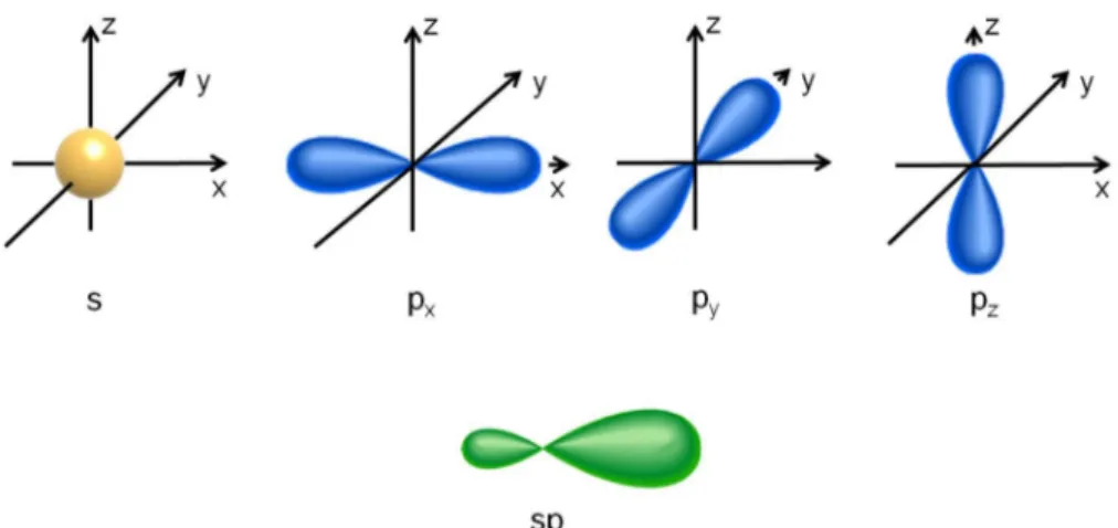
the combination of s and p ones. This process is called hybridization because it involves the merging of the spherical s orbital with the elongated p orbital to create new AOs (Figure 1.2). AOs are functions that describe the quantum states of electrons. The bigger lobe of the hybridized AO is the one which most probably contains the unpaired valence electron. Depending on how many orbitals are mixed, there will be different kind of hybridizations.
Figure 1.2: Representation of the spherical s, of the three elongated p and of the hybridized sp atomic orbitals.
1.1.1 sp3hybridization
The mixing of the s orbital with all the three p orbitals leads to the formation of four sp3 hybridized orbitals which arrange in a tetrahedral geometry to maximize the distance between the charges (Figure 1.3). Each sp3 orbital in fact contains one unpaired electron
and it is thus available for a covalent bond.
Figure 1.3: a) Representation of the tetragonal arrangement of four sp3 hybridized AOs; b) sketch of a single carbon-carbon bond.
1.1 Organic semiconductors 21
1.1.2 sp2hybridization
When the mixing includes the s orbital and two p orbitals, there is the formation of three sp2 hybridized orbitals, which arrange in a planar triangular geometry perpendicularly
crossed by the only left pure p orbital (Figure 1.4a). In a bond with another hybridized carbon atom, the head-to-head overlap between two sp2orbitals forms a σ bond, whereas the side-by-side overlap between two pure p orbitals forms a π bond (Figure 1.4b). The presence of a double bond connecting the carbon atoms arises from the constitution of these σ and π bonds (C=C).
Figure 1.4: a) Representation of the planar arrangement of three sp2hybridized AOs;
b) sketch of a double carbon-carbon bond.
1.1.3 sphybridization
If instead the s orbital is merged with only one p orbital there is the formation of two sp hybridized orbitals which arrange in a linear configuration; the other two pure p orbitals dispose perpendicularly with respect to each other and to the two sp AO.
Figure 1.5: a) Representation of the linear arrangement of two sp hybridized AOs; b) sketch of a triple carbon-carbon bond.
In a bond with another sp hybridized carbon atom, the head-to-head overlap between two sp orbitals forms a σ bond, whereas the side-by-side overlap between the two pure p orbitals forms two π bonds. These two π bonds together with the σ one are responsible for the triple bond between the adjacent carbon atoms (C≡C).
Organic semiconducting materials are π-conjugated materials, due to the presence of alternating single-multiple carbon-carbon bonds. This allows for the overlapping of p AOs and consequently to the delocalization of π electrons throughout the extended sys-tem. According to the molecular orbitals (MOs) theory, the wave function Ψ describing a valence electron in a molecule is characterized by quantum numbers depending on the form and energy of the AOs (ψ) involved. This Ψ can be approximated as a linear combination of AO (LCAO), resulting in:
Ψ =
n
cnψn (1.1)
If two atoms form a molecule, their AOs can combine in two ways:
Ψ = cAψA+ cBψB (1.2)
Ψ∗= cAψA− cBψB (1.3)
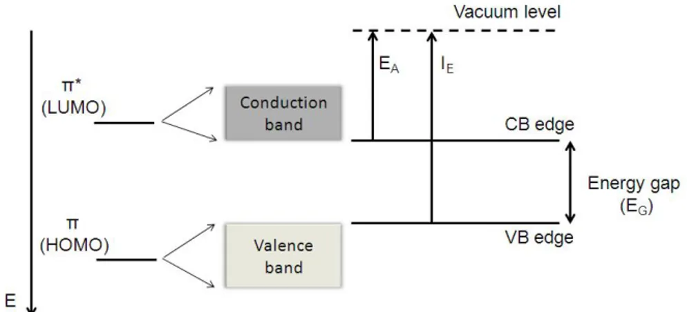
The molecular orbital resulting from the first case is called (π) bonding MO (or high-est occupied molecular orbital, HOMO), while the other one (π*) antibonding MO (or lowest unoccupied molecular orbital, LUMO). In general the number of MO is equal to the valence AOs. If the number of atoms forming the molecule increases, the HOMO and LUMO orbitals transform into valence and conduction bands containing the energy levels depending on the wave number k.
Figure 1.6: Band structure of an organic semiconductor deriving from the superpo-sition of many bonding and antibonding molecular orbitals.
In organic materials, the greater the number of conjugated π-bonds, the smaller the π-π* (i.e. HOMO-LUMO) energy difference is, in such a way that the absorption of electro-magnetic radiation in the UV-visible range or simply the thermal energy can promote electrons from the HOMO to the LUMO level.
1.1 Organic semiconductors 23
Organic semiconductors are mainly classified into two big classes: small molecules and polymers. Both classes comprise materials which show conduction of holes (p-type) and other which show conduction of electrons (n-type). Here just a brief list of the most com-mon small molecules and polymers is presented; more detailed information can be found in different reviews [1–6].
1.1.4 Small molecules
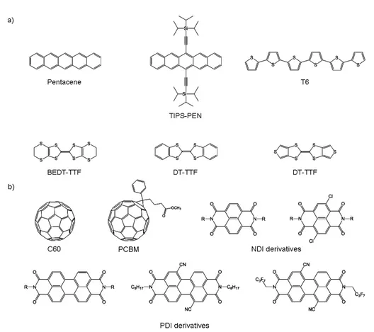
Organic small molecules are characterized by low molecular weight and are not prone to polymerization. They can easily be deposited via thermal evaporation, which ensures purification of the material at the expenses of cost and ease of processing, as well as from solution if properly functionalized. Due to their small size and fixed shape, they usually well organize on a surface and tend to form well-defined crystalline films. One of the most popular p-type small molecules in literature is pentacene, from the acenes family, that is composed by five benzene rings attached together. It strongly organizes in a herringbone structure forming polychristalline films with good holes mobility and stability but it is not soluble, so it can only be deposited by vacuum processes. To over-come the solubility issue, a functionalized pentacene (TIPS-PEN) has been synthesized by Anthony and co-workers [7] and mobilities up to 1 cm2/V swere obtained by Payne
and co-workers [8]. Other popular families of p-type organic small molecule for OFETs applications are the oligothiophenes [9, 10] and the tetrathiafulvalene (TTF) derivatives. Among oligothiophenes, sexithiophene (6T) is one of the most studied in literature [11]. TTF derivatives have been extensively studied by Rovira and co-workers [12, 13] and show a wide variety of applications as well as good electrical behaviour in OFETs. Ex-amples of the most performing n-type semiconducting molecules known in literature are fullerene (C60) [14, 15], and rylenes [16, 17] derivatives. The latter ones are polycyclic aro-matic electron-transport materials with high electron affinities and among these, many naphtalene and perylene diimides derivatives (respectively NDIs and PDIs) have shown high electron mobility as well as good thermal and photochemical stability. Moreover, the possibility of functionalization with cyano and alkyl groups makes these materials optimal for solution process depositions.
Figure 1.7: Examples of a) p-type and b) n-type small molecules.
1.1.5 Polymers
Conjugated polymers are composed of alternating single and double carbon bonds. Typ-ically, they are characterized by a rigid π-conjugated backbone, where the charges are de-localized, and flexible insulating side-chains. The backbone represents the main pathway for charge transport which is then defined as intra-chain transport, while the side-chains hinder the intermolecular attractions making the material soluble and highly process-able. Very often polymers organize on a surface in chains formed by repetitive units (or lamella) and the lamella of neighbouring chains can undergo partial π-orbitals over-lap thus favouring charge transfer from one chain to the other (inter-chain transport). Polymers are much unwieldy than small molecules and have difficulty in packing and rearranging; they tend to form relatively small crystalline domains with large population of defects. Their large polydispersivity, i.e. the size of the molecular weight distribution’s width, influences the formation of defects [18]. Poly(3-hexyl-thiophene) (P3HT) and poly(2,5-bis(3-alkylthiophen-2-yl)thieno[3,2-b]-Thiophene (PBTTT) are two of the most famous p-type polymers [19, 20]. Already in 1999 P3HT showed mobility values greater than 0.1 cm2/V s [21] and nowadays is employed for the fabrication and study of so-lar cells, and sensors [22]. Among the n-type polymers, poly[N,N’-bis(2-octyldodecyl)-naphtalene-1,4,5,8-bis(dicarboximide)-2,6-diyl]-alt-5,5’-(2,2’-bithiophene) (P(NDI2OD-T2))
1.1 Organic semiconductors 25
is up to date one of the most widely studied for electronic applications, due to its out-standing electrical properties related to an unconventional face-on molecular packing [23].
Figure 1.8: Examples of a) p-type and b) n-type organic plymers.
The predominance of publications regarding organic p-type materials is due to the ease of obtaining stable and performing devices based on p-type organics with respect to n-type ones. The main issues with n-type materials are: i) the big energy barrier between the electrode work function and the LUMO level of the molecule, ii) their high susceptibility to water and oxygen, iii) the electron trapping at the dielectric interface. To make tran-sistors that carry electrons the LUMO level of the molecules needs to match the electrode work function so that charge injection from the metal contact to the organic semiconduct-ing material becomes possible. The LUMO level must usually be lowered (i.e. the elec-tron affinity increased) to match the work function of the gold and this can be achieved by adding strong electron withdrawing groups like fluorines, cyanos or diimides to the
molecular core. The lowering of the LUMO also improves the air stability of the mate-rial by decreasing the trapping of charge carriers from H2O or O2. Another detrimental
mechanism of charge trapping is the one happening at the dielectric surface. The most common dielectric used is the thermally grown SiO2 which presents hydroxyl groups
(OH) on the surface; these groups act as traps for the electrons, so the passivation of the surface by means of self-assembled monolayers (SAM) is an obliged step.
1.2
Charge transport models
Due to the wide variety of small molecules and polymers available, many models have been proposed to describe charge transport in conjugated materials, but a lot of work has still to be done to formulate a complete and consistent theory. In this section, a brief review of the origin of charge transport in inorganic materials [24–26] is recalled before introducing the main theories developed for organic materials [27–30]. It is in fact impor-tant to note that the main difference on transport mechanisms between inorganics and organics arises from the presence or absence of long-range crystalline order.
1.2.1 Inorganic materials: nearly free-electron model
The nearly free-electron model is an evolution of the quantum free electron model, which describes the motion of electrons in a metal by combining the classical Drude theory of motion and the quantum Fermi-Dirac statistics. To predict the presence of forbidden bands, and thus find an explanation for inorganic isolating and semiconducting mate-rials, an important consideration has to be made: the electrons are nearly free, in the sense that they are slightly perturbed by the weak periodic potential deriving from the presence of atoms in the crystal lattice. The shape of the potential determines the exact solution of the Schr ¨oedinger equation for an electron in a crystal lattice, while the peri-odicity of the perturbation, i.e the presence of the lattice itself, gives the general shape of the nearly free-electron eigenfunction. This eigenfunction (Ψ) results in fact as a wave function whose amplitude is periodically modulated by the effective periodicity of the lattice
Ψ(x, t) = uk(x)ei(kx−ωt) (1.4)
with
uk(x) = uk(x + a) = uk(x + na) (1.5)
being a the the space periodicity of the lattice. Following the Kronig-Penney model, we can approximate the crystal potential in 1D (V (x)) as an array of rectangular potential wells and barriers reproducing the presence of the atoms. For wells that are close