Università degli Studi di Catania
Dottorato di Ricerca in Scienza dei Materiali
XXVI Ciclo
Gabriella Zappalà
Assembly and characterization of molecular
films for energetics and electronics.
Tutor: Prof. A. Licciardello
Coordinatore: Prof.ssa M. G. Grimaldi
Tesi di Dottorato di Ricerca
Dicembre 2013
“Learn from yesterday, live for today, hope for tomorrow.
The important thing is to not stop questioning”
1 Riassunto
Nell’ambito della ricerca scientifica, un crescente interesse viene rivolto all’ottenimento di dispositivi molecolari in grado di sostituire quelli macroscopici attualmente impiegati. Affinché ciò sia possibile è necessario uno studio approfondito dei fenomeni alla base dei processi di funzionamento dei diversi componenti e delle metodologie che possano permetterne l’assemblaggio. In questo contento si inserisce il presente lavoro di tesi di dottorato, il cui scopo è stato l’assemblaggio e la caratterizzazione di sistemi molecolari applicabili nell’ambito dell’elettronica e dell’energetica.
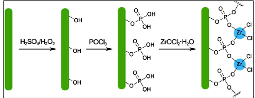
I sistemi studiati sono stati preparati seguendo un approccio bottom-up, ed in particolare è stato sfruttato il processo di self-assembling, che si basa sul chemisorbimento di molecole aventi funzionalità specifiche per la superficie considerata. Nel caso di superfici di oro sono state utilizzate molecole caratterizzate da un gruppo tiolico, mentre nel caso di superfici di ossidi si è scelto di applicare una metodologia sviluppata all’interno del nostro gruppo di ricerca, la metodologia dello zirconio fosfato-fosfonato (ZP) che sfrutta l’interazione di un gruppo fosfonico con gli ioni zirconio (precedentemente legati alla superficie), per cui sono state scelte molecole che aventi un gruppo fosfonico come gruppo attivo nei confronti della superficie.
La prima parte del lavoro è stata dedicata alla preparazione e caratterizzazione di fili molecolari a base di complessi politerpiridinici del ferro ancorati su substrati di oro. Essi sono stati ottenuti sfruttando un processo iterativo che coinvolge una serie di reazioni di complessazione tra un metallo (nel caso specifico FeII) e un legante contenente una doppia funzionalità terpiridinica. È stata condotta una caratterizzazione sia chimica, mediante spettroscopia di fotoelettroni (XPS) e spettrometria di massa di ioni secondari con analizzatore a tempo di volo (ToF-SIMS), sia strutturale tramite spettroscopia near edge
X-ray absorption fine structure (NEXAFS). L’attenzione è stata poi in particolare
rivolta allo studio delle proprietà di conduzione molecolare di tali sistemi mediante microscopia a forza atomica con punta conduttiva (conductive atomic
2 La seconda parte del lavoro è stata focalizzata sullo sviluppo di metodologie utili per la funzionalizzazione di substrati di ossidi utilizzabili nell’ambito dell’energetica molecolare. Come detto, la funzionalizzazione di tali substrati è stata ottenuta applicando la metodologia “ZP”. Sono stati condotti studi riguardanti il ricoprimento e la stabilità dei monostrati ancorati, sfruttando un derivato fosfonato della rodamina B. Quindi tale metodologia è stata estesa a substrati di TiO2 (nella forma di anatasio), in quanto esso è attualmente il substrato maggiormente utilizzato nella costruzione di celle fotoelettrochimiche. Sono state preparate diverse tipologie di film su tali superfici, e –tra l’altro - è stata verificata la possibilità di formare un bistrato auto assemblato formato da un complesso dendrimerico del Ru(II), che funge da sensibilizzatore, e da un poliossometallato capace di fungere da catalizzatore per lo splitting foto indotto dell’acqua. I diversi campioni sono stati caratterizzati tramite indagine ToF-SIMS e UV-visibile.
Infine è stato affrontato il problema generale dell’ottenimento di profili di profondità molecolari di sistemi polimerici. Al fine di studiare l'applicabilità del metodo su sistemi multistrato a base polimerica, sono stati preparati multistrati polielettrolitici mediante deposizione layer- by-layer. Tali campioni sono stati caratterizzati tramite cluster-SIMS dinamico in modalità dual beam e sono stati studiati gli effetti della natura e dello spessore degli strati polimerici sull’ottenimento di profili di profondità molecolari. I profili di profondità di questi sistemi ottenuti hanno evidenziato che la possibilità di ottenere un buon profilo dipende dall'ordine in cui sono depositati gli strati contenenti polimeri aventi un comportamento radiochimico diverso. In particolare , si è scoperto che la presenza di uno strato che tende ad accumulare “danno da radiazione” ha un effetto negativo anche sulla profilabilità degli strati sottostanti. Tale problema può essere superato introducendo un radical scavenger (ossido nitrico) nella camera di analisi durante l’acquisizione dei profili di profondità. Nell’ambito di tale ricerca il cluster-SIMS è stato applicato allo studio di sistemi di interesse nel campo dell'elettronica molecolare. In particolare, è stato possibile evidenziare, dai profili di profondità ottenuti, fenomeni di separazione di fase lungo la profondità in in sistemi costituiti da miscele binarie di oligotiofeni.
3
Table of contents
Introduction... 5
1 Nanoscale electrical investigation molecular wires ... 9
1.1 Molecular electronics ... 9
1.1.1 Molecular junction ... 10
1.1.2 Self assembling ... 11
1.1.3 Charge transport mechanism ... 14
1.1.4 Conductive-AFM ... 16
1.1.5 Supramolecular wires. ... 18
1.2 Results and discussion ... 20
1.2.1 ToF SIMS characterization ... 21
1.2.2 UV-Vis characterization ... 22 1.2.3 XPS analysis ... 22 1.2.4 NEXAFS analysis ... 26 1.2.5 C-AFM measurements ... 28 1.2.6 Theoretical calculations ... 37 1.3 Conclusions ... 39 1.4 References ... 39
2 Oxide surface engineering ... 47
2.1 Solar energy conversion: the molecular approach. ... 47
2.1.1 Water splitting dye sensitized solar cells ... 48
2.1.2 Self assembling on oxide substrates ... 55
4 2.2.1 Zirconium phosphate-phosphonate anchoring (ZP method) on on
quartz surfaces. ... 61
2.2.2 TiO2 functionalization ... 67
2.2.3 Thermal stability of the layers anchored on TiO2 via ZP procedure ... 70
2.2.4 Self assembly of a sensitizer/catalyst bi-layer for photo-induced water splitting ... 76
2.3 Conclusions ... 80
2.4 References ... 81
3 Molecular depth profiling of organics and polymers ... 87
3.1 Cluster SIMS ... 89
3.2 Polyelectrolyte multilayers as model systems for molecular depth profiling. ... 100
3.2.1 Polyelectrolyte multilayers preparation ... 102
3.2.2 SIMS Molecular depth profiling ... 107
3.3 Molecular depth profiling of oligothiophenes ... 114
3.4 Conclusions ... 117
3.5 References ... 118
4 Conclusions ... 123
5
Introduction
The problematics related with the current trends in miniaturization of techonological devices and the consequent search for suitable materials and methods have, since some years, an important impact in materials science. The transition from “micro” to “nano” materials offers several advantages. One of them is the increase of surface area, with the consequence that typical bulk properties become governed by surface properties. Products of micro- and nano-technology provide several advantages over conventional macroscopic structures, including lower power consumption, higher efficiency, and many others interesting features that are depending on the properties of materials at the micro- and nanometer scale. Nanotechnology is the engineering of functional systems at the molecular scale in order to develop precise machine and components with sizes comparable with the molecular ones (0.1-100nm). Research in nanotechnology and in nanoscience has given very promising results also in terms of industrial and commercial applications in many areas, including – among others - energy production, storage and conversion, production of new materials, health-related applications and information technology. A branch of nanoscience and nanotechnology is dedicated to the obtaining of molecular devices, which can be defined as chemical systems structurally organized and functionally integrated, consisting of the union of different molecular components having different properties.
In order to obtain nanodevices the classical top down approach (typical, for example, of many microelectronics-related technologies), needs to be replaced, or at least integrated, with a bottom up approach in order to fabricate nanostructures with well controlled properties, such as molecular machines for specific applications.
The way for the bottom-up approach is based on chemistry, either “conventional” or supramolecular. In particular it is possible to form self assembled structures thanks to “the spontaneous association of molecules
6 under equilibrium conditions into stable, structurally well-defined aggregates joined by non-covalent bonds”[1].
In this respect, part of research is focused on the development of new molecular building blocks that can improve the efficiency and the stability of the built nanomachine and on to the development of the suitable assembling methods. In this context supramolecular chemistry plays an important role because it allows to form supramolecular entities, “supramolecules”, which possess new properties, thanks to the combination of molecular chemistry with non-covalent interactions. The properties of the supramolecular entities are not necessarily the sum of the properties of the individual assembled molecules. In fact, the widely accepted definition of supramolecular chemistry was given by Jean -Marie Lehn: "Supramolecular chemistry is the chemistry of the intermolecular bond, covering the structures and functions of the entities formed by the association of two or more chemical species."[2]
As mentioned above, realization of nanostructured devices using the bottom-up approach is required in nanotechnology, and supramolecular chemistry allows building of functional materials starting from molecular components that self-assemble via chemical bonds, using the principles of molecular recognition. Moreover the fabrication of devices through the bottom-up approach generally needs to integrate the supramolecular system in a solid device, which doesn’t act as a simple support, but generally plays an active role in the device (for example as electrode in an electronic device). In this context the role of the surface becomes important in order to obtain a good control of the system properties, so that it is necessary not only to develop methods for the preparation and modification of molecular and supramolecular surfaces, but also to develop suitable characterization techniques allowing a fine monitoring of surface properties, including chemical composition, morphology and structure.
Many methods have been employed for surface engineering, and in particular some of them are based on the modification of existing layer, while others rely on addition of new layers onto the surface by formation of molecular thin films. According to the kind of system to be prepared, it is possible to use
7 different techniques, including, among others, spin coating, [3] Langmuir-Blogdett deposition,[4] self assembly. [5]
For the to the characterization of thin films and surfaces, several techniques are available. Among them, scanning probe techniques, and in particular Atomic Force Microscopy, are very useful since they allow a precise study of the morphology of the surface, in a nanoscale dimension, as the lateral resolution is typically of the order of 20 nm (and in some special cases it can be pushed down to atomic resolution) while the vertical resolution can be of the order of 0.1 nm. Nevertheless, AFM doesn’t give significant amount of chemical information, although some information in this direction can be sometimes obtained. For this reason, morphological studies have to be coupled with other techniques able to provide extensive chemical information. Among them, time-of-flight secondary ions mass spectrometry (ToF-SIMS) allows chemical characterization of the surface with very high sensitivity and good lateral resolution, allowing not only the detection and three dimensional mapping of all the elements, including hydrogen, but also providing a large amount of molecular information on the species present at the surface and, with some limitations, along the depth of molecular films.
The present thesis work is focused on the preparation and characterization of functional thin films for energetics and molecular electronics. In this framework, some preparation methods have been developed, and the systems of interest have been studied by using different techniques such as time-of-flight secondary ion mass spectrometry (ToF-SIMS), conductive atomic force microscopy (C-AFM) and UV-visible spectroscopy. The thesis is divided in three main sections.
Chapter 1 deals with self-assembled supramolecular wires of interest for molecular electronics. They have been prepared and characterized both from the compositional/structural point of view and from the point of view of their electrical properties. For the latter purpose, conductive-AFM measurements were carried out in order to understand the electrical characteristics at the nanometre scale and the underlying electron transport mechanisms.
The second chapter deals with a method for functionalizing oxide surfaces, and in particular TiO2 surfaces, suitable for building-up dye sensitized electrodes
8 exploitable in solar energy conversion applications. In particular, a stable way of dye anchoring has been demonstrated for such surfaces, and it has been applied to the preparation of surface-anchored monolayers of different kind of molecular and supramolecular dyes. Also, the method has been employed for the formation of a molecular bilayer that could be applied in photoinduced water splitting devices.
Chapter 3 is dedicated to the problem of in-depth characterization of molecular layers, which is an open topic of large interest in many technological fields, including molecular electronics and organic-based energy conversion devices. In particular, a SIMS method (NO-assisted cluster-SIMS) has been studied, that gives promising results in this direction. With the aim of studying the applicability of the method to polymer-based multilayers, well-controlled layered systems have been prepared by means of layer-by-layer polyelectrolyte deposition. Moreover, the cluster SIMS technique was used in the study of in-depth phase separation oligothiophene based blends.
Finally, in order to make more fluid the presentation and discussion or the results, many experimental details were described in a dedicated Appendix section.
References
[1] Whitesides, G.M., Mathias J.P., Seto C.T., Science. 1991, 254, 1312-1319. [2] Jean- Marie Lehn , Supramolecular chemistry- scope and perspectives
molecules-supermolecules- molecular devices. Nobel lecture, December 8, 1987
[3] D. W. Schubert, Polym. Bull., 1997, 38, 177-184 [4] I.R. Peterson, J. Phys. D , 1990, 23, 379–95
9
1 Nanoscale electrical investigation molecular wires
1.1 Molecular electronics
According to Moore’s law the number of transistors per square centimetre of silicon doubles every 18 months.[1] Miniaturization of silicon-based structures has several limits that make this law impractical. In particular the limitation is due to the top-down approach used to miniaturize the electronic components, that is the use of techniques such as electron beam lithography and micro-contact printing, in which the lateral dimension that can be obtained is in the order of hundred nanometres. By contrast, a top-down approach can be used, starting from molecular building blocks to form self-assembled structures with a nanometric dimension.
It is clear since several years that molecular electronics can be a valid alternative to the silicon technology, and to reach this goal not only is necessary to use molecules with exceptional electronic properties, but also to integrate them into an appropriate electronic circuit with an efficient method. Already in 1959 the eminent physicist Richard Feynman opened the discussion of obtaining extremely small devices in his lecture entitled “There’s plenty of room at the bottom”.[2] Scientific knowledge was not adequate at the time, but thanks to the progresses achieved in the ‘90s, it is now a fact that a large community of scientists is working on the use of single molecules as electronic components.
In a single-molecule electronic device electrodes must be connected by a system indicated as a “conductive molecular wire”, that is a molecular system able to transfer a signal transferring excitation energy, or moving holes or electrons. The use of organic molecular wire offers many advantages; the first is the high level of control of the structural and electronic properties that can be easily obtained. Moreover, several conjugated molecules can be built so that they can self-assemble into supra-molecular structures suitable for charge transport [3] and thereby they can possibly be exploited to assemble molecular wires into electronic circuits. In this context supramolecular interactions play
10 an important rule and it has already been shown that they can be used to control the optical and charge transport properties of conjugated molecular wires. [4-6]
One of the first study in single-molecule conduction was made by Gimzewski and Joachim who measured the electrical conductance of a single fullerene C60 molecule. [7] Other pioneer experiments were carried out by Reed et al.,[8] who measure the electrical resistance of a single benzenedithiol molecule, and by Metzger et al.,[9] who demonstrated the single-molecule rectification. Since these early studies, a high level of knowledge has been achieved in molecular electronics, both in the practical problem of building single molecules device and characterizing them and in the fundamental understanding of the electrical mechanisms involved.
1.1.1 Molecular junction
In the context of the emergence of molecular electronics, the study of charge transport through molecular wires has become an important research topic. In order to obtain information about molecular conduction it is necessary to construct a molecular junction, i.e. a system in which two metal electrodes are connected with molecules. In a so built device, the conductivity is simply determined by measuring the current-voltage (I-V) characteristics.
11 Molecular junctions can be formed using several methods, [11-15] that allow to form them in a reproducible way, and to enable studies of conduction properties as a function of molecular length [16-18] applied voltage,[19] temperature,[20-21] ecc…
The most difficult step in the construction of a molecular junction is the application of the second electrode, and several methods have been developed, including the evaporation of a metallic counter-electrode onto the organic film, mechanical break junction,[22-23] mercury drop measurements,[24-25] scanning probe microscopy (SPM), including conducive atomic force microscopy (C-AFM). [26-30]
1.1.2 Self assembling
The most common strategy to form a molecular film on a substrate is the self-assembling technique, which is the spontaneous formation of complex structures from molecular building blocks. Self-assembled monolayers, SAMs, are molecular aggregates that form when surfactant molecules spontaneously adsorb on surfaces. Molecules suitable to form SAMs should have a chemical functionality, the “head group”, able to react chemically with the substrate and a second one, the “tail group”, which is conveniently chosen in order to give a new functionality to the surface. The “backbone” of the molecule (or “spacer”), connects tail and head groups and generally provides stability to the self-assembled film thanks to the interactions with the backbones of the other molecules. (Figure 2).
12
Figure 2. Schematic diagram of an SAM on a substrate.
SAMs are generally easy to prepare, they do not require specialized equipment in their preparation and they can form nanometre-scale objects (for example, thin films, nanowires, nanodomains, and other nanostructures). Moreover, by modifying the “tail group” of the surfactant, surface properties can be easily tuned. For these reasons SAMs can be considered as ideal model systems in many fields. [31-33]
Alkanethiols on metals are the most extensively studied class of SAMs.[34-41] The high affinity of thiols for the surfaces of noble and coinage metals makes possible to generate well-defined organic surfaces (Figure 3) with useful chemical functionalities at the exposed interface.[42]
13
Figure 3. Formation of well-defined SAM film on gold surface. [35]
The most common protocol for preparing SAMs on gold and other materials is by immersion of a freshly prepared or clean substrate into a diluted (millimolar) solution of thiols in ethanol for ~12-18 h at room temperature. This procedure resulted from a combination of studies planned to optimize the reproducibility of the SAMs.[43] It is possible to obtain dense coverage of adsorbates quickly (milliseconds to minutes) from millimolar solutions, but, in order to maximize the density of molecules and minimize the defects in the SAM, a slow reorganization process is required (hours). A very wide number of experimental factors can affect the structure of the resulting SAM and the rate of its formation, such as solvent, temperature, adsorbate concentration, immersion time, purity of the adsorbate, concentration of oxygen in solution, cleanliness of the substrate, and structure of the adsorbate itself.[44]
Thiol monolayers comprising a well-defined mixture of molecular structures are called “mixed” SAMs. There are different methods for synthesizing mixed SAMs, the most common being coadsorption from solutions containing mixtures of thiols and adsorption of asymmetric disulphides or asymmetric dialkylsulfides. Mixed SAMs provide a useful methodology for incorporating
14 into a SAM a molecular species that for some reason (steric hindrance, presence of charges) cannot form directly a well-organized assembly.
1.1.3 Charge transport mechanism
The charge transport mechanism of a molecular wire can be understood looking at the dependence between its electrical resistance and its length. It is well known that, if the wire is short enough, electrons can tunnel between the two electrodes; while in the case of longer wires electrons are transported thanks to a hopping mechanism.
If a tunnelling mechanism occurs, electrons traverse a potential barrier and propagate on the other side without changing their phase. The tunneling mechanism is often ‘‘non-resonant’’ in that the tunnelling electron energies are not precisely matched with the molecular orbital energies; however, the frontier molecular orbitals still assist the tunnelling process (i.e., they lower the junction resistance) by lowering the effective tunnelling barrier[45].
Figure 4. Transmission of electron wavefunction thtough a potential barrier. [10]
For this kind of mechanism, resistance R is connected to the wire length L by the equation:
R=R0 exp(βL)
where R0 is the effective contact resistance and β is a structure dependent attenuation factor. According to this equation, it is possible to find the value of
15 R0 and β from a semi log plot of R versus molecular length. Efficient tunnelling is characterized by low values of β, in the range of 2.0-5.0 nm-1 in the case of delocalized π electrons and between 7.0 and 10.0 nm-1 in the case of a saturated chain. R0 is depending by the type of metal and the kind of connection between surface and molecules.
In conjugated molecular wires longer then few nanometres tunnelling mechanism cannot occur; the charge conduction occurs through a serie of discrete steps, involving a initial charge injection in the molecular orbitals of wire, the field-induced drift of the charge carrier down the length of the molecule, and finally the extraction of the charge into the receiving contact.
Figure 5. Schematic energy diagram for incoherent hopping through N sites [10]
The hopping mechanism is thermally activated and can be described using an equation that follows a classical Arrhenius behaviour:
R=R0 exp(Ea/kT)
In which Ea is an activation energy and k is the Boltzmann constant. In tunnelling regime, as said before, there is an exponential dependence between R and molecular length; in case of hopping mechanism on the contrary there is a linear correlation in the low bias regime, and this different behaviour allows a charge transport over longer distances.
16 From the above it is clear that electron conduction mechanism depends on several factors including electronic structure, molecular length, temperature, applied bias. For these reasons, a deep understanding of the electrical behaviour of a molecular junction involves both experimental and theoretical studies.
There are several examples reported in recent years. Selzer et al [46-47] studied the thermal dependence of the electrical behaviour in nitro-substituted oligo-phenylene-ethylene (OPE), and they show that there is a transition from a independent behaviour at low temperature to a temperature-dependent behaviour at high temperature, that is a transition from a tunnelling mechanism to a hopping one.
More recently, Frisbie et al. [20] published a study on oligophenyleneimine (OPI) in which the electrical behaviour of molecular wires with different length was studied by using conductive AFM. They show that for short wires there is a tunnelling transport mechanism, and that there is a transition to a hopping mechanism for wires longer than 4 nm, as supported by the dependence of electrical characteristics as function of length, temperature, and electric field.
1.1.4 Conductive-AFM
Conductive probe atomic force microscopy is a variant of the “classical” atomic force microscopy, in which a tip with a conductive coating is used as second electrode. This tip is brought into contact with surface with a known applied force. In order to measure I-V characteristics a voltage between the sample and the tip is applied and the resulting current is measured. The resistance is calculated from the inverse of the slope of the I-V obtained curve at small voltages, where the correlation is generally linear.
17
Figure 6. Schematic rapresentation of a set up for conductive AFM.
Two configuration can be used, the horizontal one and the vertical one. The first one allows measuring the current between the AFM tip and a metallic contact on insulating substrate. The second one is used with conductive substrates and it is well suited for studying the electrical properties of ultrathin films, such as self-assembled monolayers. (Figure 7)
Figure 7. Schematic representation of the arrangement used for C-AFM measurements in vertical configuration (left) and in horizontal configuration (right). [26]
C-AFM is useful also for imaging: by applying a constant voltage between the tip and the substrate and by scanning the surface, it is possible to record the current as a function of the position of the tip, so obtaining a map of the local sample conductivity.
18 1.1.5 Supramolecular wires.
Supramolecular chemistry can be very useful in obtaining a wide range of system with different properties. In this particular context, polymetallic (supramolecular) complexes can be used as models for the study of electron transport mechanism in a molecular junction. Generally, supramolacular polymers can be obtained from the complexation of metal ions and ditopic ligands. Although the toxicity of some metals can be seen as a drawback, this strategy for obtaining molecular wires has several advantages, such as the high specificity and directionality (provided that suitable ligands are choosen).
Figure 8. Schematic representation of the metallo-supramolecular polymerization process.
With the aim of building functional complexes, that show luminescence, and/or have interesting electrochemical properties, or display photoinduced energy- and electron-transfer processes, the choice of suitable bridging ligands is crucial. In fact, according to their coordinating sites, they contribute to determine the spectroscopic and redox properties of the active metal-based units; moreover, their chemical nature controls the electronic communication between the metal-based units. As a consequence the choice of appropriate building blocks makes possible to tailor the supramolecular polymer properties by combining the characteristic features of a metal ligand complex (such as
19 electrochemical, optical, magnetic properties) to the ones of polymers (processability, mechanical properties, solubility, etc..).
Among many ligands, terpyridine derivatives are widely used as building blocks in supramolecular and macromolecular chemistry. In particular 2,2':6',2''-terpyridines derivatives (tpy) are tridentate ligands which can complex a variety of transition metal ions with a high binding constant, forming structures with very interesting optical, magnetic and electrochemical properties. [48]
Figure 9. Example of terpyridine-based metal complex.
To understand the photophysical properties of these compounds many studies have been made by looking at the photo-induced electron transfer reactivity, [49-51] in order to extend their use in optoelectronic devices, e.g. as dye sensitizers [52] Their application in electronics has been hampered by a relative lack of knowledge on their charge transport behavior in the solid state. For this reason several electrochemical studies were made in order to explore the redox conduction properties of polymers bearing terpyridine complexes in the side chains. [53-54] Since the structural versatility of the coordination compounds allows for the fabrication of well-defined architectures, such as quasi-1D structures, they are also being considered as possible building blocks for the fabrication of conductive molecular wires.[55-56] Stepwise coordination reactions involving terpyridine functions have been successfully exploited to connect the molecular wires to solid surfaces as gold, [57-58] silicon,[59] and oxides,[60-61] and to lengthen the wires up to tens of nanometers. [62-65]
20
1.2 Results and discussion
In order to prepare ordered molecular wires using a bottom-up approach, it is first necessary to form a stable platform on the substrate. It is well known that using a system made by a mixture of a terpyridine derivative (4-[2,2':6',2''-terpyridin]-4'-yl-benzenethiol, MPTP) and benzenthiol (MB), it is possible to obtain a well ordered monolayer on gold. In such a film, in which the MPTP acts as the functional component and the MB as a lateral spacer, the two components are perfectly interconnected, due to the strong lateral interaction between the MB and the head group side of the MPTP. [66-67]
Starting from this kind of platform, molecular wires can be constructed exploiting the affinity of terpyridine with transition metals and using a bifunctional terpyridine ligand, such as the 4’,4’’’’-(1,4-phenylene)bis(2,2’:6’,2’-terpyridine) (TPT).
To prepare the self-assembled platform, Au(111) substrates were incubated in a mixed solution of MB and MPTP in a 1:1 ratio. After rinsing, the stepwise construction of the molecular layers was carried out by dipping Au-MB/MPTP sample in (i) a solution of Fe(II) salt and then in (ii) a solution of TPT ligand. Steps (i) and (ii) were repeated iteratively in order to grow multilayers, and each iteration represents a coordination step, adding one Fe-TPT unit to the molecular nanowire.[62]
21 In the following samples will be indicated as nFeTPT, where n is the nominal number of complex layers, i.e. the number of preparative coordination steps. 1.2.1 ToF SIMS characterization
Time-of-Flight Secondary ion Mass Spectrometry (ToF SIMS) measurements were carried out in order to verify the success of each step of reaction. Indeed the technique gives information on the uppermost surface layers, with high sensitivity, high mass resolution and, in static mode, with very low surface damage. This makes ToF-SIMS well suited for providing molecular information from surfaces, even those – such as molecular ones – that are very sensitive to the damage induced by the ion beam acting as a probe in SIMS .
Figure 11 shows a typical spectrum obtained for samples after the formation of the first layer MPTP-Fe-TPT. It is possible to observe some characteristic fragments, including the quasi-molecular ion at 936 Da (C57H38N9SFe+), the MPTP and TPT protonated ions (C21H14N3S at 341 Da and C36H24N6 at 541 Da, respectively), the MPTP-Fe ion (396 Da) and the TPT-Fe ion (596 Da). This is an evidence that using this approach it is possible to
form bisterpyridine-Fe complex, and consequently to grow multilayers.
Intensit y (c ounts ) C21H14N3SFe+ C36H24N6Fe+ C57H38N9SFe+ C21H14N3SAu+ C21H14N3SH+ C36H24N6+ m/z, Da
22 1.2.2 UV-Vis characterization
Tof-SIMS measurements provide a qualitative information about the formation of the complex at the surface, but in order to verify the multilayer growth and to have a quantitative estimation of it, it is necessary to use other techniques. For that purpose multilayers were grown on semitransparent gold substrates (evaporated on quartz) in order to monitor changes in surface plasmon band of gold using UV-Visible measurements, since this is strongly sensitive to the thickness of adsorbed molecular layers.[68-69]
600 800 1000 1200 0,2 0,3 0,4 0,5 0,6 0,7 0,8 A bs nm SAM 2FeDT 3FeDT 4FeDT 0 1 2 3 4 850 900 950 1000 1050 1100 ma x ( nm) # layer
Figure 12. a) gold plasmon band of nFeTPT layers; b) gold plasmon band maximum as a function of number of layers.
Figure 12 shows clearly that the maximum of the band related to the plasmon moves linearly toward higher wavelengths with the increasing of the number of layers, as expected from literature, and this is an evidence of the success of the multilayers growth.
1.2.3 XPS analysis
In order to increase the chemical information about the surface and to get additional information on the multilayer growth, X-Ray photoelectron spectroscopy (XPS) measurements with synchrotron radiation were carried out for MB-MPTP monolayer and for each nFeTPT layer. Such measurements
23 were done by in collaboration with Prof. Michael Zharnikov’s group (Angewandte Physikalische Chemie, Universität Heidelberg).
Figure 13a shows the Au 4f7/2 XP spectra acquired at a photon energy of 580 eV; it is possible to observe that the intensity of the substrate signal decreases upon the successive addition of the TPT units due to the increasing attenuation of the photoelectron signal by the growing overlayer. This trend confirms the linear growth of iron-based multilayers.
Looking at the C 1s XP spectra, Figure 13b, (acquired at a photon energy of 350 eV) and at N 1s XP spectra, Figure 14a, (acquired at a photon energy of 580 eV), it is also possible to observe that nFeTPT films exhibit only one emission at a BE of 285.0-285.1 eV related to the carbon atoms in the TPT units, and only one emission at a BE of ~399.7 eV related to the nitrogen atoms in the terpyridine moieties. [70-71] In both cases the signal is saturated because of the strong self-attenuation; therefore there are no intensity differences between the spectra. The spectrum of the MB/MPTP template differs a little bit from the other spectra because of the contribution of the MB molecules and effect of the substrate.
24
Figure 13. a) Au 4f7/2 XP spectra of the MB/MPTP and nFeTPT films acquired at a photon energy of 580 eV; b) C 1s XP spectra of the MB/MPTP and nFeTPT films were
acquired at a photon energy of 350 eV
292 290 288 286 284 282 280 5FeTPT/Au 4FeTPT/Au 3FeTPT/Au 2FeTPT/Au MB/MPTP/Au 1FeTPT/Au In te n s ity (a rb . u n its )
Binding energy (eV) C 1s h = 350 eV 86 85 84 83 82 81 80 5FeTPT/Au 4FeTPT/Au 3FeTPT/Au 2FeTPT/Au MB/MPTP/Au 1FeTPT/Au In te n s ity (a rb . u n its )
Binding energy (eV)
Au 4f h = 580 eV
25
Figure 14. a) N 1s XP spectra of the MB/MPTP and nFeTPT films were acquired at a photon energy of 580 eV; b) Fe 3p XP spectra of the MB/MPTP and nFeTPT films were
acquired at a photon energy of 580 eV
From the Fe 3p XP spectra shown in Figure 14b (acquired at a photon energy of 580 eV) it is possible to observe that nFeTPT films exhibit pronounced Fe 3p3/2,1/2 doublet at a BE of ~56.0 eV assigned to the bridging Fe atoms. The signal is saturated because of the strong self-attenuation; therefore, there are no intensity differences between the spectra. As expected, due to the small thickness of the organic layer, the spectrum of the MB/MPTP template exhibits a Au 5p1/2 emission at ~57.4 eV,[72] in the same region of the Fe 3p band.
404 402 400 398 396 394 In te n s ity (a rb . u n its )
Binding energy (eV) N1s h = 580 eV 5FeTPT/Au 4FeTPT/Au 3FeTPT/Au 2FeTPT/Au 1FeTPT/Au MB/MPTP/Au 65 60 55 50 In te n s ity (a rb . u n its )
Binding energy (eV) Fe 3p h = 350 eV 5FeTPT/Au 4FeTPT/Au 3FeTPT/Au 2FeTPT/Au 1FeTPT/Au MB/MPTP/Au a) b) c) d)
26 1.2.4 NEXAFS analysis
In order to obtain structural information of the MB/MPTP and nFeTPT films, NEXAFS investigation has been carried out, again in collaboration with Prof. Michael Zharnikov.
Figure 15. a) C K-edge NEXAFS spectra of the MB/MPTP and nFeTPT films acquired at an X-ray incidence angle of 55°; b) Difference between the C K-edge spectra of the MB/MPTP and nFeTPT films collected at normal (90°) and grazing (20°) angles of X-ray
incidence for the above samples.
Figure 15a shows the C K-edge NEXAFS spectra of the MB/MPTP and
nFeTPT films acquired at an X-ray incidence angle of 55°. The spectra of the nFeTPT films exhibit the characteristic double peak due to the C 1s→*
transition of the pyridine ring carbon at 285.0 eV (1) and 285.5 eV (2),
280 290 300 310 320 2 1 4FeTPT/Au 5FeTPT/Au 3FeTPT/Au 2FeTPT/Au 1FeTPT/Au 55° C K-edge Intens it y ( arbi trar y uni ts)
Photon energy (eV) MB/MPTP/Au 280 290 300 310 320 90°-20° C K-edge Intens it y ( arbi trar y uni ts)
Photon energy (eV) 1FeTPT/Au MB/MPTP/Au 3FeTPT/Au 2FeTPT/Au 5FeTPT/Au 4FeTPT/Au a b
27 observed also for pyridine-substituted self-assembled monolayers. The weight of the resonance 1 is larger in the spectrum of the MB/MPTP template since it overlaps with the * resonance from the MB moieties. In order to evidence the features associated with angular dependence, it is shown (Figure 154b) the difference between the C K-edge spectra of the MB/MPTP and nFeTPT films collected at normal (90°) and grazing (20°) angles of X-ray incidence for the above samples. This difference is representative of the linear dichroism in X-ray absorption, and the positive peaks at the positions of the resonances 1 and 2 suggest predominant upright orientation of the MPTP and MB moieties in the case of the MB/MPTP template and nFeTPT chains in the case of the
nFeTPT films. The difference peaks are especially strong in the spectrum of
the MB/MPTP template due to the contribution of the BT moieties, which seem to have pronounced upright orientation.
The N K-edge NEXAFS spectra of the MB/MPTP and nFeTPT films acquired at an X-ray incidence angle of 55° are reported in Figure 16. The spectra of the
nFeTPT films exhibit the characteristic *-like resonances of terpyridine at
398.7.0 eV, and the difference between the C K-edge spectra of the MB/MPTP and nFeTPT films collected at normal (90°) and grazing (20°) angles of X-ray incidence for the above samples and the positive peaks at the positions of the absorption resonance at 398.7.0 eV suggest predominant upright orientation of the MPTP moieties in the case of the MB/MPTP template and the nFeTPT chains in the case of the nFeTPT films.
28
Figure 16. a) N K-edge NEXAFS spectra of the MB/MPTP and nFeTPT films acquired at an X-ray incidence angle of 55°; Difference between the C K-edge spectra of the MB/MPTP and nFeTPT films collected at normal (90°) and grazing (20°) angles of X-ray
incidence for the above samples.
1.2.5 C-AFM measurements
The data reported above demonstrate the ability of building, on gold substrates, well ordered and contamination free self assembled FeTPT multilayers, that can be regarded as an assembly of molecular wires with upright orientation with respect to the surface plane. Electrical properties of this kind of systems have already been investigated by using the macroscopic mercury-drop technique.Errore. Il segnalibro non è definito. Here we focused our attention on the study of the nanoscale charge transport mechanism across the wires by using the
400 410 420 430 5FeTPT/Au 4FeTPT/Au 3FeTPT/Au 2FeTPT/Au 1FeTPT/Au 55° N K-edge Intens it y ( arbi trar y uni ts)
Photon energy (eV) MB/MPTP/Au 400 410 420 430 90°-20° N K-edge Intens it y ( arbi trar y uni ts)
Photon energy (eV) 1FeTPT/Au MB/MPTP/Au 3FeTPT/Au 2FeTPT/Au 5FeTPT/Au 4FeTPT/Au a b
29 Conductive Atomic Force Microscopy. Measurements were performed at Institut de Science et d'Ingénierie Supramoléculaires (ISIS), Stasbourg, in collaboration with the group of Prof. Paolo Samorì, during some stage periods. C-AFM measurements were carried out using a Digital Instruments Dimension 3100 AFM with a Nanoscope IV controller, using Pt/Ir coated silicon cantilevers with a nominal spring costant of 0.2 N/m. Measurements were acquired in contact mode and one hundred junction were established on each molecular layer. The I-V current-voltage data were first treated by discarding both the zero-current plots (see example of Figure 17a) and the saturated ones (Figure 17b), being originated from bad contacts or by direct contact of the C-AFM tip with the gold substrate, respectively . The statistics of the I-V measurements are reported in Table 1.
-1,0 -0,5 0,0 0,5 1,0 -10 -5 0 5 10 nA V -1,0 -0,5 0,0 0,5 1,0 -1,0 -0,8 -0,6 -0,4 -0,2 0,0 0,2 0,4 0,6 0,8 1,0 nA V
30 n of junctions n of good junctions % of working junctions MB-MPTP 111 48 43 1 FeTPT 139 65 47 2 FeTPT 100 53 53 3 FeTPT 210 56 27 4 FeTPT 91 30 33
Table 1. Statistical evaluation of the current-voltage measurements.
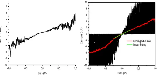
The further treatment of the “good” experimental I-V data is illustrated in Figure 18 in the case of MB/MPTP sample. The procedure is performed as follows: working curves are averaged (red curve ) and a linear fitting of this curve in low bias regime is obtained (green line), with the aim of obtaining information about the resistance value.
Figure 18. A typical working I-V (on the left); all the working curves obtained for a sample (in black), the average curve (in red) and its linear fit in the low bias region (in
green) (on the right).
-1,0 -0,5 0,0 0,5 1,0 -10 -8 -6 -4 -2 0 2 4 6 8 10 C u rre n t (nA ) Bias (V) -1,0 -0,5 0,0 0,5 1,0 -10 -8 -6 -4 -2 0 2 4 6 8 10 C u rre n t (nA ) Bias (V) avaraged curve linear fitting
31 Such kind of operation is performed for each nFeTPT layer and the obtained average curves are finally plotted as shown in Figure 19.
-1,0 -0,5 0,0 0,5 1,0 1E-13 1E-12 1E-11 1E-10 1E-9 1E-8 MB/MPTP 1FeTPT 2FeTPT 3FeTPT 4FeTPT Cu rren t ( A)
Bias (V)
Figure 19. Current-voltage characteristics of nFeTPT layers.
It is easily observed that current decreases with the increasing number of layers. In particular, Figure 20 reports the dependency of the current at a determined bias value as a function of the thickness of the multilayer (which is proportional to the length of the wires) and a linear decrease is obtained. The same behavior is observed by plotting the resistance values: a linear increase is observed with increasing thickness, that is typical of ohmic conductors.
32 1 2 3 4 5 6 7 1E-3 0,01 0,1 1 Cu rren t @ 0,1 V (A) Thickness (nm) 1 2 3 4 5 6 7 1E8 1E9 1E10 Re sista n ce (O h m ) Thickness (nm)
Figure 20. Dependence of current (left) and resistance (right) on the layer thickness.
From this kind of plots it is possible to determine the efficiency of electron tunneling through molecular bonds. In fact, by using the equation for the current values at a fixed voltage and the equation for low bias resistances it is possible to determine a β value, that is a structure dependent attenuation factor.[29] In our case β was estimated to be of 0.058 ± 0.006 Å-1 by a linear fitting of both the two plots of Figure 20, being the same order of magnitude of the one measured with the Hg drop technique (0.028 Å-1). [62]
The small discrepancy between the two values is due to the different methods by which I-V curves are carried out: with the Hg-drop method an area in the order of mm2 is in contact, while with the C-AFM just a few molecules are contacted, with an area in the order of nm2, and that causes differences in sensitivity to defects at domain boundaries.
Moreover there is a different degree of deformation of the film between the two methods; in particular it occurs in the case of Hg-drop measurements, in which there is no control of the applied force, while it is avoided in the case of C-AFM, in which the force applied is well controlled.
Similar decay coefficients were also estimated on analogous bis(terpyridine)-based wires by measuring thermodynamic parameters of electron transfer through electrochemical methods.[73-74]
33 Weak dependences on the wire lengths are typically considered being a signature of a hopping mechanism, i.e. a series of electron transmission events between redox units, even though some cases of long-range tunneling have been reported. [56]
In the case of organic conjugated molecular wires it was shown that a transition of mechanism from direct tunneling (β > ~ 0.1 Å-1 ) to hopping (β < ~ 0.1 Å-1) occurs when going from small (less than 3-4 nm) to longer wires. [62] In our case the data fit with a single straight line, which gives a single low attenuation coefficient even at the smallest lengths, and that means that no transition seems to be present.
To better understand the transport mechanism it is also necessary to characterize the electric field dependency of the I-V characteristics.[75] By applying a bias across a junction, the electronic structure can be perturbed and this phenomenon can generate changes in conduction mechanism. In particular looking at plots of log I versus electric field (E) it is possible to observe two different behavior regimes: if curves nearly collapse on top of one another, this means that an hopping transport occurs, because it is field driven; if curves remain distinctly separated, thus a tunneling transport occurs because it is voltage driven. In our case the plots of log I versus electric field (E) (Figure 21) reveal that curves collapse on top of one another. This result indicates that transport is field driven, rather than voltage driven, and that a hopping mechanism occurs when charges are pushed along the molecules by electric field.
34 -0,8 -0,4 0,0 0,4 0,8 1E-3 0,01 0,1 1 10 MB/MPTP 1FeTPT 2FeTPT C u rr e n t Electric Field
Figure 21. Current vs. electric field dependence for successive short wires
Moreover, by plotting the current versus the inverse of the wire length, as shown in Figure 22, we found a linear dependence, that is again consistent with a hopping mechanism.[76-77]
0,0 0,2 0,4 0,6 0,8 1,0 0,0 0,1 0,2 0,3 0,4 0,5 C u rr e n t 0 ,1 V n A 1/L (nm-1)
Figure 22. Dependence of the current on the inverse of the length.
In order to see if there is a change in transport regime as a function of the voltage a log-log plot of the I-V characteristics was obtained and it is reported in Figure 23.
35 0,01 0,1 1 1E-13 1E-12 1E-11 1E-10 1E-9 1E-8 MB/MPTP 1FeTPT 2FeTPT 3FeTPT 4FeTPT C u rr e n t (A ) Voltage (V)
Figure 23. logI – logV plots of successive layers, from MB/MPTP to 4FeTPT. The black straight lines are linear fits whose slope values are marked beside.
For shorter wires, from MB/MPTP to 2FeTPT (3.5 nm) the plots are linear in all the examined bias range with a slope of about 1, indicating Ohmic conduction. Longer 3FeTPT and 4FeTPT wires, instead, exhibit a second regime at voltages higher than 0.4 V and 0.5 V respectively, with the current roughly following a quadratic dependence on the bias, and the mechanism probably switches to the so called Space Charge Limited Current (SCLC) regime. [78]
Consistently an inflection region can be observed for the longer wires 3 and 4FeTPT in ln(I/V2) vs. 1/V plots which have already been ascribed to the
transitional regime (SCLC) between Ohmic hopping and field emission.(Figure 24).
No negatively sloped line is visible in these graphs but an inflection point can be observed for the longer wires 3 and 4FeTPT, likely corresponding to the transitional regime (SCLC) between ohmic hopping and field emission.
SCLC predicts that the current density (J) at a given electric field (E) decreases with increasing layer thickness (L) according to a power law: , where l = 1 in the trap-free space charge transport regime. In our case a slope l >1 is found when plotting the current at fixed electric field for different
36 thickness, consistent with the appearance of more defects/trapping with increasing the number of coordination sites.[79-81]
0 2 4 6 8 10 12 14 16 18 20 -4 -2 0 2 4 6 8 MB/MPTP 1FeTPT 2FeTPT 3FeTPT 4FeTPT ln (I/ V 2 ) 1/V (V-1)
Figure 24. Fowler-Nordheim plot for the successive coordination layers.
Figure 25. Thickness dependence of space charge limited current
3 4 5 6 7 8 1E-10 1E-9 C urrent @ 0. 1V/ nm (nA) L (nm) 1E-3 0.01 0.1 1 1E-12 1E-11 1E-10 1E-9 C urrent (A) Electric field (V/nm) 2FeTPT 3FeTPT 4FeTPT Slope -3.6
37 1.2.6 Theoretical calculations
In order to characterize the parameters influencing the transport mechanism, electronic structure calculations on different models of the wire were performed by Prof. Troisi’s group (University of Warwick). The main results of these calculation are resumed in the following.
As in all Fe(II) compounds, the hopping mechanism is possible via oxidation of one of the sites to Fe(III), i.e. via hole hopping. The important parameters for charge transport are therefore the electronic coupling between the iron centres and the reorganization energy. The degeneracy of the three highest occupied orbitals of Fe(II) complex (often indicated as t2g assuming an perfectly octahedral ligand field) is lifted by the presence of the neighboring iron complex. The highest occupied orbital, the one that would be occupied by a hole, has a very strong dxy character (assuming that z is the direction connecting the iron centres). The coupling between dxy orbitals of neighboring Fe atoms is extremely small (less than 0.15 meV, the resolution of the electronic structure calculation). The computed reorganization energy for the hole hopping reaction is slightly affected by the choice of the model (with or without counterion) and it is evaluated between 60 meV (without counterion) and 170-1140 meV (with HSO4- counterion, possibly more accurately representing the experimental system). Under the condition of reorganization energy much larger than electronic coupling, resonant tunnelling is essentially impossible and the only viable mechanism is hopping between sites. The calculation illustrates (i) that is it not possible to neglect vibronic coupling in these type of complexes,[82] and (ii) that the coupling between iron sites is so weak that resonant tunnelling is also very difficult. In fact, any tiny alternation of the orbital levels (e.g. due to the counterions) will completely destroy the resonance between the metal sites. A modified hopping mechanism may involve the promotion of the hole on the Fe complex from the dxy orbital to next energetically available d-orbital on the same centre, which is only 121 meV away and more strongly coupled with its neighbour (the coupling between these orbitals derived from the energy splitting is 54 meV).
38
Figure 26. Highest occupied d-orbitals of (a) [Fe(terpy)2]2+ and (b)
[(Ph)-bis(Fe(terpy)2)]4+. Irreducible symmetry representations of the molecular orbitals are in parentheses. The main atomic d orbitals contributing to these MO are also indicated.
39
1.3 Conclusions
In conclusion, Fe-bis(terpyridine) multilayers have been grown on gold surfaces via a self-assembling stepwise method involving direct coordination reactions at the sample surface in order to study their electrical behaviour using the conductive AFM technique.
The formation and growth of the molecular films have been demonstrated by ToF-SIMS, XPS and UV-Vis spectroscopy. Moreover structural information was obtained by means of NEXAFS spectroscopy. From all these data it is quite clear that the molecular wires grow well ordered and contamination free, and that they are oriented upright with respect to the substrate surface.
The C-AFM results show β decay values as low as the ones measured by using macroscopic Hg-drop junctions, providing unambiguous evidence for the existence of a hopping charge transport mechanism.
In the case of shorter wires, less that 3.5 nm long, the electrical data indicate an ohmic conduction mechanism. On the contrary longer wires (more than 4nm) exhibit a transition in transport mechanism at certain voltages, to a regime in which the current is roughly following a quadratic dependence on the bias, indicative of a space charge limited current (SCLC) regime.
The theoretical calculations performed on different models of the wire rule out the existence of resonant tunnelling mechanisms while fully support a charge transport mechanism dominated by charge hopping.
1.4 References
[1] Moore, G.E. Cramming more components onto integrated circuits.
Electronics, 1965, 38, 114–117.
[2] Feynman, R.P. (1960) There’s plenty of room at the bottom. Eng. Sci., 23, 22–36.
40 [3] Hoeben, F.J.M., Jonkheijm, P., Meijer, E.W., and Schenning, A.P.H.J.
Chem. Rev., 2005, 105, 1491–1546.
[4] Grozema, F.C., Houarner-Rassin, C., Prins, P., Siebbeles, L.D.A., and Anderson, H.L. J. Am. Chem. Soc., 2007, 129, 13370–13371.
[5]Frampton, M.J. and Anderson, H.L. Angew. Chem. Int. Ed. Engl., 2007, 46, 1028–1064.
[6]Cacilli, F., Wilson, J.S., Michels, J.J., Daniel, C., Silva, C., Friend, R.H., Severin, N., Samori, P., Rabe, J.P., O’Connell, M.J., Taylor, P.N., and Anderson, H.L. Nat. Mater., 2002, 1, 160–164.
[7]Joachim, C., Gimzewski, J.K., Schlitter, P.R., and Chavy, C. Phys. Rev.
Lett., 1995, 74, 2102–2105.
[8]Reed, M.A., Zhou, C., Muller, C.J., Burgin, T.P., and Tour, J.M. Science, 1997, 278, 252–254.
[9] Metzger, R.M., Chen, B., Hopfner, U., Lakshmikantham, M.V., Vuillaume, D., Kawai, T., Wu, X., Tachibana, H., Hughes, T.V., Sakurai, H., Baldwin, J.W., Hosch, C., Cava, M.P., Brehmer, L., and Ashwell, G.J. J. Am. Chem.
Soc., 1997, 119, 10455–10466.
[10] Laurens D. A. Siebbeles and Ferdinand C. Grozema . Charge and Exciton
Transport through Molecular Wires. 2011, Wiley-VCH.
[11] Mantooth, B.A. and Weiss, P.S. Proc. IEEE, 2003, 91, 1785–1802.
[12]Wang, W.Y., Lee, T.H. and Reed, M.A. Proc. IEEE, 2005, 93, 1815–1824. [13]Fang Chen, Joshua Hihath, Zhifeng Huang, Xiulan Li, and N.J. Tao. Annu.
Rev. Phys. Chem., 2007, 58, 535–564.
[14]Selzer, Y. and Allara, D.L. Annu. Rev. Phys. Chem., 2006, 57, 593–623. [15] McCreery, R.L. Chem. Mater., 2004, 16, 4477–4496.
41 [16]Liu H., Wang N., Zhao J., Guo Y., Yin X., Boey F.Y., Zhang H.
ChemPhysChem, 2008, 9, 1416–1424.
[17]Kim B., Beebe J.M., Jun Y., Zhu X.Y., Frisbie C.D. J. Am. Chem. Soc., 2006, 128, 4970–4971.
[18] Engelkes, V.B., Beebe, J.M. and Frisbie, C.D. J. Am. Chem. Soc., 2004,
126, 14287–14296
[19] Lakshmi, S., Dutta, S. and Pati, S.K. J. Phys. Chem. C, 2008, 112, 14718– 14730.
[20] Choi, S.H., Kim, B.-S. and Frisbie, C.D. Science, 2008, 320, 1482–1486. [21] Selzer, Y., Cabassl, M.A., Mayer, T.S. and Allara, D.L. Nanotechnology, 2004, 15, S483–S488.
[22] Grueter, L. Gonzalez, M.T., Huber, R., Calame, M., Schoenenberger, C.,
Small 2005, 1, 1067-1070
[23] Gonzalez, M.T., Wu, S., Huber, R., van der Molen, S.J., Schoenenberger, C., Calame, M., Nanoletters 2006, 6, 2238-2242.
[24]Slowinski, K. and M. Majda, J. Phys. Chem. B, 1999, 103, 8544-8551 [25] Holmin, R.E., Haag, R. Chabinyc, M.L., Ismagilov, R.F., Cohen, A.E., Terfort, A., Rampi, M.A., Whitesides, G. M., ., J. Am. Chem. Soc. 2001, 123, 5075
[26] Mativetsky, J. M.; Palma, M.; Samorì, P. Top. Curr. Chem. 2008, 285, 157-202.
[27] Pingree, L. S. C.; Reid, O. G.; Ginger, D. S. Adv. Mater. 2009, 21, 19-28. [28]Kelley, T. W.; Granstrom, E. L.; Frisbie, C. D. Adv. Mater. 1999, 11, 261-264.
42 [29]Wold, D.J., Haag, R., Rampi, M.A. and Frisbie, C.D. J. Phys. Chem. B, 2002, 106, 2813–2816.
[30]Beebe, J.M., Kim, B.-S., Frisbie, C.D. and Kushmerick, J.G. ACS Nano, 2008, 2, 827–832.
[31]Ulman, A. Chem. Rev. 1996, 96, 1533-1554.
[32] Bishop, A.R.; Nuzzo, R.G. Current Opinion in Colloid and Interface
Science 1996, 1, 127-136.
[33] Dubois, L.H.; Nuzzo, R.G. Annu. Rev. Phys. Chem. 1992, 43, 437-463. [34] Poirier, G. E.; Pylant, E. D. Science (Washington, D.C.) 1996, 272, 1145-1148.
[35] Nuzzo, R. G.; Allara, D. L. J. Am. Chem. Soc. 1983, 105, 4481.
[36] Porter, M. D.; Bright, T. B.; Allara, D. L.; Chidsey, C. E. D. J. Am. Chem. Soc. 1987, 109, 3559. d) Dubois, L. H.; Nuzzo, R. G. Annu. Rev. Phys. Chem. 1992, 43, 437.
[37] Bain, C. D.; Evall, J.; Whitesides, G. M. J. Am. Chem. Soc. 1989, 111, 7155.
[38] Bain, C. D.; Whitesides, G. M. Science (Washington, D.C.) 1988, 240, 62.
[39] Biebuyck, H. A.; Bain, C. D.; Whitesides, G. M. Langmuir 1994, 10, 1825.
[40] Laibinis, P. E.; Whitesides, G. M.; Allara, D. L.; Tao, Y. T.; Parikh, A. N.; Nuzzo, R. G. J. Am. Chem. Soc. 1991, 113, 7152.
[41] Dubois, L. H.; Zegarski, B. R.; Nuzzo, R. G. J. Chem. Phys. 1993, 98, 678.
43 [42] Laibinis, P. E.; Whitesides, G. M. J. Am. Chem. Soc. 1992, 114, 1990-1995.
[43] Bain, C. D.; Troughton, E. B.; Tao, Y. T.; Evall, J.; Whitesides, G. M.; Nuzzo, R. G. J. Am. Chem. Soc. 1989, 111, 321-335.
[44]Self-Assembled Monolayers of Thiolates Chemical Reviews, 2005, Vol. 105, No. 4 1111
[45] Xu, B. and Tao, N.J. Science, 2003, 301, 1221–1223
[46] Selzer, Y., Cabassi, M.A., Mayer, T.S. and Allara, D.L. J. Am. Chem.
Soc., 2004, 126, 4052–4053.
[47]Selzer Y., Cai L., Cabassi M.A., Yao Y., Tour J.M., Mayer T.S., and Allara D.L. Nano Lett., 2005, 5, 61–65.
[48] Schubert, U. S.; Winter, A.; Newkome, G. R. Terpyridine-based
materials: For Catalytic, Optoelectronic and Life Science Applications.
Wiley-VCH Verlag GmbH & Co. KGaA: Weinheim, Germany, 2011. [49] De Cola, L.; Belser, P. Coord. Chem. Rev. 1998, 177, 301-346. [50] Balzani, V.; Juris, A. Coord. Chem. Rev. 2001, 211, 97-115.
[51] Wild, A., Winter, A., Schlutter, F., Schubert, U. S. Chem. Soc. Rev. 2011,
40, 1459-511.
[52]Nazeeruddin, M. K., Pechy, P., Renouard, T., Zakeeruddin, S. M., Humphry-Baker, R., Comte, P., Liska, P., Cevey, L., Costa, E., Shklover, V., Spiccia, L., Deacon, G. B., Bignozzi, C. A., Gratzel. J. Am. Chem. Soc. 2001,
123, 1613.
[53] Hurrell, H. C., Abruna, H. D. Inorg. Chem. 1990, 29, 736-741.
[54] Hjelm, J., Handel, R. W., Hagfeldt, A., Constable, E. C., Housecroft, C. E., Forster, R. J. Electrochem. Comm. 2004, 6, 193-200.
44 [55] Nishihara, H., Kanaizuka, K., Nishimori, Y., Yamanoi, Y. Coord. Chem.
Rev. 2007, 251, 2674-2687.
[56] Sedghi, G., Esdaile, L. J., Anderson, H. L., Martin, S., Bethell, D., Higgins, S. J., Nichols, R. J. Adv. Mater. 2012, 24, 653-657.
[57] Kurita, T., Nishimori, Y., Toshimitsu, F., Muratsugu, S., Kume, S.; Nishihara, H. J. Am. Chem. Soc. 2010, 132, 4524-4525.
[58] Kosbar, L., Srinivasan, C., Afzali, A., Graham, T., Copel, M., Krusin-Elbaum, L.. Langmuir 2006, 22, 7631-7638.
[59] Maeda, H., Sakamoto, R., Nishimori, Y., Sendo, J., Toshimitsu, F., Yamanoi, Y., Nishihara, H. Chem. Comm. 2011, 47, 8644.8646
[60] Terada, K.-i., Nakamura, H., Kanaizuka, K., Haga, M.-a., Asai, Y., Ishida, T. ACS Nano 2012, 6, 1988–1999.
[61] Spampinato, V., Tuccitto, N., Quici, S., Calabrese, V., Marletta, G., Torrisi, A., Licciardello, A. Langmuir 2010, 26, 8400-6.
[62] Tuccitto, N., Ferri, V., Cavazzini, M., Quici, S., Zhavnerko, G., Licciardello, A., Rampi, M. A. Nat. Mater. 2009, 8, 41-46.
[63] Tuccitto, N., Delfanti, I., Torrisi, V., Scandola, F., Chiorboli, C., Stepanenko, V., Würthner, F., Licciardello, A. Phys. Chem. Chem. Phys. 2009,
11, 4033-4038.
[64] Mondal, P. C.; Yekkoni Lakshmanan, J.; Hamoudi, H.; Zharnikov, M.; Gupta, T. J. Phys. Chem. C 2011, 115, 16398-16404.
[65] Gupta, T.; Mondal, P. C.; Kumar, A.; Jeyachandran, Y. L.; Zharnikov, M.
Adv. Funct. Mater. 2013, 23, 4227-4235.
[66] Auditore, A.; Tuccitto, N.; Marzanni, G.; Quici, S.; Puntoriero, F.; Campagna, S.; Licciardello, A. Chem. Comm. 2003, 19, 2494-2495.
45 [67] Auditore, A.; Tuccitto, N.; Quici, S.; Marzanni, G.; Puntoriero, F.; Campagna, S.; Licciardello, A. App. Surf. Sci. 2004, 231-232, 314-317.
[68] Doron-Mor, I.; Cohen, H.; Barkay, Z.; Shanzer, A.; Vaskevich, A.; Rubinstein, I. Chem. Eur. J. 2005, 11, 5555-62.
[69] Kalyuzhny, G.; Vaskevich, A.; Schneeweiss, M. A.; Rubinstein, I. Chem.
Eur. J. 2002, 8, 3850.
[70]Hamoudi, H.; Döring, K.; Chesneau, F.; Lang, H.; Zharnikov, M. J. Phys.
Chem. C 2012, 116, 861-870.
[71] Darlatt, E.; Traulsen, C. H.-H.; Poppenberg, J. s.; Richter, S.; Kühn, J.; Schalley, C. A.; Unger, W. E. S. J. Electron Spectrosc. Relat. Phenom. 2012,
185, 85- 89.
[72] Moulder, J. F.; Stickle, W. E.; Sobol, P. E.; Bomben, K. D. Handbook of
X-ray Photoelectron Spectroscopy. Perkin-Elmer Corp.: Eden Prairie: MN,
1992.
[73] Sakamoto, R.; Katagiri, S.; Maeda, H.; Nishihara, H. Coord. Chem. Rev. 2013, 257, 1493-1506.
[74] Nishimori, Y.; Kanaizuka, K.; Kurita, T.; Nagatsu, T.; Segawa, Y.; Toshimitsu, F.; Muratsugu, S.; Utsuno, M.; Kume, S.; Murata, M.; Nishihara, H. Chem. Asian J. 2009, 4, 1361-1367.
[75] Lakshmi, S. , Dutta, S., Pati, S.K. J. Phys. Chem. C. 2008, 112, 14718-14730.
[76] Segal, D.; Nitzan, A.; Davis, W. B.; Wasielewski, M. R.; Ratner, M. A. J.
Phys. Chem. B 2000, 104, 3817-3829.
[77] Nitzan, A. Annu. Rev. Phys. Chem. 2001, 52, 681-750.
[78] Engelkes, V.B., Beebe, J.M. and Frisbie, C.D. J. Phys. Chem. B, 2005,
46 [79] Steyrleuthner, R.; Schubert, M.; Jaiser, F.; Blakesley, J. C.; Chen, Z.; Facchetti, A.; Neher, D. Adv. Mater. 2010, 22, 2799-2803.
[80] Joung, D.; Chunder, A.; Zhai, L.; Khondaker, S. I. Appl. Phys. Lett. 2010,
97, 093105.
[81] Steyrleuthner, R.; Bange, S.; Neher, D. J. Appl. Phys. 2009, 105, 064509. [82] Terada, K.-i.; Nakamura, H.; Kanaizuka, K.; Haga, M.-a.; Asai, Y.; Ishida, T. ACS Nano 2012, 6, 1988–1999.
![Figure 3. Formation of well-defined SAM film on gold surface. [35]](https://thumb-eu.123doks.com/thumbv2/123dokorg/4475109.32111/16.892.215.734.129.428/figure-formation-defined-sam-film-gold-surface.webp)