Contents lists available atScienceDirect
Superlattices and Microstructures
journal homepage:www.elsevier.com/locate/superlatticesThe 2
×
1-reconstructed cleavage surface of diamond:
A challenging test for experiment and theory
G. Bussetti
a, C. Goletti
a,∗, A. Violante
a, P. Chiaradia
a, T. Derry
baDipartimento di Fisica and CNISM, Università di Roma ‘‘Tor Vergata’’, Roma, Italy
bSchool of Physics and Centre of Excellence in Strong Materials, University of the Witwatersrand, Johannesburg, Wits 2050,
South Africa
a r t i c l e i n f o
Article history:
Available online 20 February 2009
Keywords:
Diamond C(111)2×1
Optical properties of surfaces Surface electronic structure Surface states
Reflectance anisotropy spectroscopy
a b s t r a c t
We have recently measured for the first time – by using Reflectance Anisotropy spectroscopy- the optical gap between dangling-bond states on a single-domain diamond C(111)-2× 1 surface. The experimental result we have obtained (1.47±0.02 eV) represents the conclusion of the long-standing effort to determine if this surface is metallic or semiconducting. The large surface gap (even larger for possible excitonic effects) opens a new scientific question: at the moment neither state-of-the-art band calculations have succeeded in obtaining it, nor has its physical origin been explained.
© 2009 Elsevier Ltd. All rights reserved. 1. Introduction
The clean cleavage surface of diamond – that is the (111) plane – has revealed an intriguing and elusive fascination since the very early beginning of research. In the first 80’s, it was considered just a replica of the more studied corresponding surfaces of silicon and germanium [1,2]. In the well-known papers by K.C. Pandey, where the
π
-bonded chain structure was proposed for the first time as the right reconstruction model for the (111) surfaces of group IV materials, it was natural to suggest that the same model should hold for diamond as for Si and Ge [3]. At first, only a few pioneering experimental papers were published, for the difficulty in preparing the surface, as well for the limited availability of samples for experiments (only natural diamonds were used at that time). Also the true 2×
1 reconstruction was not easy to ascertain: because of the simultaneous presence of three nearly equivalent domains on the surface, for a long time the reconstruction of the clean (111)∗Corresponding author. Tel.: +39 6 72594288; fax: +39 6 2023507.
E-mail address:[email protected](C. Goletti).
0749-6036/$ – see front matter©2009 Elsevier Ltd. All rights reserved.
diamond surface was catalogued as
(
2×
2)/
2×
1 [4]. Any residual doubt was completely removed only when a single domain sample was studied [5]. When the 2×
1 character of the surface was clearly assessed, the difficulty in obtaining a single-domain surface still limited the results of Angular Resolved Ultraviolet Photoemission Spectroscopy (ARUPS) [6]. Moreover, just recently the application of Reflectance Anisotropy Spectroscopy (RAS) has been possible [7]: the sample we have used (the same of Ref. [5]) is very likely the only single-domain sample whose existence has been reported in literature. In conclusion, the experimental knowledge about the clean C(111)2×
1 surface is not yet complete.Also from the theoretical side the situation is not clear, differently from the corresponding 2
×
1 surfaces of isostructural materials Si and Ge. The more serious scientific issue is why the surface gap opens. As for Si(111)-2×
1 and Ge(111)-2×
1, also in diamond C(111)-2×
1 a surface gap has been observed [8], whose precise value has been measured very recently for the first time on a single domain surface by RAS [7]. Both the distinct physical mechanisms that have been envisaged in order to explain the gap between dangling-bond states in Si and Ge (namely buckling distortion of the chain and atom dimerization) seem to fail in the case of diamond. Moreover, the first band calculations produced metallic or semimetallic surface electronic structures [9–11]. Only lately has it been possible to open a gap between surface states, via a new more sophisticated GW calculation, that has again excluded the occurrence of chain buckling and dimerization [12]. Also in this case, however, the obtained result – although it represents a significant advance towards the solution of the gap problem – is not satisfactory in comparison with experiment. A recent theoretical paper has again approached this problem, concluding that the disagreement in the peak position between theory and experiment could require ‘‘the use of nonstandard treatment of many-body effects’’ [13]. It is evident that fundamental questions about the true character of the clean C(111)2×
1 surface are still without a satisfactory answer. Is theπ
-bonded model the right reconstruction model for this diamond surface? What is the mechanism opening the surface gap? Why does theory seem to fail in reproducing correctly the experimental C(111)2×
1 optical anisotropy spectrum?In this paper, we present the optical experiments performed by RAS onto a single-domain C(111)2
×
1 surface, with details not reported in Ref. [7], and discuss the true surface character of the peak measured at 1.47 eV. Finally, we address the discrepancy between experiment and theoretical results, speculating about its possible implication in terms of our knowledge of C(111)2×
1.2. Experimental
The experiment was performed on a type IIb natural diamond, with two approximately parallel faces cut at 4◦from the [111] plane (in the next section it will be plain that this not perfect parallelism has an essential role in the experiment). The polishing procedure used to obtain a clean C(111)-2
×
1 surface has been described in the literature [5,14]. After the final manual polishing along the miscut direction (for details see Ref. [7]) and a careful cleaning, the sample was introduced into the measurement chamber (final vacuum in the mid 10−11mbar range). A sharp (1×
1) LEED pattern was observed after annealing the sample to a temperature between 500 and 800◦C. Subsequent annealingto about 1200◦C yielded a 2
×
1 reconstruction, with a single domain clearly visible all over thesurface. Traces of the two other domains were present, as already reported in previous studies on the same sample [5,14]. During the RAS experiments the sample was at room temperature.
RAS is an optical modulation technique [15–17,7], measuring the reflectance difference between light polarized along two orthogonal directions (
α
andβ
) on the surface, meaningful for the sample structure. It gives no signal on amorphous or randomly oriented samples, while, on the contrary, is very sensitive when applied to systems presenting a preferential orientation. In particular, it has been successfully applied for investigating anisotropic surfaces on top of cubic substrates, as in the case of Si(111)2×
1 [18] and C(111)-2×
1 [7]: in this case, single-domain surfaces are required in order to exploit this technique fully. The signal originating from the anisotropy of the surface optical response is recorded and expressed as:∆R
R
=
2Rα
−
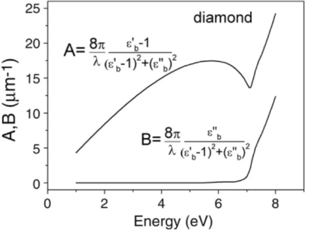
RβFig. 1. A and B coefficients for diamond bulk as a function of photon energy, computed from optical data in Ref. [26]. For definition of A and B see also Ref. [20].
where Rαand Rβare the intensities of reflected light for polarization along the
α
· and
β
orthogonaldirections. For the (1
×
1)-2×
1 reconstructions of C, Si and Ge,α
· and
β
mean the [0¯
11] and [211]
¯
directions, respectively parallel with and perpendicular to the chains of Pandey’s model [3].A model is necessary to relate a RAS spectrum to (the anisotropy of) the surface dielectric function
∆
ε
s=
∆ε
s0−
i∆ε
00
s: within the classical three-layer dielectric model [19], it is possible to demonstrate
that (being d the thickness of the surface layer)
∆R
/
R=
d[
A∆ε
00s−
B∆ε
0s]
(2)where A and B (for definition, see Ref. [20]) are coefficients depending only upon bulk dielectric properties, and are computed from data in literature. A and B for bulk diamond have been reported inFig. 1. B is nearly null up to 7 eV: consequently, the second term in RAS expression, proportional to the real part of the surface dielectric function anisotropy, vanishes in this range, and RAS yields just the anisotropy of the imaginary part of the surface dielectric function∆
ε
s00[20] even above the region of bulk transparency (the diamond gap is∼
5.
5 eV).We have used both the standard Aspnes’ version of the RAS spectrometer [17,21] — where light emerging from the sample is analyzed by a (second) polarizer — and the so-called ‘‘Russian’’ version of RAS (i.e. without analyzer) [16,17,22]. This latter option turned out to be particularly useful, especially on account of the strong birefringence of natural diamond [23]. Three different RAS apparatuses, almost completely homemade, were employed to cover the total energy range from 0.4 to 2.8 eV (for details see Ref. [7]).
3. Results and discussion
For the particular shape of our sample (the two faces are not perfectly parallel), in the bulk transparency region we had the possibility of measuring separately two beams: one (hereafter cited as B1) is reflected at the sample surface (separating vacuum and diamond bulk), the other (B2) is reflected at the rear surface (separating diamond bulk and vacuum) crossing twice the whole sample (see the inset inFig. 2). InFig. 2we present the RAS spectrum measured at the clean single-domain C(111)-2
×
1 surface, collecting the beam B1 in the range 0.3–2.8 eV. The corresponding LEED picture (not reported) clearly exhibited the 2×
1 reconstruction [7]. The RAS curve (already published in Ref. [7]) has been obtained after subtraction of a reference spectrum (in this case, measured at the oxidized surface) from the spectrum of the clean surface, in order to eliminate spurious signals due to residual anisotropy of the optical system.The spectrum inFig. 2shows a peak in∆R
/
R at 1.
47±
0.
02 eV, with an intensity slightly lower than 2×
10−2. At lower photon energies, in the region below the peak down to 0.4 eV∆R/
R is null, excludingFig. 2. (a) (left axis, full line) experimental∆R/R as a function of photon energy for a single-domain C(111)-2×1 surface, in the energy range from 0.4 to 2.8 eV, obtained measuring beam B1 (see text) and subtracting the curve of the oxidized surface from the curve of the clean surface. For the sign of∆R/R see Eq.(1)and related text. This spectrum has been taken from Ref. [7]; (b) (right axis, dotted line) imaginary part∆ε00
sof the dielectric function anisotropy for the clean C(111)2×1 surface, computed
from experimental∆R/R by Eq.(2)(see text) and multiplied by d, the ill-defined thickness of the surface layer. In the inset: sketch of the diamond sample to illustrate the beams B1 and B2 reflected at two different vacuum/diamond interfaces. The separation of two beams has been exaggerated for the reader.
the presence of detectable structures within the experimental sensitivity (which is about 1
×
10−4in this range, and becomes slightly worst, 3
×
10−4, above 1 eV). New, forthcoming experiments willbe dedicated to investigate the range above 2.8 eV. Preliminary results have shown that there the anisotropy is small, although not null, but no well-defined structures have been detected.
In the same figure, we have also drawn the imaginary part∆
ε
00sof the dielectric function anisotropy
for the clean C(111)2
×
1 surface, computed from experimental∆R/
R by Eq.(2). In the figure (where∆
ε
00s has been multiplied by the surface thickness d, an ill-defined parameter) the peak is slightly
red-shifted in energy with respect to∆R
/
R (here at 1.45 eV) due to the energy dependence of coefficient A.The surface origin of the∆R
/
R peak at 1.47 eV is substantiated by very strong arguments: (i) itappears just after the 2
×
1 phase has been prepared, as shown by LEED: before the final annealing, the spectrum is completely structureless in the same photon energy region; (ii) its energy position lies well inside the gap of the bulk diamond: in particular, the presence of structures below 7 eV should be attributed to optical transitions between surface bands, due to the role of A and B coefficients (seeFig. 1) in the formula for∆R
/
R (see Eq.(2)); (iii) it is sensitive to gas contamination, and disappears progressively during exposure of the sample to high purity molecular oxygen introduced in the chamber (the complete disappearance occurs at about 2×
104L, where 1 L=
1×
10−6Torr s);(iv) alternative explanations (as due, for example, to steps of the clean surface) can be ruled out [7]. The clear identification of the surface gap represents a fundamental goal: although the pioneering experiment of Pepper [8] is certainly valuable, the present result demonstrates above any doubt that
a gap between surface states exists, that is related to the 2
×
1 reconstruction, and measures its value with a precision never reached before.The resemblance with the dangling bonds peak of Si and Ge(111)2
×
1 [1,2] is impressive. In particular, from the comparison with the surface peak measured after cleavage by RAS in Si(111)2×
1 at 0.45 eV [18] — in its turn practically coincident with the celebrated peak measured by SDR on the same surface [2] –, it is very apparent that both curves exhibit a very similar slightly asymmetric lineshape. Also the character of the anisotropy is identical: higher reflectivity for electric field along the [011] direction, that is along the chains of the reconstruction single-domain. For symmetry¯
reasons [2], this means that the transitions giving rise to the peak at 1.47 eV occur along the JK line of the surface Brillouin zone. Both these facts (lineshape and polarization dependence) strongly push towards the conclusion that the diamond cleavage surface is also reconstructed according to the Pandeyπ
-bonded model [3], largely accepted nowadays for Si and Ge.At the same time, however, new important questions raise. At first, the experimental value of the gap is markedly higher than the theoretical one (1.5 eV against less than 1 eV) [12,13]. Additionally, the experimental value could contain an excitonic term, pushing the true value of the gap towards higher values (as it happens for Si(111)2
×
1). In C(001)2×
1, an exciton having a very large binding energy value (about 1 eV) has been proposed [24].The gap value is not the only problem, as it is not clear which is the mechanism opening the gap: both buckling and dimerization of the chain seem to fail, a fact that sounds surprising when the comparison with Si and Ge is considered. However, this disagreement should not reduce the significant result obtained in Ref. [12]: the successful opening of a gap between surface states. The unquestionable difference between experiment and theory could suggest that some significant inadequacy exists in our understanding of the clean C(111)2
×
1. An important test will be represented by the measurement of the total anisotropy of the surface reflectivity signal: this cannot be obtained from RAS, but – as for Si and Ge(111)2×
1 – from a different optical technique, Surface Differential Reflectivity (SDR) with polarized light [1,2]. For comparison, in Si and Ge the experimental value of anisotropy coming from SDR is 100% and 88%, respectively (due to the different one-dimensional character of electronic states along the chains) [2]: for C(111)2×
1 we suppose an anisotropy value in the same range. SDR experiments are in progress, by using either polarized or unpolarized light (the latter condition will not limit the investigation to single domain surfaces). Results are still preliminary, nevertheless we suggest a possible speculation: it is plain that a close coincidence between RAS and SDR spectra – as for Si and Ge(111)2×
1 – would push a new, stringent argument to strengthen the Pandey model for the surface reconstruction. In this case, the theoretical problem could be labeled as a technical question, related to computational procedures and approximations [13]. But if SDR results should show an evident difference with respect to RAS, for example if the surface peak is not completely polarized because of the presence of a large isotropic contribution, the problem will appear connected to more deep motivations, as the validity of the reconstruction model assumed for the 2×
1 diamond surface.Before concluding, we dwell on an apparently minor experimental detail. We have already mentioned the opportunity we had to use the only known single-domain C(111) sample: now we repeat that also the particular shape of the sample has been important (see beginning of Section3). InFig. 3, we report – from a different RAS experiment and in a reduced photon energy range with respect toFig. 2– both spectra measured collecting, separately, the beam B1 and the beam B2. Also in this case we have subtracted from each curve the spectrum of the fully oxidized surface. It is evident that the positive curve [beam B1, meaning
(
∆R/
R)
B1], peaked at about 1.48 eV (in agreementwithFig. 2, within experimental accuracy), presents a lower anisotropy value thanFig. 2: this is the consequence of a deteriorated quality of the sample, due to the repeated annealing treatments and oxidation procedures [25], also demonstrated by the worse related LEED patterns. To recover a higher anisotropy signal, a new, extensive manual polishing has been necessary. The negative curve [beam B2,
(
∆R/
R)
B2] has a minimum at the same energy of the B1 maximum (1.48 eV). Two distinctivedifferences clearly emerge from the comparison with the B1 curve: (i) the spectrum is now all negative, (ii) the amplitude absolute value (that is the anisotropy) is larger.
When the classical Aspnes–McIntyre three-layer model [19] is applied to both configurations – yielding
(
∆R/
R)
B1or(
∆R/
R)
B2, respectively – it is straightforward to obtain thatFig. 3. ∆R/R as a function of photon energy for a single-domain C(111)-2×1 surface (of lower quality, with respect toFig. 2), in the energy range 1.2 to 1.7 eV. The positive curve refers to beam B1, the negative curve to beam B2 (for details, see text). In all cases, each curve has been obtained subtracting the spectrum measured after the complete oxidation (about 2×10⁴L of molecular oxygen) from the spectrum measured at the clean surface.
(
∆R/
R)
B2= −
n(
∆R/
R)
B1 (3)where n is the refractive index of diamond bulk in the transparency region. FromFig. 3, one obtains that, at 1.48 eV,
(
∆R/
R)
B2/(
∆R/
R)
B1= −
2.
8. This result should be compared with the value n∼
2.
4 for the diamond refractive index [26]. The qualitative agreement (B1 positive, B2 negative) is evident; the quantitative agreement (within 15%) is satisfactory, considering the uncertainties affecting the B2 experimental data (mostly the bulk birefringence [23]). We stress a noteworthy corollary of this result: if both beams are merged on the detector (it happens if the sample is not accurately shaped to separate them) the total anisotropy effect would present an opposite sign with respect to the correct one, for the partial compensation of two curves. If the sign of the optical anisotropy were related to the directions of the carbon atoms chains (known by LEED), in this case the anisotropy would be interpreted as not consistent with the Pandey model, causing a trivial but noteworthy mistake.In conclusion, RAS experiments on a single-domain diamond C(111)-2
×
1 surface have allowed for the first time to measure accurately the optical gap between dangling-bond states. Differently from other group IV surfaces, the experimental result for the optical gap is in plain disagreement with the most recent band calculations results, at the moment unable to account for such a large energy gap value (even higher for possible excitonic effects). Moreover, the physical origin of that gap is not explained yet, for a second time in variance with the Si and Ge cleavage surfaces. Although the reason for this is still under debate, a possible modification of the reconstruction model assumed for the 2×
1 surface should be also evaluated. Further experimental investigations could offer significant information to solve the last fascinating puzzle of this surface: in particular, SDR experiments, to evaluate the total optical anisotropy of the surface, and atom-resolved imaging of the reconstructed surface. To that end, we have also discussed in detail minor experimental results, as the∆R/
R(presenting opposite polarizations and different amplitudes) shows that a wrong interpretation of data would be otherwise possible.
Acknowledgements
The whole list of colleagues acknowledged for this work is reported elsewhere [7]. Here we recall that F. van der Veen has given the sample, and that M. Rebak of iThemba LABS (Gauteng, South Africa) did the ‘‘hard’’ mechanical polishing of the sample.
References
[1] G. Chiarotti, Surf. Sci. 299–300 (1994) 541, and references therein; P. Chiaradia, R. Del Sole, Surf. Rev. Lett. 6 (1999) 517, and references therein. [2] P. Chiaradia, et al., Phys. Rev. Lett. 52 (1984) 1145;
G. Chiarotti, et al., Surf. Sci. 453 (2000) 112. [3] K.C. Pandey, Phys. Rev. Lett. 47 (1981) 1913;
K.C. Pandey, Phys. Rev. B 25 (1982) 4338.
[4] P.G. Lurie, J.M. Wilson, Surf. Sci. 65 (1977) 453, and references therein. [5] T.E. Derry, L. Smit, J.F. Van der veen, Surf. Sci. 167 (1986) 502. [6] R. Graupner, et al., Phys. Rev. B 55 (1997) 10841.
[7] G. Bussetti, et al., Europhys. Lett. 79 (2007) 57002. [8] S.V. Pepper, Surf. Sci. 123 (1982) 47.
[9] D. Vanderbilt, S.G. Louie, Phys. Rev. B 30 (1984) 6118. [10] W.G. Schmidt, A. Scholze, F. Bechstedt, Surf. Sci. 351 (1996) 183. [11] C. Kress, M. Fiedler, F. Bechstedt, Europhys. Lett. 28 (1994) 433. [12] M. Marsili, et al., Phys. Rev. B 72 (2005) 115415.
[13] M. Marsili, et al., Phys. Rev. B 78 (2008) 205414. [14] W.J. Huisman, et al., Surf. Sci. 396 (1998) 241;
W.J. Huisman, J.F. Peters, J.F. Van der veen, Surf. Sci. 396 (1998) 253. [15] D.E. Aspnes, Thin Solid Films 233 (1993) 1, and references therein. [16] V.L. Berkovits, et al., Solid State Commun. 56 (1985) 449. [17] P. Weightman, et al., Rep. Prog. Phys. 68 (2005) 1251. [18] C. Goletti, et al., Phys. Rev. B 66 (2002) 153307. [19] J.D.E. Mcintyre, D.E. Aspnes, Surf. Sci. 24 (1971) 417. [20] C. Goletti, et al., J. Phys.: Condens. Matter. 16 (2004) S4289. [21] D.E. Aspnes, et al., J. Vac. Sci. Technol. A 6 (1988) 1327. [22] A. Salvati, P. Chiaradia, Appl. Opt. 39 (2000) 5820.
[23] J.E Field (Ed.), Properties of Diamond, Academic Press, London, 1979; G. Davies, Diamond, Adam Hilger Ltd, Bristol, 1984.
[24] M. Palummo, et al., Phys. Rev. Lett. 94 (2005) 87404. [25] K. Bobrov, et al., Appl. Surf. Sci. 196 (2002) 173.