UNIVERSITY
OF TRENTO
DIPARTIMENTO DI INGEGNERIA E SCIENZA DELL’INFORMAZIONE
38050 Povo – Trento (Italy), Via Sommarive 14 http://www.disi.unitn.it
SUPERFICIAL BREAKDOWN ANALYSIS IN 3D DETECTORS AND
IN ACTIVE-EDGE PLANAR DETECTORS THROUGH TCAD
SIMULATIONS
Marco Povoli
June 2009
Contents
Introduction 1
1 3D Technology 3
1.1 3D Detectors made in Trento . . . 3
1.1.1 3D-STC - Single Type Column . . . 3
1.1.2 3D-DDTC - Double Sided Double Type Column . . . 4
1.2 Active edge detectors . . . 5
1.3 Fabrication process . . . 6
1.3.1 3D-DDTC - Fabrication process . . . 6
1.4 Possible applications . . . 7
2 C.A.D Instruments 9 2.1 Synopsys - Advanced TCAD Tools . . . 9
2.2 MDRAW . . . 9
2.3 Sentaurus Device . . . 10
2.3.1 Simulations . . . 11
2.4 Tecplot SV . . . 11
2.5 Inspect . . . 11
3 Simulations and final results 13 3.1 3D-DDTC Detector . . . 13
3.1.1 Simulated structures . . . 14
3.1.2 Type of simulations . . . 14
3.2 Active-edge planar detector . . . 16
3.2.1 Simulated structures . . . 16
3.2.2 Type of simulations . . . 16
3.3 Results - 3D-DDTC Detector . . . 18
3.3.1 Gradual addition of all the elements of the structure . . . 18
3.3.2 Inter-electrode distance variation . . . 20
3.4 Results - Planar active-edge detector . . . 22
3.4.1 Variation of the distance between the active-edge and the pla-nar electrode . . . 23
3.4.2 Field plate . . . 24
3.4.3 Oxide thickness modification . . . 27
3.4.4 Reversed structure . . . 29
3.4.5 Floating region . . . 29
3.4.6 Charge collection analysis . . . 31
Conclusions 37
List of Figures
1.1 3D-STC . . . 4
1.2 3D-DDTC . . . 5
1.3 Electric field distribution at 5V e 30V of bias . . . 5
1.4 Main steps of the 3D-DDTC fabrication processs on n-type substrate. 7 1.5 Utilizzo del wafer di supporto . . . 7
2.1 MDRAW’s main window . . . 10
3.1 3D-DDTC - Simulated structure . . . 15
3.2 Planar active-edge detector . . . 17
3.3 3D-DDTC - N type lateral diffusion - Superficial charge concentration 5 × 1011cm−2 - Results . . . 19
3.4 3D-DDTC - P type lateral diffusion - Superficial charge concentration 5 × 1011cm−2 - Results . . . 20
3.5 Corner region . . . 23
3.6 Field-plate . . . 25
3.7 Breakdown voltages vs. Oxide thickness . . . 28
3.8 Floating region . . . 30
3.9 Behavior of the floating region . . . 31
3.10 X-photon in the top left region . . . 33
3.11 X-photon in the bottom left region . . . 34
3.12 MIP particle in the left region . . . 35
List of Tables
3.1 3D-DDTC - Structures characteristics . . . 14
3.2 Dimension and characteristic of the simulated structure for the planar active-edge case . . . 16
3.3 Summary of the breakdown voltages obtained after the simulations . 21 3.4 Breakdown voltages for the constant P-type lateral diffusion case . . 22
3.5 Breakdown voltages for the constant N-type lateral diffusion case . . 22
3.6 Simple configuration - Results. . . 24
3.7 Breakdown voltages d=10 µm - field-plate . . . 26
3.8 Breakdown voltages d=20 µm - field-plate . . . 26
3.9 Breakdown voltages d=30 µm - field-plate . . . 27
3.10 Oxide thickness modification - Results . . . 28
3.11 Reversed structure - Results . . . 29
3.12 Floating region - Results . . . 30
Introduction
This report describes the main results obtained from numerical simulations of silicon detectors with tridimensional electrodes and with active-edge and planar electrodes. The first type of detector, only recently proposed thanks to the great improvement of the micromachining processes, has electrodes penetrating vertically in the substrate. Differently from the conventional planar detectors in which the charge collection occurs on the surface of the device, the 3D architecture allows to decouple the active volume of the detector, determined by the thickness of the silicon wafer, from the distance that the carriers need to travel to be collected from the electrodes. This distance is equal to the one between the electrodes and can be reduced in the order of some ten of micrometers. This property allows to obtain very fast detectors that are, at the same time, very resistant to radiation damage, to be used in the particle tracking systems of the next generation’s accelerators.
The second type of detectors combines planar structures with the 3D technology. They essentially are planar photodiodes but an active-edge is added using the 3D technology. Whit this trick it is possible to reduce the dead area around the device, ensuring less area waste and better distribution of the detectors on wide surfaces.
The activity was focused on numerical simulations with particular attention to the breakdown dynamics, in order to understand how the phenomena occurs and to gain better knowledge of the critical areas of the devices before their realization in the FBK laboratories. The simulations were carried out applying an increasing reverse voltage to the devices and looking at the regions where the electric field is maximum. In the active-edge case, different configurations were tested in order to understand which one allowed to apply the higher voltage. At the end some transient simulations were made to assure that the introduction of the active-edge didn’t compromise the charge collection in the detectors.
Chapter 1
3D Technology
The first planar silicon detectors were developed in the ’60s while in the ’80s the first devices with planar electrodes made by ionic implantation were presented. In both cases the electrodes were planar and the full depletion voltages were in the order of many tens of volts. Planar detectors are still employed in many fields but, for some critical applications like high energy physics, they are less performant than the more recent proposed detectors.
The technology that seems to be nowadays more interesting, is the so called ”3D Technology”, which is the one that allows to build electrodes penetrating vertically in the substrate of the detector passing completely through it, drastically reducing the distance free carriers need to travel to be collected. Another advantage of the 3D technology lies in the possibility to realize ”active-edge silicon detectors” with minimum dead area.
The first proposal of a 3D silicon detector was made by Sherwood Parker in 1997 [1].
1.1
3D Detectors made in Trento
In Trento there is a research project in the ambit of the 3D silicon detectors. This project is a collaboration between FBK and INFN. The first part of the project was focused on the production of some less complicated 3D detectors and then on gradually increasing the complexity, in order to reach a ”full-3D” device. Some of the architectural solution adopted in Trento are here reported.
1.1.1
3D-STC - Single Type Column
The denomination of these detectors comes from the fact that the columns are of one doping type only (STC - Single Type Column). The idea and the first results are presented in [2, 3, 4]. The single column configuration allows to simplify the production process because the holes are etched and doped in only one step and, because they are not completely passing through the substrate, there’s no need to
Figure 1.1: 3D-STC
use a support wafer. The choice was to not entirely fill the holes with the dopant, in order to further simplify the process. An example is shown in figure 1.1: the substrate is P-type and the electrodes are N+-type, the ohmic contact is made with
a constant P+ diffusion on the back side.
The main disadvantage of this configuration lies in the fact that it doesn’t allows to control the electric field intensity with the applied voltage once full depletion is reached. The only choice is to use the bulk dopant concentration that will lead to the desired electric filed intensity, but this is only possible during the design phase. This problem leads to low field region that are large, causing a degradation in the device’s performances.
1.1.2
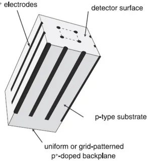
3D-DDTC - Double Sided Double Type Column
In order to assure better performances and at the same time maintain the process complexity low, in [5] a new type of detector is presented. The denomination 3D-DDTC comes from the fact that the electrodes are of two different doping type and are etched from both sides of the wafer. An example is reported in figure 1.2. These detectors have holes diameter equal to 10 µm and the distance between them is variable during the design phase. The substrate is P-type, the junction columns are etched from the top surface while the ohmic ones are etched from the bottom surface. The output signal is read from the N+ electrodes while the P+ electrodes are all connected together by a P diffusion and metallization on the back surface.
The main disadvantages of this configuration reside in the lack of an active-edge and in the fact that the electrodes are empty and therefore dead regions. This second problem can be partially solved tilting the detector by some degrees with respect to the incident radiation. In terms of signal efficiency and radiation hardness a result
1.2. ACTIVE EDGE DETECTORS 5
Figure 1.2: 3D-DDTC
Figure 1.3: Electric field distribution at 5V e 30V of bias
comparable with the one of full 3D detectors is expected. A critical regions is located under the tip of the electrode, where the electric field’s intensity is lower.
1.2
Active edge detectors
The use of 3D technology allows to build silicon detectors with minimum dead area along the edges both with planar and 3D electrodes. This is done by etching trenches around the detectors (instead of saw-cutting it) using the DRIE etching procedure. This procedure allows to reduce the dead area around the devices in the order of few micrometers but can cause some problems from the break-down point of view because the polarized structures are now closer to each other. The fabrication process is more difficult and a support wafer is required to assure the integrity of the devices along the entire procedure. The main advantage resides in the possibility of less area waste when many detectors are placed on wide surfaces.
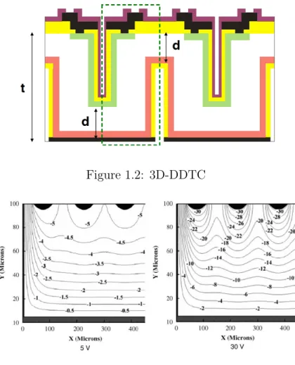
The active-edge can be built both with 3D and planar detectors. Some results are reported in [6] for planar active-edge devices. The electric field distribution is shown in figure 1.3. The full depletion is reached for 5V.
In a structure like the one shown in 1.3, with N+ edge and N substrate, some problems in reaching full depletion are found. The corner regions cannot be
com-pletely depleted. To change this situation it is better to realize the P-N junction along the active-edge and the ohmic contact with the planar structures. This also leads to lower electric field intensity in the structure.
1.3
Fabrication process
The fabrication process for a 3D detector is long and complicated and it involves some non conventional steps. Later the full process is described from an high level point of view.
1.3.1
3D-DDTC - Fabrication process
The following fabrication process is the one used in the FBK laboratories. The reference for this process are [5] in relation to the fabrication of the 3D-DTC-1 batch. The substrate is N-type with a wafer thickness equal to 300µm, the column depth is 180µm and the inter-strip distance is 80/100µm. The most important steps of the process are the following and are shown in figure 1.4:
1. A thick oxide is grown, to be used as a masking layer for the DRIE step on the back side. The oxide is patterned on the back side and first DRIE step is performed.
2. The thick oxide layer is removed from the back side and Phosphorus is diffused from a solid source into columns and at the back surface to obtain a good ohmic contact. A thin oxide layer is later grown to avoid out-diffusion of the dopant.
3. The oxide layer on the front side is patterned and the second DRIE step is performed for the column etching.
4. The thick oxide layer on the front side is removed from a ring shaped region surrounding holes; Boron is diffused from a solid source into the columns and at the open surface region to ease contact formation.
5. An oxide layer is grown at the surface and in the columns to prevent the dopant out-diffusion; an additional oxide layer (TEOS) is deposited; then, contact holes are defined and etched through the oxide at the surface; aluminum is sputtered and patterned.
6. The final passivation layer is deposited on the front side, whereas on the back side, after removal of the oxide layer, aluminum sputtering provides a uniform metal electrode. Finally, the passivation layer on the front side is patterned to define the access regions to the metal layer.
1.4. POSSIBLE APPLICATIONS 7
Figure 1.4: Main steps of the 3D-DDTC fabrication processs on n-type substrate.
Figure 1.5: Utilizzo del wafer di supporto
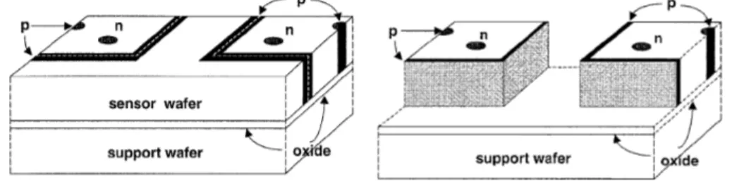
In order to fabricate full-3D detectors with active-edge, a sacrificial wafer is needed to prevent from cracks during the process and to keep any fully diced parts in place during the final fabrication steps. An example of the use of the support wafer is visible in figure 1.5.
1.4
Possible applications
The field of application of the 3D detectors is mainly in high energy physics exper-iments; thanks to their innate radiation hardness, they are a suitable solution for the Inner Tracking Systems in the next generation’s particle accelerators (sLHC).
They are also suitable for all those applications that require high efficiency in X-Rays detection and fast readings, in particular digital radiography application in medical or industrial ambit.
The possibility to work at ambient temperature, allows the fabrication of cheap portable devices to monitor radiation in the environmental control field.
Other possible applications are related to synchrotron light experiments in DNA sequencing. It is also possible to use the 3D detectors to study molecular structures. As last note it is possible to say that these detectors, thanks to their fast signal reading, could be suitable in short range optical communications and in advanced imaging systems.
Using the active-edge structure it is possible to obtain a better redistribution of the detectors on wide surfaces in medical imaging applications.
Chapter 2
C.A.D Instruments
A brief description of the utilized CAD instruments will be here briefly reported. In this activity the Synopsys TCAD suite has been used [7].
2.1
Synopsys - Advanced TCAD Tools
The Synopsys TCAD suite includes fabrication and functional simulation instru-ments for silicon devices. Some data analyzing tools are also included. They support an high quantity of different devices like CMOS, power devices, memories, sensors, solar cells, RF analog devices. In order to simulate some kind of device the following steps must be performed:
1. Structure definition using ”MDRAW”
2. Device simulation using ”Sentaurus Device”
3. Results analysis with Tecplot and Inspect.
In the following the basic features of these tools are reported.
2.2
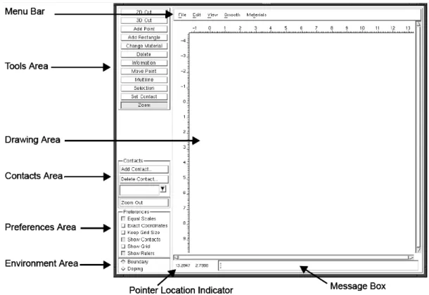
MDRAW
Mdraw is very flexible 2D structure creation software. It includes 2D engines for mesh creation. This program offers the possibility to work with the ”Tool command language (tcl)” from command line.
Mdraw includes: • Boundaries editor
• Doping and grid editor
• Tcl interpreter
• 2D meshing engine.
Figure 2.1: MDRAW’s main window
In order to launch the program the user must enter the command ”mdraw” from the command line.
The program is divided essentially in two environments: in the first one the user can create and modify the structure’s boundaries while, in the other one, the user can add doping profiles, the grid and its eventual refinement. The main MDRAW window is shown in figure 2.1.
2.3
Sentaurus Device
Sentaurus Device numerically simulates the electrical behavior of a single semicon-ductor device or multiple devices combined in a circuit. Currents, voltages and charge concentrations are evaluated on the base of a series of physical equations describing carriers distribution and conduction mechanisms. A real semiconduc-tor device is represented as a virtual device whose properties are discretized on a numerical grid. Each structure is here described with two files:
• the grid file (*.grd) containing node positions, boundaries, materials and con-tacts of the device;
• the data file (*.dat) containing device’s properties like doping profiles.
Sentaurus Device has many characteristics:
2.4. TECPLOT SV 11 • Support for different geometries (1D, 2D, 3D and 2D in cylindrical
coordi-nates).
• Wide set of non linear solvers.
• Mixed simulation mode between mesh based detectors and Spice models.
2.3.1
Simulations
Two different modalities for the launch of simulations exits:
• from command line.
• from Sentaurus Workbench.
In this report all the simulations are started from the command line:
s d e v i c e <command_file_name>
d e s s i s <command_file_name>
2.4
Tecplot SV
Tecplot is a visualization tools for 2D and 3D data with extended capabilities. Syn-opsys provides a personal Tecplot distribution which includes all Tecplot’s previous distributions and a special add on. Teclopt includes many improvements with re-spect to the previous versions of Tecplot-ISE and is now part of the ”Sentaurus Workbench Visualization”. In order to visualize simulation results the structure’s *.dat and *.grd files are requested.
2.5
Inspect
Inspect is a powerful instrument, capable of data analysis with scripting support and graphical interface. A curve in Inspect is defined by a sequence of data points organized in arrays (different arrays for x e y coordinates). Those arrays can be assigned to the graph’s axis to plot the saved curve. Inspect support many input formats. To visualize simulation’s results it necessary to load the *.plt files saved from Sentaurus Device.
Chapter 3
Simulations and final results
The first part of the activity was focused on 3D detectors with the columns com-pletely etched through the substrate in order to find the most critical region from the breakdown point of view.
The second type of simulations had as subject planar photodiodes with active-edge. The element under investigation was the optimal distance needed between the planar electrode and the active-edge, in order to have an high breakdown voltage. Many different configurations were tested with the intent to reduce the electric field’s intensity inside the structure.
Finally some transient simulation were performed, in order to understand if the introduction of the active-edge caused any problems from the charge collection point of view.
The final results are here reported.
3.1
3D-DDTC Detector
The particular layout solution implemented at FBK laboratories suggests that more attention should be paid to some aspects. As previously highligthed in chapter 1 in subsection 1.1.2, in this structure the columns are not completely filled with dopant so it is impossible to realize the metal contact on top of them. For this reason, in the superficial region, some lateral dopant diffusion are needed in order to connect the electrodes with the metal layer. These regions are part of the electrode and so they are polarized at high voltages. The presence of the lateral diffusions causes a decrease in the inter-electrode distance near the surface, facilitating the occurring of the breakdown. In this first run of simulations the focus is on two aspects:
1. Finding the most critical area in the structure (where the breakdown occurs earlier)
2. Finding an optimal electrode/lateral diffusion distance.
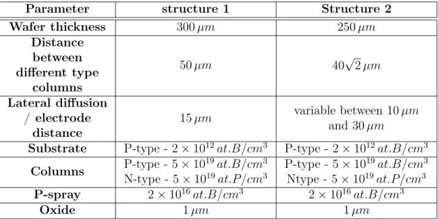
Parameter structure 1 Structure 2 Wafer thickness 300 µm 250 µm Distance between different type columns 50 µm 40√2 µm Lateral diffusion / electrode distance 15 µm variable between 10 µm and 30 µm
Substrate P-type - 2 × 10¹²at.B/cm3 P-type - 2 × 10¹²at.B/cm3 Columns P-type - 5 × 10
19at.B/cm3
N-type - 5 × 10¹⁹at.P/cm3
P-type - 5 × 10¹⁹at.B/cm3
Ntype - 5 × 10¹⁹at.P/cm3 P-spray 2 × 10¹⁶at.B/cm3 2 × 10¹⁶at.B/cm3
Oxide 1 µm 1 µm
Table 3.1: 3D-DDTC - Structures characteristics
The simulated structures are bi-dimensional and represents a cut along the diagonal of an elementary cell of a 3D detector.
3.1.1
Simulated structures
All the dimensions and relevant quantities are report in tab.3.1.
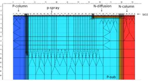
In figure 3.1 images from the top and bottom part of the structure are shown together with the grid refinement. Both structures have a superficial grid refinement to better evaluate the effects of the trapped charge inside the oxide layer, near the surface a slightly higher P doping is present in order to partially compensate the interface charge.
3.1.2
Type of simulations
The two structures are simulated with different modalities but the are both reverse biased applying a negative voltage ramp to the P column:
1. In the first case all the single elements composing the structures are separately added, in order to understand which one causes the most critical reduction in the breakdown voltage. The superficial inter-electrode distance is in this case constant.
2. In this case the complete structure is simulated, but the superficial inter-electrode distance is modified in order to identify an optimal value for this parameter and to understand if the breakdown occurs much easily in the top part or in the bottom part.
3.1. 3D-DDTC DETECTOR 15
(a) Parte superiore della struttura
(b) Parte inferiore della struttura
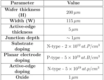
Parameter Value Wafer thickness (H) 200 µm Width (W) 115 µm Active-edge thickness 5 µm Junction depth ∼ 1µm Substrate doping N-type - 2 × 10 12at.P/cm3 Planar electrode doping P-type - 5 × 10 19at.B/cm3 Active-edge doping N-type - 5 × 10 19at.p/cm3 Oxide 1 µm
Table 3.2: Dimension and characteristic of the simulated structure for the planar active-edge case
3.2
Active-edge planar detector
In this case the focus is on the consequences that the insertion of the active-edge may imply. The simulated structure has a planar detector and an active-edge that completely surround the bulk. The biasing of the structure is performed using the ohmic contact along the active-edge. The manifestation of the breakdown is attended where the distance between the electrode and the edge is minimum. The target of this run of simulations is to identify an optimal value for this distance, allowing to apply high voltages to the device in order to completely deplete the substrate. The structure is bi-dimensional but different configurations are tested.
3.2.1
Simulated structures
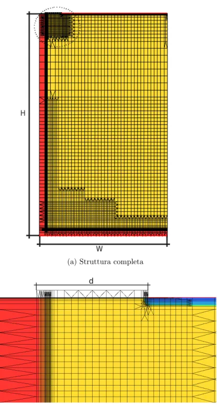
As already explained earlier the basic structure remains essentially constant in all the simulations, only some little change in the configuration will be made in order to obtain better results. In figure 3.2 two images are shown, one is the complete structure (figure 3.2a) and the other is an enlargement of the top left region which is the most interesting one (figure 3.2b). Dimensions and characteristics of the structure are reported in tab.3.2.
Only one half of the real structure is simulated to limit the number of nodes in the grid. The results are not affected by this fact. The ohmic contact is realized along the active-edge and the junction is realized with the planar electrode.
3.2.2
Type of simulations
3.2. ACTIVE-EDGE PLANAR DETECTOR 17
(a) Struttura completa
(b) Ingrandimento dell’angolo superiore sinistro
1. In the first case the distance between the planar electrode and the active-edge is modified. This is done for different superficial charge concentrations and for different structure configurations.
2. In the second case transient simulations are performed to understand how the active-edge affects the charge collection mechanisms. Two different types of radiations are simulated, X-photon and a MIP particle.
3.3
Results - 3D-DDTC Detector
The results for the 3D-DDTC are here reported with reference to the structure described in section 3.1. The reported results are only the most important ones and are taken from the most important regions of the structures (top and bottom).
3.3.1
Gradual addition of all the elements of the structure
To comprehend better the effects that each element has on the structure the better way is to add them one after the other. The distance between the electrode and the lateral diffusions (when present) is fixed to 15 µm. The results here reported are only the final ones in order to maintain the complexity of this report low, a table at the end of this section (tab.3.3) will show all the results, but for more comprehensive description refer to [8].
Complete structure with the only N lateral diffusion
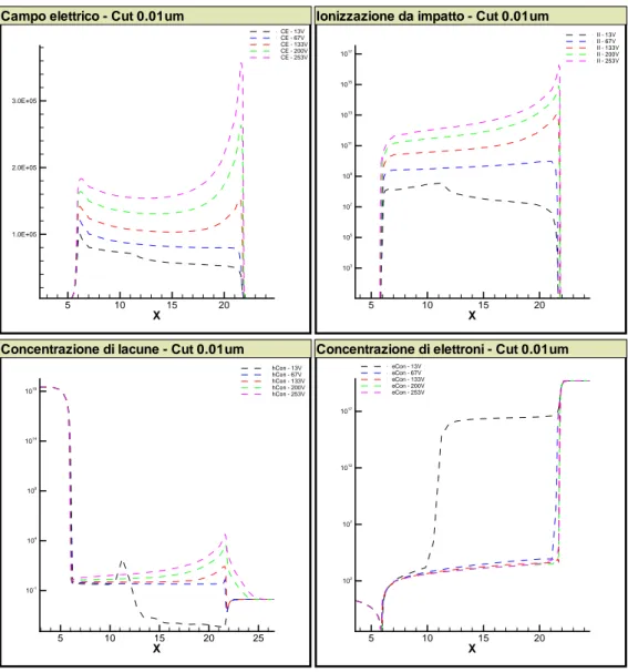
The following results are obtained for a superficial charge concentration of 5 × 1011cm−2. All the curves are obtained from sectioning the structure 0.01µm from
the top surface. The breakdown voltage is around 260V. The reported curves in figure 3.3 are related to bias voltages equal to: 13 V, 67 V, 133 V, 200 V and 253 V. As expected the maximum of the electric field is located on the tip of the N lateral diffusion but it is possible to notice a slight maximum on the right for lower bias voltages. This is due to the presence of an high charge concentration near the surface that is most likely completely compensating the p-spray layer. The maximum of the impact ionization is also on the tip of N lateral diffusion and this confirms that the breakdown occurred in this region. The effect is magnified from the fact that the lateral diffusion has a strong curvature that facilitates the manifestation of the phenomena.
Complete structure with the only P lateral diffusion
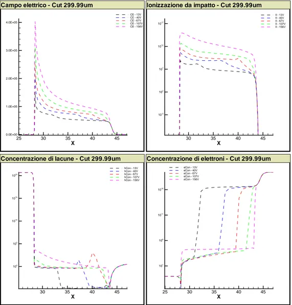
The following results are obtained for a superficial charge concentration of 5 × 1011cm−2. All the curves are obtained from sectioning the structure 0.01µm from
3.3. RESULTS - 3D-DDTC DETECTOR 19 X 5 10 15 20 1.0E+05 2.0E+05 3.0E+05 CE - 13V CE - 67V CE - 133V CE - 200V CE - 253V Campo elettrico - Cut 0.01um
X 5 10 15 20 103 105 107 109 1011 1013 1015 1017 II - 13V II - 67V II - 133V II - 200V II - 253V Ionizzazione da impatto - Cut 0.01um
X 5 10 15 20 25 10-1 104 109 1014 1019 hCon - 13V hCon - 67V hCon - 133V hCon - 200V hCon - 253V Concentrazione di lacune - Cut 0.01um
X 5 10 15 20 102 107 1012 1017 eCon - 13V eCon - 67V eCon - 133V eCon - 200V eCon - 253V
Concentrazione di elettroni - Cut 0.01um
Figure 3.3: 3D-DDTC - N type lateral diffusion - Superficial charge concentration 5 × 1011cm−2 - Results
X 25 30 35 40 45 0.0E+00 1.0E+05 2.0E+05 3.0E+05 4.0E+05 CE - 13V CE - 40V CE - 67V CE - 107V CE - 156V Campo elettrico - Cut 299.99um
X 30 35 40 45 10-3 102 107 1012 1017 II - 13V II - 40V II - 67V II - 107V II - 156V Ionizzazione da impatto - Cut 299.99um
X 30 35 40 45 100 105 1010 1015 1020 hCon - 13V hCon - 40V hCon - 67V hCon - 107V hCon - 156V Concentrazione di lacune - Cut 299.99um
X 25 30 35 40 45 101 106 1011 1016 eCon - 13V eCon - 40V eCon - 67V eCon - 107V eCon - 156V
Concentrazione di elettroni - Cut 299.99um
Figure 3.4: 3D-DDTC - P type lateral diffusion - Superficial charge concentration 5 × 1011cm−2 - Results
the top surface. The breakdown voltage is around 164V. The reported curves in figure 3.4 refers to bias voltages equals to: 13 V, 40 V, 67 V, 107 V and 160 V.
The peak of the electric field is located in the left part of the structure at the tip of the P-type lateral diffusion. The superficial electrons concentration near the lateral diffusion is in fact higher than the one at the junction between the substrate and the N-type column. The really low breakdown voltage could be the result of a combination of the curvature effect of the lateral diffusion and the increase of the carriers in the critical region.
3.3.2
Inter-electrode distance variation
This type of simulations is executed maintaining one of the two lateral diffusions at a constant length while moving the other in order to understand which one, between the top and the bottom region of the structure, is more critical from the breakdown point of view. The charge concentration at the silicon/oxide interface
3.3. RESULTS - 3D-DDTC DETECTOR 21
Structure configuration Oxide charge [cm−2]
Voltage [V]
Only columns n.p. -700
Columns and p-spray n.p. -630 1 × 10¹¹ -676 Complete structure without
lateral diffusions 3 × 10
11 -710
5 × 10¹¹ -610 Columns and N-type diffusion n.p. -230 Columns and P-type diffusion n.p. -206 Columns, p-spray and N-type
diffusion n.p. -158
Columns, p-spray and P-type
diffusion n.p. -258
1 × 10¹¹ -186
Complete structure with N
diffusion 3 × 10
11 -230
5 × 10¹¹ -260
1 × 10¹¹ -245
Complete structure with P
diffusion 3 × 10
11 -208
5 × 10¹¹ -164
structure d[µm] Breakdown Voltage[V] Constant P-diff 10 149 Constant P-diff 15 189 Constant P-diff 20 212 Constant P-diff 25 244 Constant P-diff 30 278
Table 3.4: Breakdown voltages for the constant P-type lateral diffusion case
Structure d[µm] BreakdownVoltage[V] Constant N-diff 10 180 Constant N-diff 15 242 Constant N-diff 20 278 Constant N-diff 25 278 Constant N-diff 30 278
Table 3.5: Breakdown voltages for the constant N-type lateral diffusion case
will be constant and equal to 1 × 1011cm−2. The data are extracted 0.01µm from
the surfaces. The variation of the lateral diffusion/electrode distance will be made with 5µm steps in the 10 − 30µm range.
Only the final results are reported because the behavior of the structure is the same seen in the previous section. For more details refer to [8].
It seems that the most critical region of the structure is the upper one where the N-type lateral diffusion is present because the breakdown seems to be occurring earlier in this region. It is possible to say that a good value for ”d” is around 20µm.
3.4
Results - Planar active-edge detector
This run of simulation will be focused on a different type of detector and will have the target of finding the better architectural configuration for it, in order to have higher breakdown voltage as possible. In this case the full depletion voltage will be larger because the depletion region extends vertically and the region to deplete will be 200µm thick.
The basic structure is described in section 3.2 (figure 3.2 and tab.3.2). The ohmic contact is located along the active edge and the junction is formed with the planar electrode. Different superficial charge concentrations will be tested.
The investigation is focused on finding the optimal value for ”d”, in order to delay the inverse discharge. Starting from the simple configuration some different tricks will be tested to reduce the electric field peak in the structure. The attended behavior is similar to the one of semiconductor diode. The most critical region is located in the top left part of the structure.
3.4. RESULTS - PLANAR ACTIVE-EDGE DETECTOR 23 X Y 0 10 20 30 40 50 160 180 200 220 ElectrostaticPotential 3.4E+02 3.3E+02 3.0E+02 2.6E+02 2.3E+02 1.9E+02 1.5E+02 Linee di potenziale nella regione d’angolo
X Y 0 10 20 30 40 50 160 180 200 220 eDensity 1.0E+15 7.3E+11 5.4E+08 3.9E+05 2.9E+02 2.1E-01 Concentrazione di elettroni nella regione d’angolo
Figure 3.5: Corner region
3.4.1
Variation of the distance between the active-edge and
the planar electrode
The inverse voltage is applied to the active edge and the depletion of the bulk occurs in vertical direction. The full depletion is not possible in the corners of the active edge; in figure 3.5 it is possible to see this phenomena: on the left the potential lines in the structure are shown and on the right the concentration of the electrons is visible.
After this observation it is possible to look at the behavior in the top part of the structure. The ”d” parameter will be modified in order to find the better solution.
Simple configuration - Results
Only the values of the breakdown voltage are reported. The electric field peak in the structure is on the curvature of the P-N junction and is much higher if ”d” is small. The results are reported in tab.3.6. All the values seem to converge to a common low value for all the cases while the superficial charge concentration increases. This aspect could be very critical in post irradiation case, where the full depletion voltage will be higher; the risk is to not be able to fully deplete the detector before reaching the breakdown.
Active-edge / electrode distance Superficial Charge [cm−2] Breakdown voltage [V] 1 × 10¹¹ 127 10µm 3 × 10¹¹ 104 5 × 10¹¹ 79 1 × 10¹¹ 157 15µm 3 × 10¹¹ 113 5 × 10¹¹ 79 1 × 10¹¹ 190 20µm 3 × 10¹¹ 133 5 × 10¹¹ 88 1 × 10¹¹ 200 25µm 3 × 10¹¹ 128 5 × 10¹¹ 83 1 × 10¹¹ 219 30µm 3 × 10¹¹ 133 5 × 10¹¹ 83
Table 3.6: Simple configuration - Results.
3.4.2
Field plate
The introduction of the field -plate is the first modification that aims to increase the breakdown voltage and reduce the effects of the superficial charge concentration. The filed-plate is an extension of the metallic contact over the superficial oxide to form a MOS capacitor like structure. In figure 3.6a it is possible to see the extension of the pink line over the oxide. The important parameter in this run of simulation vill be DF P, in order to understand which field-plate length allows to optimally
redistribute the electric field inside the structure.
The main task of the field-plate is to divide the electric field peak in two lower peaks leading to the possibility to apply higher voltages to the device. The effect of the field plate on the carrier concentration, is to remove the electrons under the oxide as visible in figure 3.6b. In the superficial region there will be three different charge concentration and, at their boundaries, will correspond a peak in the electric field distribution.
The simulations will be performed modifying the distance between the active edge and the planar electrode and, for each distance, the field plate length will be modified.
Field-plate configuration - Results
Adding the field-plate seems to be a very good solution in all the simulated cases. The breakdown voltages are higher and are reported in tab.3.7, tab.3.8 and tab.3.9.
3.4. RESULTS - PLANAR ACTIVE-EDGE DETECTOR 25 X Y 0 10 20 30 0 5 10 15 20 DopingConcentration 7.5E+19 4.4E+16 2.5E+13 -1.7E+13 -2.9E+16 -5.0E+19 d DFP
Struttura con field-plate
(a) Field plate
X Y 25 30 35 -2 0 2 4 6 8 eDensity 1.0E+05 8.7E+03 7.6E+02 6.6E+01 5.7E+00 5.0E-01
Esempio dell’effetto del field-plate sulla concentrazione degli elettroni nella struttura in esame - tensione pari a 150 V
(b) Effects of the field plates on the carriere concentration
Active-edge / planar electrode distance [µm] Field-plate length [µm] Superficial charge [cm−2] Breakdown voltage [V] 1 × 10¹¹ 171 3.6 3 × 10¹¹ 165 5 × 10¹¹ 149 1 × 10¹¹ 164 4.6 3 × 10¹¹ 161 5 × 10¹¹ 150 1 × 10¹¹ 153 10 5.6 3 × 10¹¹ 156 5 × 10¹¹ 149 1 × 10¹¹ 138 6.6 3 × 10¹¹ 141 5 × 10¹¹ 141 1 × 10¹¹ 119 7.6 3 × 10¹¹ 128 5 × 10¹¹ 134
Table 3.7: Breakdown voltages d=10 µm - field-plate
Active-edge / planar electrode distance [µm] Field-plate length [µm] Superficial charge [cm−2] Breakdown voltage [V] 1 × 10¹¹ 276 3.6 3 × 10¹¹ 236 5 × 10¹¹ 191 1 × 10¹¹ 266 6.6 3 × 10¹¹ 243 5 × 10¹¹ 213 1 × 10¹¹ 236 20 9.6 3 × 10¹¹ 224 5 × 10¹¹ 209 1 × 10¹¹ 198 12.6 3 × 10¹¹ 198 5 × 10¹¹ 194 1 × 10¹¹ 161 15.6 3 × 10¹¹ 168 5 × 10¹¹ 173
3.4. RESULTS - PLANAR ACTIVE-EDGE DETECTOR 27 Active-edge / planar electrode distance [µm] Field-plate length [µm] Superficial charge [cm−2] Breakdown voltages [V] 1 × 10¹¹ 340 3.6 3 × 10¹¹ 273 5 × 10¹¹ 209 1 × 10¹¹ 344 6.6 3 × 10¹¹ 291 5 × 10¹¹ 239 1 × 10¹¹ 300 30 12.6 3 × 10¹¹ 273 5 × 10¹¹ 243 1 × 10¹¹ 254 18.6 3 × 10¹¹ 234 5 × 10¹¹ 221 1 × 10¹¹ 198 24.6 3 × 10¹¹ 195 5 × 10¹¹ 194 Table 3.9: Breakdown voltages d=30 µm - field-plate
As general observation it is possible to say that , in the case of lower superficial charge concentration, a shorter field-plate seems to be a better choice while in the case of high superficial charge concentration a longer field-plate return better results.
3.4.3
Oxide thickness modification
Because the part of the structure under the field-plate is similar to MOS capacitor, it is plausible to suppose that different behavior could occur with different superficial oxide thickness. The simulation until here performed had a 1µm thickness. The cases here examinated will have 0.5 µm, 1.5 µm and 2.0 µm oxide thicknesses and the considered configuration will be the one with 6.6µm field-plate and d=20µm.
Oxide thickness modification - Results
In tab.3.10 the breakdown voltages are reported while in figure 3.7it is possible to observe the variation of the breakdown voltage in relation to the oxide thickness modification.
From this results it is possible to understand that an optimal oxide thickness should be around 1.5µm.
Oxide thickness [µm] Superficial charge [cm−2] Breakdown voltages [V] 1 × 10¹¹ 205 0.5 3 × 10¹¹ 183 5 × 10¹¹ 160 1 × 10¹¹ 266 1.0 3 × 10¹¹ 243 5 × 10¹¹ 213 1 × 10¹¹ 292 1.5 3 × 10¹¹ 260 5 × 10¹¹ 216 1 × 10¹¹ 284 2.0 3 × 10¹¹ 252 5 × 10¹¹ 188 1 × 10¹¹ 276 2.5 3 × 10¹¹ 224 5 × 10¹¹ 164 Table 3.10: Oxide thickness modification - Results
160 180 200 220 240 260 280 300 0 0.5 1 1.5 2 2.5 3 Tensioni di Breakdown [V] Spessore dell’ossido [µm]
Tensione di breakdown vs. Spessore dell’ossido - Carica Si/SiO2 variabile Carica - 1x1011 cm-2
Carica - 3x1011 cm-2 Carica - 5x1011 cm-2
3.4. RESULTS - PLANAR ACTIVE-EDGE DETECTOR 29 Field-plate length [µm] Superficial charge [cm−2] Breakdown voltages [V] 1 × 10¹¹ -308 3.6 3 × 10¹¹ -328 5 × 10¹¹ -308 1 × 10¹¹ -284 6.6 3 × 10¹¹ -292 5 × 10¹¹ -268
Table 3.11: Reversed structure - Results
3.4.4
Reversed structure
In previous consideration has been observed a slight difficulty in completely deplete the corner region (figure 3.5). This might lead to a less efficient charge collection if the generation occurs in the corners. To avoid this effect it is possible to realize a different structure which has junction along the active-edge and the ohmic contact along the planar electrode. This configuration will be equal to the one observed until now but ”reversed”.
The structure under investigation in this case will have d=20µm and field-plate lengths of 3.6 µm and 6.6 µm. The bias will be a negative voltage and it will be applied to the active-edge.
Reversed structure - Results
The results in this case 3.11 show a considerable improvement in the breakdown voltage, in some cases over 100V. All the breakdown voltages seems to be around 300V. In addition it is now possible to fully deplete the corner region. The only problem lies in the fact that in order to realize the P-N junction along the active-edge the fabrication process will be slightly more complicated.
3.4.5
Floating region
Another possible structural solution is to insert a floating region between the active-edge and the planar electrode (figure 3.8). This should allow a different redistribu-tion of the electric field inside the device. Different values of ”d” are tested.
From the theoretical point of view the voltage of the floating region should follow the one of the substrate exactly, at least in the first part of the polarization. While the applied voltage rises, the depletion region will become larger and will, at a certain point, intercept the floating region, causing its voltage to increase less rapidly (in figure 3.9 the floating region’s voltage and its derivative are reported).
Floating region results
X Y 0 10 20 30 -5 0 5 10 15 DopingConcentration 7.5E+19 4.4E+16 2.5E+13 -1.7E+13 -2.9E+16 -5.0E+19 d cost.
Struttura modificata con l’inserimento di una regione fluttuante tra elettrodo e bordo attivo
Figure 3.8: Floating region
Active-edge / planar electrode distance [µm] Superficial charge [cm−2] Breakdown voltage [V] 20 1 × 10¹¹ 167 30 1 × 10¹¹ 243 40 1 × 10¹¹ 297
3.4. RESULTS - PLANAR ACTIVE-EDGE DETECTOR 31 0 10 20 30 40 50 0 20 40 60 80 100 120 140 160 Tensione della regione flottante [V]
Tensione del bordo attivo [V]
Tensione della regione flottante in relazione alla tensione del bordo attivo
Tensione
(a) Floating region voltage
0.2 0.3 0.4 0.5 0.6 0.7 0.8 0 20 40 60 80 100 120 140 160
Derivata della tensione della regione flottante [V]
Tensione del bordo attivo [V]
Derivata della tensione della regione flottante in relazione alla tensione del bordo attivo
Derivata
(b) Floating region voltage derivative
Figure 3.9: Behavior of the floating region
The results obtained with this configuration are not as good as the results ob-tained with the field-plate configuration. For this reason this solution was not take in to account anymore.
3.4.6
Charge collection analysis
To complete the examination of this device some transient simulations were per-formed. The simulated structure is the most efficient one: 6.6µm field-plate and d = 20µm with an ohmic active-edge. The structure will be polarized at 200V. Two different types of radiation will be taken into account but with different location of the generated charge:
• X-photon in the top left region.
• X-photon in the lower left corner.
From the theoretical point of view the less efficient charge collection will occur in the corner region, where the full depletion is not reached. The simulation of the two radiation are obtained using the HeavyIon model. The energy of the X-photon will be 59KeV and the MIP particle will release 80 pairs/µm.
X-photon in the top left region
This should be the faster case. The charge is generated in a region where the electrodes are very close one to each other (the distance between the planar electrode and the active-edge is around 20µm). The cloud of generated charge has a diameter of more or less 10µm. The charge collection’s dynamics for this case are reported in figure 3.10 and in particular the electrons collection is shown in figure 3.10a while the holes collection is shown in figure 3.10b. The images are referred to different temporal intervals.
The generated charge needs to travel a really low distance to be collected from the electrodes and it moves in a fully depleted region where the electric field helps the process. The electrons seems to be collected faster than the holes and process can be considered concluded at around 0.3ns after the irradiation.
X-photon in the bottom left region
This second case should be the slower one, because the charge is generated in a not depleted region; the movement of the carriers have to occur, in the first part, by diffusion, therefore the collection is much slower. The results are reported in figure 3.11 for the electrons collection (figura 3.11a) and the holes collection (figura 3.11b). Different temporal instant are considered.
The two types of carriers are in this case in different situations. The electrons are really close to the active edge that will collect them, but they have to move by diffusion so the process will be slow. The holes have to travel through all the substrate to be collected by the planar electrode. The first part of the movement will occur by diffusion while the second part will occur by drifting. The sum of this two movements will result in a much slower collection process. Looking at the images in figure 3.11a is possible to observe that 10-20 ns are needed in order to collect all the generated electrons. The situation is different in the case of the holes collection (figure 3.11b): they must travel through all the substrate in order to reach the planar electrode and be collected. The movement is composed by two part: at first holes must exit the non-depleted region by diffusion, then they must travel through 200µm of substrate. The charge cloud follows the variation of the potential in the structure. Around 50ns are needed in order to collect all the holes.
3.4. RESULTS - PLANAR ACTIVE-EDGE DETECTOR 33 X Y 0 5 10 15 20 25 30 35 0 5 10 15 20 25 30 35 40 eDensity 2.5E+14 2.0E+14 1.5E+14 1.0E+14 5.0E+13 4.2E-06 Raccolta degli elettroni - 0.25ns
X Y 0 5 10 15 20 25 30 35 40 0 5 10 15 20 25 30 35 40 eDensity 2.5E+14 2.0E+14 1.5E+14 1.0E+14 5.0E+13 4.2E-06 Raccolta degli elettroni - 0.05ns
X Y 0 5 10 15 20 25 30 35 0 5 10 15 20 25 30 35 40 eDensity 2.5E+14 2.0E+14 1.5E+14 1.0E+14 5.0E+13 4.2E-06 Raccolta degli elettroni - 0.1ns
X Y 0 5 10 15 20 25 30 35 40 0 5 10 15 20 25 30 35 40 eDensity 2.5E+14 2.0E+14 1.5E+14 1.0E+14 5.0E+13 4.2E-06 Raccolta elettroni - 0.15ns X Y 0 5 10 15 20 25 30 35 0 5 10 15 20 25 30 35 40 eDensity 2.5E+14 2.0E+14 1.5E+14 1.0E+14 5.0E+13 4.2E-06 Raccolta degli elettroni - 0.2ns
X Y 0 5 10 15 20 25 30 35 40 0 5 10 15 20 25 30 35 40 eDensity 2.5E+14 2.0E+14 1.5E+14 1.0E+14 5.0E+13 4.2E-06 Raccolta degli elettroni - 0.3ns
(a) Electrons collection
X Y 0 5 10 15 20 25 30 35 40 0 5 10 15 20 25 30 35 40 hDensity 3.0E+14 2.4E+14 1.8E+14 1.2E+14 6.0E+13 1.8E-03 Raccolta delle lacune - 0.15ns
X Y 0 5 10 15 20 25 30 35 0 5 10 15 20 25 30 35 40 hDensity 3.0E+14 2.4E+14 1.8E+14 1.2E+14 6.0E+13 1.8E-03 Raccolta delle lacune - 0.2ns
X Y 0 5 10 15 20 25 30 35 0 5 10 15 20 25 30 35 40 hDensity 3.0E+14 2.4E+14 1.8E+14 1.2E+14 6.0E+13 1.8E-03 Raccolta delle lacune - 0.25ns
X Y 0 5 10 15 20 25 30 35 40 0 5 10 15 20 25 30 35 40 hDensity 3.0E+14 2.4E+14 1.8E+14 1.2E+14 6.0E+13 1.8E-03 Raccolta delle lacune - 0.05ns
X Y 0 5 10 15 20 25 30 35 0 5 10 15 20 25 30 35 40 hDensity 3.0E+14 2.4E+14 1.8E+14 1.2E+14 6.0E+13 1.8E-03 Raccolta delle lacune - 0.1ns
X Y 0 5 10 15 20 25 30 35 40 0 5 10 15 20 25 30 35 40 hDensity 3.0E+14 2.4E+14 1.8E+14 1.2E+14 6.0E+13 1.8E-03 Raccolta delle lacune - 0.3ns
(b) Holes collection
Figure 3.10: X-photon in the top left region
MIP particle
The last considered radiation type is a MIP particle that impacts the device in the left region. This type of radiation will release charge along all the track. Results are reported in figure 3.12 for different time instants.
The electrons collection (figure 3.12a) is very fast and they are mostly collected in the first 0.5ns (in the top region a strong electric field helps the collection). As
X Y 0 50 100 150 0 50 100 150 200 eDensity 2.8E+14 7.9E+13 2.2E+13 6.2E+12 1.6E+12 3.1E-02 Raccolta degli elettroni - 0.5ns
X Y 0 50 100 150 0 50 100 150 200 eDensity 2.8E+14 7.9E+13 2.2E+13 6.2E+12 1.6E+12 3.1E-02 Raccolta degli elettroni - 5ns
X Y 0 50 100 150 0 50 100 150 200 eDensity 2.8E+14 7.9E+13 2.2E+13 6.2E+12 1.6E+12 3.1E-02 Raccolta degli elettroni - 10ns
X Y 0 50 100 150 0 50 100 150 200 eDensity 2.8E+14 7.9E+13 2.2E+13 6.2E+12 1.6E+12 3.1E-02 Raccolta degli elettroni - 15ns
X Y 0 50 100 150 0 50 100 150 200 eDensity 2.8E+14 7.9E+13 2.2E+13 6.2E+12 1.6E+12 3.1E-02 Raccolta degli elettroni - 40ns
X Y 0 50 100 150 0 50 100 150 200 eDensity 2.8E+14 7.9E+13 2.2E+13 6.2E+12 1.6E+12 3.1E-02 Raccolta degli elettroni - 25ns
(a) Electrons collection
X Y 0 50 100 150 0 50 100 150 200 hDensity 2.8E+14 7.9E+13 2.2E+13 6.2E+12 1.6E+12 1.8E-03 Raccolta delle lacune - 5ns
X Y 0 50 100 150 0 50 100 150 200 hDensity 2.8E+14 7.9E+13 2.2E+13 6.2E+12 1.6E+12 1.8E-03 Raccolta delle lacune - 10ns
X Y 0 50 100 150 0 50 100 150 200 hDensity 2.8E+14 7.9E+13 2.2E+13 6.2E+12 1.6E+12 1.8E-03 Raccolta delle lacune - 40ns
X Y 0 50 100 150 0 50 100 150 200 hDensity 2.8E+14 7.9E+13 2.2E+13 6.2E+12 1.6E+12 1.8E-03 Raccoltadelle lacune - 25ns X Y 0 50 100 150 0 50 100 150 200 hDensity 2.8E+14 7.9E+13 2.2E+13 6.2E+12 1.6E+12 1.8E-03 Raccolta delle lacune - 15ns
X Y 0 50 100 150 0 50 100 150 200 hDensity 2.8E+14 7.9E+13 2.2E+13 6.2E+12 1.6E+12 1.8E-03 Raccolta delle lacune - 0.5ns
(b) Holes collection
Figure 3.11: X-photon in the bottom left region
expected the process is slower in the bottom region but the process can be considered finished at around 10 ns. In the holes collection case (figure 3.12b) is shown that the holes generated in the top region are collected faster, while those generated in the bottom region need longer time to reach the electrode. The process seems to be concluded at around 15-20ns.
3.4. RESULTS - PLANAR ACTIVE-EDGE DETECTOR 35 X Y 0 50 100 150 0 50 100 150 200 eDensity 3.0E+13 2.4E+13 1.8E+13 1.2E+13 6.0E+12 0.0E+00 Raccolta degli elettroni - 5ns
X Y 0 50 100 150 0 50 100 150 200 eDensity 3.0E+13 2.4E+13 1.8E+13 1.2E+13 6.0E+12 0.0E+00 Raccolta degli elettroni - 7.5ns
X Y 0 50 100 150 0 50 100 150 200 eDensity 3.0E+13 2.4E+13 1.8E+13 1.2E+13 6.0E+12 0.0E+00 Raccolta degli elettroni - 10ns
X Y 0 50 100 150 0 50 100 150 200 eDensity 3.0E+13 2.4E+13 1.8E+13 1.2E+13 6.0E+12 0.0E+00 Raccolta degli elettroni - 0.5ns
X Y 0 50 100 150 0 50 100 150 200 eDensity 3.0E+13 2.4E+13 1.8E+13 1.2E+13 6.0E+12 0.0E+00 Raccolta degli elettroni - 2.5ns
X Y 0 50 100 150 0 50 100 150 200 eDensity 3.0E+13 2.4E+13 1.8E+13 1.2E+13 6.0E+12 0.0E+00 Raccolta degli elettroni - 15ns
(a) Electrons collection
X Y 0 50 100 150 0 50 100 150 200 hDensity 2.0E+13 1.6E+13 1.2E+13 8.0E+12 4.0E+12 0.0E+00 Raccolta delle lacune - 2.5ns
X Y 0 50 100 150 0 50 100 150 200 hDensity 2.0E+13 1.6E+13 1.2E+13 8.0E+12 4.0E+12 0.0E+00 Raccolta delle lacune - 5ns
X Y 0 50 100 150 0 50 100 150 200 hDensity 2.0E+13 1.6E+13 1.2E+13 8.0E+12 4.0E+12 0.0E+00 Raccolta delle lacune - 7.5ns
X Y 0 50 100 150 0 50 100 150 200 hDensity 2.0E+13 1.6E+13 1.2E+13 8.0E+12 4.0E+12 0.0E+00 Raccolta delle lacune - 15ns
X Y 0 50 100 150 0 50 100 150 200 hDensity 2.0E+13 1.6E+13 1.2E+13 8.0E+12 4.0E+12 0.0E+00 Raccolta delle lacune - 10ns
X Y 0 50 100 150 0 50 100 150 200 hDensity 2.0E+13 1.6E+13 1.2E+13 8.0E+12 4.0E+12 0.0E+00 Raccolta delle lacune - 0.5ns
(b) Hoels collection
Conclusions
In this report many results of silicon device simulations are reported. In particular 3D and active-edge planar detectors were considered. The target was to identify the critical regions inside the structures from the breakdown point of view. This was done with the help of TCAD tools. The better configuration for each structures was found.
The first part of the activity had, as subject, 3D detectors. The most critical region was found (the region near the N lateral diffusion) and the optimal value for the lateral diffusion/electrode distance was identified (around 20µm).
The second part of the activity was focus on a different type of detector: an active-edge planar device. This was done in order to understand the consequences of the active-edge insertion. The simulation were aimed to find the better electrode/active-edge distance, in order to increase the breakdown voltage and the most convenient configuration. The final results suggested that the better configuration might be the one which includes the field-plate. The better distance (”d”) was identified around 20µm with a field-plate length between 3 and 9 µm. Simulations showed that a 1.5µm superficial oxide layer should be preferred in order to obtain a more efficient electric field distribution inside the device.
Some additional simulation showed that realising the P-N junction along the edge might be preferable to obtain higher breakdown voltages.
To conclude the work and have a complete understanding of the situation, some transient simulations were performed, in order to find eventual problems in the charge collection due to the active-edge’s insertion. Very fast charge collection was observed when the radiation produced free charge in the top region. Slower collection times were observed in the other cases. The worst case was however comparable with the conventional planar detector’s collection time, for this reason it is possible to say that the insertion of an active-edge does not affect the charge collection.
Bibliography
[1] S. Parker and C. J. Kenney, “3d - a proposed new architecture for solid-state radi-ation detectors,” Nuclear Instruments and Methods in Physics Research Section A, vol. 395, no. 3, pp. 328–343, August 1997.
[2] C. Piemonte, M. Boscardin, G.-F. Dalla Betta, S. Ronchin, and N. Zorzi, “Devel-opment of 3d detectors featuring columnar electrodes of the same doping type,” Nuclear Instruments and Methods in Physics Research Section A, vol. 541, no. 1-2, pp. 441–448, April 2005.
[3] S. Ronchin, M. Boscardin, C. Piemonte, A. Pozza, N. Zorzi, G.-F. Dalla Betta, L. Bosisio, and G. Pellegrini, “Fabrication of 3d detectors with columnar elec-trodes of the same doping type,” Nuclear Instruments and Methods in Physics Research Section A, vol. 573, no. 1-2, pp. 224–227, April 2007.
[4] A. Pozza, M. Boscardin, L. Bosisio, G.-F. Dalla Betta, C. Piemonte, S. Ronchin, and N. Zorzi, “First electrical characterization of 3d detectors with electrodes of the same doping type,” Nuclear Instruments and Methods in Physics Research Section A, vol. 570, no. 2, pp. 317–321, January 2007.
[5] A. Zoboli, M. Boscardin, L. Bosisio, G.-F. Dalla Betta, C. Piemonte, S. Ronchin, and N. Zorzi, “Double-sided, double-type-column 3d detectors: Design, fabrica-tion and technology evaluafabrica-tion,” IEEE Transacfabrica-tions on Nuclear Science, vol. 55, no. 5, pp. 2775–2784, October 2008.
[6] C. J. Kenney, J. Segal, E. Westbrook, S. Parker, J. Hasi, C. D. Via, S. Watts, and J. Morse, “Active-edge planar radiation sensors,” Nuclear Instruments and Methods in Physics Research Section A, vol. 565, no. 1, pp. 272–277, September 2006.
[7] “Synopsis advanced tcad tools,” http://www.synopsys.com.
[8] M. Povoli, “Analisi del breakdown superficiale in rivelatori 3d e planari a bordo attivo tramite simulazioni tcad,” Master Thesis, University of Trento, 2009.