UNIVERSITY
OF TRENTO
DEPARTMENT OF INFORMATION AND COMMUNICATION TECHNOLOGY
38050 Povo – Trento (Italy), Via Sommarive 14
http://www.dit.unitn.it
EFFECTIVE ADC LINEARITY TESTING
Francisco Corrêa Alegria, Antonio Moschitta, Paolo Carbone, Andrea
Cruz Serra, Dario Petri
February 2004
Effective ADC Linearity Testing
F.CORRÊA ALEGRIA¹, A.MOSCHITTA², P.CARBONE², A.CRUZ SERRA¹, D.PETRI³
¹TELECOMMUNICATION INSTITUTE AND DEPARTMENT OF ELECTRICAL AND COMPUTER ENGINEERING, INSTITUTO
SUPERIOR TÉCNICO, TECHNICAL UNIVERSITY OF LISBON, PORTUGAL, EMAIL: [email protected]
²DIPARTIMENTO DI INGEGNERIA ELETTRONICA E DELL’INFORMAZIONE, UNIVERSITÀ DEGLI STUDI DI PERUGIA, VIA
G.DURANTI, 93, 06125 – PERUGIA – ITALY, EMAIL: [email protected]
³DIPARTIMENTO DI INFORMATICA E TELECOMUNICAZIONI, UNIVERSITÀ DEGLI STUDI DI TRENTO, VIA SOMMARIVE, 14 – 38050 TRENTO, EMAIL: [email protected]
Abstract-This paper deals with the effectiveness of the Sinewave Histogram Test (SHT) for testing analog to Digital
Converters (ADCs). The implementation is discussed, with respect to the adopted procedures and to the choice of relevant parameters. Some of the published approximations currently limiting the characterization of the test performance are removed. Furthermore the statistical efficiency of the SHT is evaluated by comparing the associated estimator variance with the corresponding Cramér-Rao Lower Bound (CRLB), theoretically derived assuming sinewaves corrupted by Gaussian noise. Finally, both simulation and experimental results are presented to validate the proposed approach.
Keywords: Sinewave Histogram Test, Cramér-Rao Lower Bound
I. INTRODUCTION
Analog to Digital Converters (ADCs) are currently adopted in many application fields to implement digital systems which achieve superior performances with respect to analog solutions. Various examples of ADC applications can be found in Data Acquisition Systems, Measurement Systems, or Digital Communication Systems. Such a widespread usage confers great importance to the testing activities, which nowadays largely contribute to the production costs of integrated circuit devices. In this regard, it should be observed that the ADC test duration and costs tend to grow significantly for high resolution ADCs [1]. Hence, choosing an efficient test and improving the associated performance may significantly reduce the industrial cost of an ADC manufacturing process. ADCs are usually characterized by figures of merit like effective resolution, Signal to Noise and Distortion Ratio (SINAD), Integral Non-Linearity (INL) or Differential Non-Linearity (DNL) [2]. In particular, INL and DNL are of great interest when the quality of the manufacturing process has to be controlled. Various ADC testing procedures have been proposed in the literature in
order to estimate these parameters [1]. A popular method is the Sinewave Histogram Test (SHT), which estimates INL and DNL related to each transition voltage of an ADC stimulated by a pure sinewave [3][4][5][6].
In this paper, the performance of the SHT is analyzed and discussed, taking into consideration both theoretical and practical aspects. In particular, a practically relevant stimulus, consisting in an ideal sinewave corrupted by an additive white Gaussian noise is considered, and the effects of noise are analyzed. First, the SHT implementation issues are discussed and improvements are presented that remove some of the published approximations currently limiting the characterization of the test performance. Then, the statistical efficiency of the SHT is evaluated by comparing the variance of the achieved estimator with the corresponding Cramér-Rao Lower Bound (CRLB) [7][8][9]. To this aim, the CRLB associated to the estimation of the transition levels of an ADC fed by a noisy stimulus has been theoretically modeled, both for biased and unbiased estimators. Finally, both simulation and experimental results are provided to validate the proposed results.
II. THE SINEWAVE HISTOGRAM TEST
The SHT is used to estimate the input-output characteristic of ADCs, that is the transition voltages and code bin widths, which are generally expressed as integral non-linearity (INL) and differential non-linearity (DNL) respectively, together with gain and offset errors. The estimates are obtained by comparing the number of samples counted in each ADC output code bin (histogram) when a sinusoidal input signal is employed, with that expected when assuming a pure sinewave feeding the ADC under test. The difference is then associated to the non-ideal ADC behavior. In particular, the transition voltages Tk are estimated by determining the probability of the input voltage being in the range ]−∞,Tk+1],
assuming an ideally behaving ADC, and measuring the cumulative histograms ck, that is the number of acquired
samples exhibiting output code equal to or lower than k. Such parameter depends on the actual transition voltage and on the total number of acquired samples M. The expression for the transition voltages estimator Tˆk, is [3][6]:
1 , , 0 cos ˆ 1 = − − = + k N M c A C T k k π K (1)
where C and A are the input signal offset and amplitude respectively, suitably chosen to stimulate all possible output codes. The estimates are affected by various uncertainty sources. For example, according to the relative frequency approach to the probability theory, acquiring a finite number of samples limits the accuracy with which probabilities can be estimated. Other sources of uncertainty are discussed in the following.
A. Stimulus signal non-idealities
The most important are the stimulus signal non-idealities and the uncertainty of the ratio between input sinewave frequency and ADC sampling rate.
The stimulus signal usually exhibits some distortion (mainly harmonic) which affects the input voltage distribution making the estimates erroneous. To minimize the consequences of this effect, a function generator should be used with a Spurious Free Dynamic Range (SFDR) high enough to make the distortion error power negligible compared to the quantization noise power. This can be achieved by considering that an ideal nb bit quantizer, fed with a sinusoidal
signal, exhibits a signal to quantization noise ratio of approximately (6.02nb+1.76) dB.
An additional error contribution is given by wideband noise introduced by test bed components and by input-referred ADC noise sources, which cause the quantized signal to differ from a pure sinewave. Unfortunately a closed-form expression for a transition level estimator that compensates for the effects of noise has not been yet derived. Moreover, even if there was one, it would probably not be useful in practice since the noise standard deviation should be estimated with an accuracy greater than that established for the transition voltages. Noise effects are usually reduced by overdriving the ADC, that is by applying a sinewave with an amplitude slightly higher than the minimum one needed to stimulate all ADC codes. Such a strategy is effective because, due to the sinewave amplitude distribution, the noise effects are more pronounced near the ADC full-scale [4].
Furthermore, in order for the phase of the collected samples to be uniformly distributed, the sampling rate fs and the
stimulus signal frequency f should satisfy the following [3]:
s
f J
f =M , (2)
in which the integer number J of acquired sinewave periods is assumed to be mutually prime with M [2]. In real
applications however, this requirement is not easily satisfied, because of the finite frequency resolution of both the sinewave generator and the ADC internal clock. Hence, phases of the collected samples are not uniformly distributed, and an additional error is introduced in the estimation of the transition voltages [2]. Finally, uncertainties in the values of both input sinewave amplitude and offset affect the accuracy of the transition voltage estimates, as can be directly deduced from (1).
B. Determination of the test parameters
Performing the SHT requires to set the value of the input sinewave amplitude, offset and frequency, and to choose the number of collected samples. The selection of these test parameters requires some caution. First, the sinewave amplitude, offset and frequency can not be arbitrarily selected, because the corresponding resolutions rA, rC and rf, are
limited by the function generator characteristics. Furthermore, due to the generator limited accuracy, the sinewave is affected by an amplitude error eA, an offset error eC and a frequency error εf. Similarly, a frequency error εfs is associated
to the external or internal ADC sampling clock. Second, the ADC under test is characterized by both gain and offset errors, which affect the actual ADC input range, that is the difference between the last and first transition voltages. Both these errors should be estimated a priori in order to determine an upper bound for each error contribution. Then, after the test is carried out, the estimated gain and offset errors should be compared with the corresponding bound to verify that it is not reached. If this is not the case, larger bounds should be assumed, and the test should be repeated. Notice that the input range Vr of an ideal ADC is twice the Full-Scale (FS) specification and that the ADC gain is the factor by
which the real transition voltages should be multiplied to get the ideal transition voltages [2]. Thus, if the ADC gain is lower than the ideal value of 1, for instance 1−εG where εG>0 is the relative gain error, the ADC input range increases to
) 1 /( 2 ' G r FS
V = −ε . Furthermore, an offset error of magnitude εC may directly displace the transition voltages, so that the converter input range becomes
| | 2 ) 1 /( 2 ' C G r FS V = −ε + ε , (3)
in which the offset sign has been assumed unknown a priori.
Obviously, the test parameters should be chosen with the aim of minimizing the effects of all known error sources. Accordingly, it is important to characterize properly the statistical properties of the INL and DNL estimators in order to establish both test performance parameters and corresponding upper bounds. In this respect, bias and variance of INL and DNL estimators are considered and used both to provide an effective ADC testing procedure and to compute the statistical efficiency of the transition level estimator.
1) Sinewave amplitude
The signal amplitude is determined to guarantee with high confidence that the samples acquired when the input voltage is near the sinusoid extremes do not introduce errors in the estimated INLs and DNLs greater than BeINL (defined in least significant bit units) and BεDNL (defined as a fraction of the actual DNL values), respectively. In accordance to this requirements the following specifications apply for the sinewave amplitude:
' 2 2 r A OD A V r A≥ +V + +e , (4)
in which V’r is given by (3) and
(
)
max INL, DNL OD OD OD V = V V , (5) where 2 1, 28 , 4 5 0 , otherwise INL eINL OD eINL Q B V Q B σ σ ≤ = ⋅ ⋅ , (6)and
(
)
3.2 , 8% 8 1.8 0.65 , 8% 65% 0 , 65%. DNL DNL DNL OD DNL DNL DNL B B V B B B ε ε ε ε ε σ σ < ⋅ = − ≤ ≤ > , (7)where Q is the ideal code bin width and σ is the additive noise standard deviation which should be estimated prior to apply the SHT (see Appendix A). Notice that for values of the maximum allowable INL error exceeding σ/5 and DNL relative error exceeding 65% there is no need to use overdrive (if the noise standard deviation is lower than 1% of the sinewave amplitude, as often occurs in practice). Moreover, rA/2 in (4) accounts for the finite amplitude resolution rA of
the function generator. Also, to guarantee that the actual amplitude of the input sinewave is never smaller than ' 2r OD
V +V , the function generator should be set to an amplitude higher than the one required by the maximum function generator amplitude error eA.
2) Number of samples and input signal frequency
As shown in [5], the contributions of both the unknown sinewave phase and the additive noise affect the estimation of the ADC parameters. For instance, the variance σT2k of the k-th transition voltage estimator can be expressed by
M C T T A T N k T A T A M T A M k k k k k k k k k k k k T / 2 , ), / arccos( , 2 1 ,.., 1 , , 78 . 1 ) 1 ( 2 2 2 2 2 2 2 π φ ψ φ ψ α σ π α α σ = ∆ − = − = ∆ = − = ≥ − + − − ≅ (8)
where <·> is the fractional part operator. Thus, by following a worst-case approach, for large values of M we obtain
M A k
T σ
σ2 ≤1.78 (9)
In practical cases, the standard deviation of additive noise is small compared to the ideal code bin width, so that the transition voltages may be assumed mutually uncorrelated [4]. As a consequence, the variance of the estimated code widths, Wˆ , is bounded by twice the variance given by (9). Moreover (9) shows that for large values of M the estimator k
variance is inversely proportional to M.
The INL and DNL are the most frequently adopted metrics for evaluating the ADC input-output characteristic and relate the real transition voltages and code bin widths, after gain and offset error correction, with their ideal values. Since gain and offset errors can be estimated with high accuracy, an upper bound tothe variance of INL and DNL is
given by (9), and twice this value respectively [4]. Thus, by considering that such figures of merit are usually expressed in units of LSBs (Least Significant Bits), the minimum number of samples to acquire for achieving a given level of estimation accuracy is 2 2 2 1 2 max , 1.78 pINL pDNL K M A Q B B ν σ ≥ ⋅ ⋅ ⋅ ⋅ , (10)
where Kν is the coverage factor corresponding to a confidence level ν such that σKν ≤Bp, where Bp is BpINL or BpDNL depending on whether the estimation of INL or DNL is being performed.
C. Determining the Results
The output codes of the acquired samples should be used to compute the cumulative histogram ck obtained by counting the number of samples with code index equal to or smaller than k. From the cumulative histogram the estimated transition voltages
Tˆ
k are obtained using (1), with a sinewave amplitude A given by (4) and a null offset (C=0).The code bin widths are estimated by subtracting consecutive transition voltages, that is by using: 2 ,...., 0 , ˆ ˆ ˆ 1− = − =T + T k N Wk k k . (11)
The parameters that are usually supplied are the estimated INL and DNL given by
{
ˆ}
, 0,...., 1 ˆ = − + k= N− Q e T G T L N I kid k D k , (12)where eD is the maximum possible offset error and
T
kidis the k-th transition level of an ideally behaving uniform ADC,and 2 ,...., 0 , ˆ ˆ = − k= N− Q Q W G L N D k k . (13)
The estimated gain and offset errors can be determined from the transition voltages according to [2]. Together with these values the maximum error (BeINL and BεDNL) and uncertainty (BpINL and BpDNL) should be stated.
III. CRAMÉR-RAO LOWER BOUND ON THE TRANSITION LEVEL ESTIMATION
The Cramér-Rao Lower Bound (CRLB) related to the estimation of the decision thresholds in an ADC fed by a noiseless sinewave has been theoretically evaluated in [1], where it is proven that assuming a noiseless stimulus, the efficiency of the SHT transition level estimator is nearly optimal, that is its variance tends to the corresponding CRLB, as the number M of processed samples is increased.
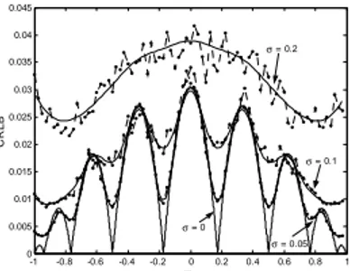
In this paper, the CRLB is analyzed assuming a zero mean Gaussian noise superimposed to the ADC input sinewave, which is a situation of more practical interest. In particular, Fig.1 shows how the CRLB for unbiased estimators depends on the transition level T0 of a single bit A/D. Both simulation and theoretical results achieved for various noise levels
are reported in this figure. Simulation results are obtained by applying Monte Carlo methods for the estimation of the partial derivatives required by the Fisher information matrix [6][7][8]. In particular, 107 data records each based on M=9
samples of a full-scale sinewave have been used. Conversely, the theoretical results have been obtained by numerically
integrating (B.7) and (B.11) reported in Appendix B, which can not be easily solved analytically. It can be seen that simulation data show a good agreement with theoretical results. Moreover, the CRLB has a more regular behavior with respect to the pure sinewave case, varying less abruptly with the threshold when additive Gaussian noise is present. This can be explained by observing that the CRLB changes are due to the lack of knowledge about the phase of the input sinewave, whose effect tends to become negligible when the noise level increases [2]. It is worth noticing that for moderate amounts of noise, the CRLB maxima are lower than the corresponding ones when a noiseless sinewave is assumed, while under the same assumptions the CRLB minima are higher.
Since (1) is a biased estimator [5], the results reported in Fig.1 require adjustments in order to provide the corresponding CRLB. Figs. 2(a) and 2(b), show the variance σT2k of (1) (given by (8)), the related noise contribution, and the CRLB associated to biased estimators (see appendix B), obtained for two different noise levels. These results have been obtained by considering an overdrive voltage VOD = 0.3FS. In fact, the Cramér-Rao bound increases very
Fig. 1: CRLB, simulation and theoretical results, plotted as a function of the value
assumed by the transition level T0. The continuous lines have been obtained
theoretically, while the dotted lines report simulation results.
-1 -0.8 -0.6 -0.4 -0.2 0 0.2 0.4 0.6 0.8 1 0 0.005 0.01 0.015 0.02 0.025 0.03 0.035 0.04 0.045 T 0 CR L B σ = 0.1 σ = 0.2 σ = 0.05 σ = 0
quickly when transition levels close to the input sinewave amplitude are estimated. Notice that σT2k presents local minima, which coincide with the CRLB when the threshold level T0 is not close to the sinewave amplitude. Thus, the
SHT is locally optimal with respect to the statistical efficiency. Also notice that (8) is the summation of two positive terms. The first one is due to lack of knowledge about the sinewave phase and is responsible for the oscillations of σT2k , while the second one models the noise contribution. Since the local minima of (8) correspond to values of T0 where first
term is null, Fig.2 shows that the second term of (8) is very close to the CRLB. Now, for large values of M, the effect of sinewave phase behaves like 1/M2, while the noise contribution tends to zero like 1/M. Hence, for values of M used in
practice, it is expected that the SHT provides almost efficient estimators also for noisy input signals. Furthermore the CRLB associated to the transition level estimators can be expressed as
1 ,.., 0 , , 78 . 1 2− 2 ≥ = − ≅ A T A T k N M CRLB σ k k (14) IV. EXAMPLE
To illustrate the use of the procedure described in section II, we performed a SHT on a National Instruments 6023E 12-bit data acquisition board (DAQ). On preparing the test we assumed the following requirements were made: “Test the dynamic performance of this DAQ at its maximum sampling frequency and in the ±10V range using the SHT”. Since we are testing a 12-bit ADC we need a sinusoidal function generator with a SFDR better than 74dB as mentioned before and which can output amplitudes a little higher than 10V (the DAQ full-scale). Thus we used the Stanford DS360 Function Generator. We chose here to perform the test with a 200Hz sinusoidal stimulus signal. A more complete approach would require the repetition of the test for different input frequencies in order to transmit to the end-user the behavior of this particular board in different input signal conditions. Since the specifications for the function generator do not supply information about the SFDR but only about the total harmonic distortion (THD) [2], which is stated to be better than 105dB, we will assume that the SFDR will be better than the required 74dB.
-1 -0.8 -0.6 -0.4 -0.2 0 0.2 0.4 0.6 0.8 1 0.03 0.04 0.05 0.06 0.07 0.08 0.09 0.1 0.11 T 0 CRLB (a) σ2 Tk σ2 Tk square root term
Fig. 2: Variance of the SHT estimates and CRLB, evaluated for biased estimators, σ=0.2 (a) and
σ=0.05 (b). The square root term of (10) is also plotted.
-1 -0.8 -0.6 -0.4 -0.2 0 0.2 0.4 0.6 0.8 1 0 0.01 0.02 0.03 0.04 0.05 0.06 0.07 T 0 σ2 Tk CRLB σ2 Tk square root term
For the determination of the exact amplitude of the sinusoid to use we will assume a maximum possible gain error,
εG, of 2.75% and a maximum possible offset error, eD, of 28mV according to the DAQ specifications. Using (3) this
leads to an input range, V’r, of 20.62V.
To determine the required overdrive the standard deviation of additive noise must be known. The DAQ specifications state a value of 0.1 LSB for the “system noise not including quantization.” The test setup however also contributes to the additive noise. We performed a test using the method recommended in [2] and estimated the total additive noise to have a standard deviation of 2mV. The function generator amplitude error was stated has being 1%. In our case where the sinusoid amplitude is close to 10V this corresponds to a possible amplitude error of 100mV (eA). The amplitude
resolution is stated to be “4 digits or 1µV whichever is greater.” In our case this corresponds to 10mV (rA). The sinusoid
amplitude chosen was A=10.42V according to (4), and considering BeINL=0.1LSB and BεDNL=10%.
The minimum number of samples has been calculated, obtaining 1,684,607 for a precision in the INL and DNL values of BpINL =0.1LSB and BpDNL=0.2LSB. In order to guarantee (2) and using the procedure suggested in [2] we
reached the value of 1,684,999 for the number of acquired samples and an input frequency of 200 Hz (J=1685). Furthermore, the standard uncertainties σINL and σDNL have been evaluated according to [10], obtaining σINL=0.06LSB
and σDNL=0.016LSB. Such results are compatible with the INL and DNL precisions.
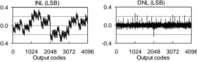
The test was executed and the independently based gain and offset errors were computed according to [2] leading to the values 0.14% and -2.82mV respectively. These values are lower than the maximum values chosen a priori (2.75% and 28mV) so those assumptions were verified. The estimated INL and DNL, computed from (11) and (12), are represented in Fig. 3. INL (LSB) -0.4 0.0 0.4 0 1024 2048 3072 4096 Output codes DNL (LSB) -0.4 0.0 0.4 0 1024 2048 3072 4096 Output codes
Fig. 3: Representation of the estimated INL and DNL sequences.
V. CONCLUSIONS
The performances and the efficiency of the SHT, have been discussed and analyzed in this paper. In particular, the characterization of the test performance has been improved by removing some commonly adopted approximations. Finally the statistical efficiency of the SHT has been evaluated by comparing the estimator variance to the corresponding CRLB, computed both theoretically and by means of simulations. The results suggest that the SHT is asymptotically optimal also when a Gaussian white noise is superimposed to the sinusoidal stimulus.
VI. APPENDIX A: DERIVATION OF THE CONSIDERED OVERDRIVE
In [4] the sampled voltage amplitude distribution is computed by convolving the amplitude distribution of a perfect sinusoidal signal with the probability density function of Gaussian noise (see (31) in [4]). The probability distribution of the estimated transition voltages is then approximated using a Taylor expansion leading, after some simplification, to (33) of [4]. The overdrive is then determined so that the maximum error for the INL is less than B/4 LSBs where B is specified by the user:
QB
VODINL =σ2 . (15)
Because of the approximations used, the actual error is 28% greater then B/4 when using VODINL given by (15) for values of VODINL lower than 2σ [4], expression (15) was changed to
= QB VODINL 2 , 2 max σ σ , (16)
which is the expression (9) proposed in [4] and also used in Eq. (10) of [2]. Here we suggest three changes to it, leading to Eq. (6):
• Instead of defining the maximum admissible error for the INL has a fraction of ¼ LSB (B) we define it as a fraction of 1 LSB (BeINL). So BeINL=B/4;
• We calculated numerically the actual INL error for a wider range of values of the additive noise standard deviation than those calculated in [4] and found that it is in the worst case 28% higher than the value given by the approximation leading to (15) for any value of VODINL, not just for values higher than 2σ as stated in [4]. So we propose that the factor 2σ is removed from (16) and a multiplying factor 1.28 is used as shown in (6);
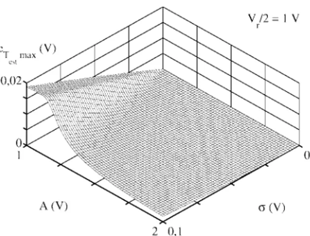
• In Fig. 4 we represent the results of the numerical calculation of the transition voltage estimation error. It is observed that the error is always lower than σ /5 for σ lower than 1% of the sinusoid amplitude (A). As a consequence we would limit the usage of overdrive to the situation when the maximum admissible error is lower than one fifth than the noise standard deviation. For higher values of maximum admissible error (BeINL) there is no need to use overdrive because the error will never be greater than BeINL as shown in Fig. 4
Fig. 4: Representation of the maximum estimated transition voltages error as a function of sinusoid amplitude and noise standard deviation determined by numerical integration of the analytical expressions for the error.
The proposed expression for the amount of overdrive required to guarantee an error in the estimated values of the INL lower than BeINL is thus (6).
In the case of the error in the code bin widths (and DNL), [4] starts by calculating the probability density of the sampled signal by convolving the probability density of a sinusoid with the probability density of Gaussian noise [4]. Then the ratio between the estimated code bin width Wˆ and the real code bin width W is approximated by the ratio between the probability density of the sampled voltage when additive noise is present (g(x)) and when it is not (f(x)) as stated in the equation following Eq. (27) in [4]. This is just approximately true because the proportionality constant between Wm and g(x) is different from the probability constant between W and f(x). Blair then proceeds to determine the
relative error and then the amount of overdrive required, obtaining the following expression 3 2 DNL OD V B σ = . (17)
Because of the approximations used, the actual error is 43% greater then B when using VODDNL given by (17) for values of VODDNL lower than 3σ, so expression was changed to
3 max 3 , 2 DNL OD V B σ σ = , (18)
which is present in Eq. (8) of [4] and which is also used in [2].
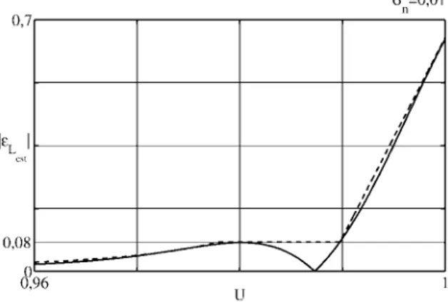
Here the relative error εLest of the code bin widths estimation was computed numerically (solid line in Fig. 5) and an
empirical expression was determined in order to a make it possible to compute approximately the relative error (dashed line in Fig. 5). This lead to expression (7) for the amount of overdrive required to guarantee a relative error lower than
Fig. 5: Representation (solid line) of the relative error of the estimated code bin widths as a function of the transition voltage divided by the sinusoid amplitude (for null offset), U, for a noise standard deviation equal to 1% of the sinusoid amplitude. This was determined using numerical simulation. The dashed line represents the approximation given by (7).
VII. APPENDIX B: DERIVATION OF THE CRLB FOR SINEWAVE ADC INPUT AFFECTED BY ADDITIVE GAUSSIAN NOISE
Let us indicate with T the vector of the ADC transition levels to be estimated, and let us define Y as a random variable (rv) whose possible realizations belong to the space of the experimental outcomes. Furthermore, let us assume that tT is a scalar statistic of the sample space associated to the ADC output, expressed as a function of the unknown
ADC transition levels. The CRLB associated to the variance of an estimator t’ of tT with a bias bT = E[t’]-tT is given by
[
]
[
T T]
T T T b F t b t CRLB= ∇ +∇ −1∇ +∇ , (B.1)where ∇ is the gradient operator, that is ∇tT=[∂tT/∂T0, ∂ tT/∂T1,…, ∂tT/∂TN-1], and ∇bT =[∂bT/∂T0, ∂bT/∂T1,…, ∂bT/∂TN-1]
[5]. As this analysis is focused on the CRLB associated to the estimation of the i-th transition level Ti, we have tT =Ti
and: ≠ = = ∂ ∂ j i j i T t j T , 0 , 1 , (B.2)
Let us define P{Y=Y;T} as the probability of occurrence of a given realization Y in the sample space of the ADC output. The Fisher information matrix can be expressed as [7]:
{
}
[
]
[
{
}
]
{
P Y T P Y T T}
E
F = ∇log Y= ; ∇log Y= ; , (B.3)
where E{·} is the expected value operator. By developing (B.3), the elements of the Fisher information matrix may be obtained as
{
}
{
} {
}
∑
= ∂ ∂= ∂ ∂= = Y m n m n P Y T P TY T P T Y T F ; ; ; 1 , Y Y Y , (B.4)In the following subsections, the CRLB on the estimation of the ADC transition level will be discussed for an ADC stimulus consisting of a sine-wave corrupted by additive white Gaussian noise. Both unbiased and biased estimators will be considered.
a) Unbiased estimators
Let us assume that the ADC stimulus is expressed by the following 1 ,..., 0 , 2 sin + = − + = n n M M D A xn π φ ηn , (B.5)
where M is the record length, D and M are mutually prime numbers, φ is the initial phase, which is uniformly distributed in [0,2π] when different records are considered, and ηn is a zero mean Gaussian white noise with standard deviation σ.
Let us define X=[x0…xM-1] as the vector of random variables that models the samples at the ADC input. Similarly, let
us define Y=[y0…yM-1] as the vector of the corresponding ADC output codes. If N is the number of ADC thresholds and
N+1 the number of output codes, Y may assume (N+1)M different values. In a single record of M samples, φ is constant,
so the ADC input (B.5) is a sequence of normally distributed and mutually independent random variables, with mean values E{xn} = Asin(2πDn/M+φ). Hence, by noticing that the ADC transfer function is memoryless, the probability of
occurrence of a given ADC output sequence is given by the product of the marginal probabilities of occurrence of the individual samples, that is:
{
}
{
{
}
}
∫
∏
− = = = = = π φ φ π φ 2 0 1 0 ) ; | ( 2 1 ; | ; M j i j y T d P T Y P E T Y PY Y . (B.7)where Pj{yi|φ ;T} is the probability that the j-th sample of the ADC output equals a given output code yi, conditioned to
the values assumed by the initial phase φ, and the outermost expectation is carried out over φ. This operation, performed by integrating on the real axis the product of the marginal probabilities Pj{yi|φ ;T} and the phase probability density
function, removes the dependence on φ. By observing that Pj{yi|φ ;T}=P{Ti-1≤yj<Ti}, the marginal probabilities can be
= + − Φ − − = + − Φ − + − Φ = + − Φ = − − N i M Dj A T N i M Dj A T M Dj A T i M Dj A T T y P N i i i j σ φ π σ φ π σ φ π σ φ π φ 2 sin 1 1 ,..., 1 2 sin 2 sin 0 2 sin ) ; | ( 1 1 0 , (B.8)
where Φ(⋅) is the probability distribution function of a zero mean unity-variance Gaussian rv.
In order to derive the Fisher matrix, the partial derivatives of P(Y=Y;T) with respect to the transitions levels Ti are
needed. To this extent, it can be observed that Pj(yi|φ,T) is differentiable with respect to any Ti. Hence, according to
theorem 4.1 in [11] it is possible to differentiate under the integral sign, as expressed by the following
{
}
∫
∏
{
}
∫
∏
−{
}
= − = = = = π π φ φ π φ φ π 2 0 1 0 2 0 1 0 ; | 2 1 ; | 2 1 ; M j i j h M j i j h h d T y P dT d d T y P dT d T Y P dT d Y , (B.9)where the derivative of the product of the marginal probabilities can be rewritten as
{
}
∑
{
}
∏
{
}
∏
− = ≠ − = = 1 0 1 0 ; | ; | ; | M j k j i k i j h M j i j h T y P T y P dT d T y P dT d φ φ φ , (B.10)By applying (B.8), the derivatives of the marginal probabilities are expressed by
− = = + − − = − = + − = otherwise i h N i j M D A T i h N i j M D A T T y P dT d i i i j h , 0 1 , ,... 1 , 2 sin 1 , 1 ,..., 0 , 2 sin 1 ) ; | ( ϕ π φ σ σ σ φ π ϕ σ φ , (B.11)
where ϕ(⋅) is the pdf of a Gaussian zero mean unity-variance rv. Finally, equations (B.4), (B.7) and (B.11) provide the Fisher information matrix and the CRLB for unbiased estimators.
b) Biased Estimators
When biased estimators are considered, the CRLB depends on how the bias varies with the ADC transition levels. In particular, for SHT estimators we have [3]:
{ }
, , 0,..., 1 2 ' 2 2 2 − = − = − = − = T T C k N T A T t t E b k k k k Tk k Tk σ , (B.12)where bTk is the k-th element of bT, that is the bias of the k-th ADC transition level estimator. It follows that the partial
derivatives of bT are given by
≠ = − + = ∂ ∂ j i j i T A T A T b i i j Ti , 0 , 2 2 2 2 2 2 2 σ (B.13)
In particular, when a single bit ADC is considered , from (B.4) we have:
1 2 2 2 0 2 2 0 2 2 2 1 − − + + = F T A T A CRLB σ , (B14) ACKNOWLEDGMENTS
This work was partially sponsored by the Portuguese national research project entitled “New measurement methods in Analog to Digital Converters testing” (ref. PCTI/ESE/32698/1999), and by the Italian national research project entitled “Procedures for the characterization of analog to digital conversion apparata in large-scale and complex measurement systems” (ref. MURST/2001091873_005), whose support the authors gratefully acknowledges.
REFERENCES
[1] P. D. Capofreddi, B. A. Wooley, “The Use of Linear Models in A/D Converter Testing,” IEEE Trans. on
Circuits and Systems-I, Vol. 44, No. 12, Dec. 1997, pp. 1105-1113.
[2] IEEE Std 1057-1994, “IEEE Standard for digitizing waveform recorders”.
[3] IEEE Std. 1241-2000, “IEEE Standard for terminology and test methods for analog to digital converters ” [4] J. Blair, "Histogram measurement of ADC nonlinearities using sine waves," IEEE Trans. on Instrumentation
and Measurement, Vol. 43, No. 3, June 1994, pp. 373-383.
[5] P. Carbone and D.Petri, “Noise Sensitivity of the ADC Histogram Test,” IEEE Trans. on Instrumentation
and Measurement, Vol. 473, No 4, June 1998, pp. 1001-1004.
[6] P. Carbone, E. Nunzi, D. Petri, “Efficiency of ADC Linearity Estimators,” IEEE Trans. on Instrumentation
and Measurement, Vol. 51, No. 4, Aug. 2002, pp. 849-852
[7] G. Ivchenko, Y. Medvedev, Mathematical Statistics, Mir Publishers Moscow, 1990. [8] S. M. Kay, Modern Spectral Estimation, Prentice Hall, 1988
[9] A. O. Hero, J. A. Fessler, M. Usman, “Exploring Estimator Bias-Variance Tradeoffs Using the Uniform CR Bound,” IEEE Trans. on Signal Processing, Vol. 44, No. 8, Aug. 1996, pp. 2026-2041.
[10] ENV13005, “Guide to the Expression of Uncertainty in Measurements” [11] S. Lang, Calculus of Several Variables, Third. Ed., Springer-Verlag, New York.