Alma Mater Studiorum · Universit`
a di Bologna
Scuola di Scienze
Corso di Laurea Magistrale in Fisica
Thermally reduced Graphene Oxide:
a well promising way to transparent flexible
electrodes.
Relatore:
Prof. Beatrice Fraboni
Correlatore:
Prof. Paolo Samor`ı
Presentata da:
Serena Morselli
Sessione III
Contents
Abstract iii
Introduction v
1 Theoretical 2
1.1 Graphene: history, properties and perspectives . . . 2
1.2 Processability limits of graphene and advantages of graphene oxide . . . 4
1.3 Reduction methods . . . 6
1.4 Transparent conductive films (TCFs) . . . 8
1.5 Flexible electronics . . . 9
2 Materials, methods and instruments 12 2.1 Graphene Oxide . . . 12 2.2 Rhodamine 6G . . . 13 2.3 Deposition technique . . . 14 2.4 Annealing process . . . 15 2.5 Device fabrication . . . 17 2.6 Film transfer . . . 18
2.7 Atomic Force Microscopy . . . 19
2.7.1 Contact mode AFM . . . 20
2.7.2 Tapping mode AFM . . . 21
2.7.3 Force spectroscopy . . . 22
2.7.4 AFM tips . . . 23
2.8 X-rays Photoelectron Spectroscopy . . . 24
2.9 Electrical characterization . . . 27
2.9.1 Sheet resistance . . . 28
2.9.2 Gating effect . . . 29
2.10 UV-vis-NIR transmittance measurements . . . 29
2.11 UV-photoelectron spectroscopy . . . 31
2.12 ThermoGravimetric Analysis . . . 33 ii
CONTENTS iii
3 Experimental 36
3.1 Film morphology through AFM characterization . . . 36
3.2 XPS analysis . . . 40
3.3 Sheet resistance . . . 42
3.4 Transmittance . . . 44
3.5 ThermoGravimetric Analysis . . . 46
3.6 UPS data analysis . . . 47
3.7 Electrical characterization . . . 49
3.8 Rhodamine 6G doping . . . 51
3.9 Mechanical characterization . . . 53
Conclusions 58
Abstract
La presente tesi studia la riduzione termica dell’ossido di grafene nell’ottica di una ot-timizzazione del processo in termini di conducibilit`a elettrica e trasmittanza ottica, con lo scopo di ottenere parametri favorevoli alla creazione di elettrodi trasparenti e flessibili. La riduzione termica `e uno dei possibili metodi per ripristinare le propriet`a elet-triche originarie del grafene, compromesse dalla presenza dei gruppi ossidanti, i quali rompono i doppi legami C-C del reticolo a celle esagonali, ma in compenso rendono il materiale altamente idrofilo e trattabile in soluzione. Questo consente la deposizione di film di ossido di grafene tramite spin-coating, tecnica ottimale per la produzione di film uniformi e di spessore controllabile e riproducibile, e la successiva riduzione termica, ef-fettuata variando i parametri chiave, ovvero temperatura e tempo di riduzione e velocit`a di riscaldamento, con l’obiettivo di ottimizzare il processo.
Il presente lavoro si compone di un capitolo introduttivo volto a presentare la storia del grafene, dalla sua scoperta alle prospettive applicative future, tra cui l’elettronica trasparente e flessibile, con un particolare focus sull’ossido di grafene come punto di partenza per garantire scalabilit`a industriale ed economicit`a del processo. A seguire, un capitolo su materiali, metodi e tecniche traccia una panoramica sui differenti set up sperimentali per la produzione dei campioni, la loro manipolazione e, in particolare, gli apparati utilizzati per effettuare la loro caratterizzazione, che sfrutta tecniche quali microscopia a forza atomica, spettroscopia UV e a raggi X, analisi termo-gravimetrica, spettrofotometria UV-vis-NIR. I dati ottenuti da queste misure sono, infine, presentati e discussi nel terzo capitolo, incentrato sugli aspetti sperimentali.
I risultati raggiunti sono promettenti. La deposizione via spin-coating produce film continui e uniformi in rugosit`a e spessore. Il processo di riduzione `e stato ottimizzato in termini di sheet resistance e trasmittanza ottica, raggiungendo valori pari a, rispettiva-mente, (19±1)kΩ/2 e 82,9% a 550nm per un campione di pochi nanometri di spessore, a significare buona conduttivit`a combinata con ottima trasparenza sull’intero range UV-vis-NIR. Questi risultati sono la conclusione di un processo di selezione di temperature e tempi di riduzione, oltre che di perfezionamento della fase di riscaldamento del campi-one, che si `e avvalso di analisi XPS e termogravimetriche, oltre a misure di trasmittanza ottica e sheet resistance tramite metodo a quattro punte.
In termini di funzione lavoro, i film di grafen ossido ridotto termicamente mostrano iv
ABSTRACT v una work function variabile a seconda del grado di riduzione, consentendo di spaziare su valori compresi tra i 5.0eV e i 5.4eV, con un trend orientato verso i valori del grafene per i film maggiormente ridotti. Questo dato `e positivo perch´e, nel caso di integrazione del film in dispositivi richiedenti una specifica work function, si ha modo di selezionare quella pi`u adeguata.
Per quanto riguarda l’estensiva caratterizzazione elettrica dei film sotto effetto di gate, si evince dalle curve IdVg un alto numero di difetti reticolari, i quali si traducono in
mobilit`a ridotte per entrambi i portatori di carica e in uno shift positivo del Dirac gate voltage, punto in cui i portatori di carica passano da essere elettroni a lacune e viceversa, atteso a 0V. Effettuando, per`o, un drogaggio tramite Rodamina 6G, noto dopante di tipo n per il grafene, si ottiene un interessante shift negativo della curva, che porta il Dirac point a circa 10V e che pu`o essere ulteriormente diminuito di 20V irradiando il campione alla frequenza di assorbimento della Rodamina 6G, in modo da indurre il trasferimento elettronico dalla Rodamina al film di grafen ossido ridotto. Questo trasferimento elettronico `e alla base del meccanismo con cui il film effettua quenching della fluorescenza della Rodamina ed `e reversibile solo mediante prolungato passaggio di corrente nel film. In sostanza, mostriamo come il drogaggio del film tramite Rodamina 6G si componga di due fasi successive, una per semplice deposizione, l’altra innescata dall’irradiazione, entrambe reversibili e di tipo n.
Infine, grazie al fatto di aver messo a punto una tecnica di trasferimento del film su substrati altrimenti inadatti perch´e patternati o non riscaldabili alle alte temperature della riduzione (come il PET), abbiamo potuto misurare le curve di carico del film sospeso su una micro-well tramite AFM e estrarre il modulo elastico 2D di pochi layers di grafen ossido ridotto, ottenendo valori dell’ordine di 103 N/m, superiori a quelli del grafene.
Introduction
The carbon atom is a fundamental building block in nature; the complexity of its chemical bonds is the main reason of its being at the origin of life. According to its degree of hybridization (sp, sp2, and sp3), it can assembly into different materials. Some of them
have been known for a long time, such as natural graphite and diamond, but, particularly in the last half century, the researchers have uncovered many new materials. Graphite has been the first to be object of intense studies, after the identification of its structure in the beginning of the 20th century, and it followed a development of both theoretical and experimental aspects. In 1985, the discovery of fullerene started the era of nanocarbons, which, in the following years, included also nanotubes and graphene. In particular, the attention of the scientific world is now on graphene thanks to Geim and Novoselov of Manchester University, whose work presenting the isolation of monolayer graphene in 2004 and winning the Nobel Prize in Physics in 2010 can be considered the key event for the actual scientific and technological interest in graphene and graphene based materials. Graphene, a two dimensional honeycomb lattice of carbon atoms, is known for its excellent electrical and mechanical properties, its thermal stability and for the particular feature of being a zero band gap semiconductor, with switchable charge carriers and very high mobility. Graphene has therefore an enormous potential in technological applica-tions and the involved field can be several: from high frequency electronics to chemical sensors, touch panels, conductive ink, energy, and light emitting devices. The creation of new technologies based on graphene is subject to overcoming a variety of challenges and achieving several goals. Among these, the production of graphene is a very important aspect: we need to find reproducible, reliable, safe and sustainable large-scale production methods for graphene and related materials, according to the specific needs of different application areas.
The possible techniques for graphene production are many, from mechanical exfolia-tion of highly oriented pyrolitic graphite, to substrate based processes (epitaxial growth and chemical vapor deposition). One of the most promising path for a highly scalable, inexpensive production method is the reduction of the graphene oxide (GO) obtained by oxidation and exfoliation of graphite.
The present work is focused on the reduction of graphene oxide via thermal annealing, one of the several ways to perform the reduction. Thermal reduction is far more health
INTRODUCTION 1 and environmental safe than chemical reduction, because of the negligible side products. Moreover, thermal reduction gives the possibility to deal with graphene oxide in solution and reduce it after deposition. In fact, GO is highly dispersible in water because of the oxidizing groups, so that we can work with solutions instead of powders or isolated flakes for what concerns the formation of the film, and we proceed with the reduction only after the deposition. Depositing solutions is an optimal starting point to have uniform films of controllable thickness.
Our aim is to optimize the reduction process to obtain films that are not only con-ductive, but also transparent. For a set thickness, we can play with annealing time and temperature, and vary the heating ramp, so that optical transmittance and sheet resistance are optimized.
More in detail, after a theoretical introduction in Chapter 1, where the history of graphene, its declination as graphene oxide and relative advantages, and some perspec-tives concerning its applications in flexible electronics are presented, in Chapter 2 we illustrate the materials, the instrument we use, and the production techniques we follow. In particular we produce reduced graphene oxide (rGO) films on quartz for transmit-tance and sheet resistransmit-tance measurements and on Si/SiO2substrates to build bottom-gate,
top-contact field-effect transistors for electrical characterization under gate bias. We also optimize a transfer technique that enables the deposition of reduced films even on flexible substrates.
In Chapter 3 we illustrate the measurements we perform on the samples and we analyze the results. In particular, we characterize the rGO film morphologically via AFM and we examine the thickness of the film before and after reduction in search of a correlation between the two values. Thanks to sheet resistance and XPS spectra, we check the degree of reduction of the film and select the most promising range of reduction temperatures in terms of conductivity. The optical transmittance values, instead, are the key parameter to restrict the range of possible reduction times and give the start to an analysis of the influence of the heating ramp on the thinning of the film during reduction, mastered with ThermoGravimetric Analysis. From the UV-photoelectron spectroscopy data, we are able to individuate a trend of the rGO work function, according to the degree of reduction. Afterwards, we perform the electrical characterization of field-effect transistors, which gives indications on the quantity of defects in the lattice and is useful to analyze the doping effect of Rhodamine 6G on rGO films and the fluorescence quenching of the dye by the graphene. Finally, the transfer of the reduced films on patterned substrates allows us to measure the Young modulus of our film, using an Atomic Force Microscopy technique on rGO membranes suspended over micrometric wells.
Chapter 1
Theoretical
1.1
Graphene: history, properties and perspectives
Reduced graphene oxide (rGO), the material on which this work is focused on, is a graphene derivative resulting from the attempt of enhancing the processability and the large-scale production of graphene itself. In few pages, it will be clear why the choice of the material ended up on rGO, but in order to have a better understanding of its structure, properties, and the goals connected with the reduction process, it is important to introduce first its precursor the graphene.
Graphene is a structure made by sp2-hybridized carbon atoms arranged into a
two-dimensional sheet following a hexagonal lattice, the so-called honeycomb lattice. The stack of multiple graphene layers, hold together by Van der Waals interaction, gives rise to 3D graphite, while the roll up of a single flakes originates 1D carbon nanotubes and if the honeycomb lattice is arranged to form a spherical particle, we have 0D fullerene. The interest in graphene is due to the extraordinary thermal, electrical and mechanical properties that this carbon allotrope presents. The expectation of the theoretical studies have been confirmed in 2004 by Geim and Novoselov’s work1 that presented isolated single graphene flakes, confuting the hypothesis that such bi-dimensional crystals were thermodynamically stable only at infinitesimal temperatures.
The anisotropic structure of graphitic materials leads to interesting anisotropic prop-erties. In particular, the s, px and py orbitals of each carbon atom are hybridized,
forming covalent sp2 bond that appear at 120◦. Out of plane, instead, the remaining p z
orbital, together with the three neighbor atoms, form a valence band of π orbitals and a conduction band of π* orbitals. The four electrons of each carbon atom contribute to form in-plane bonds (three electrons are employed for the σ bond and one for the π bond), therefore there are no more electrons to develop further chemical bonding in the c-direction. The out-of-plane interactions are then very weak, resulting in very low thermal and electrical conductivity in c-direction, three order of magnitude smaller than
CHAPTER 1. THEORETICAL 3
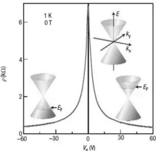
Figure 1.1: Graphene band structure with and without gating, and the consequent am-bipolar electric field effect on the carriers. At zero voltage, valence and conduction band spontaneously meet at the single Dirac point. When a positive (negative) gate is applied, electrons (holes) are injected, inducing an enhancement of their mobility as result of the shift of the Fermi level (EF).3
their in-plane analogous2. Because of this orbital structure, graphene flakes composed by few carbon layers show a metallic behavior, since some carrier wave functions over-lap; the single-layer graphene flakes, instead, behave quite differently and are classified as zero band gap semiconductors (or semimetal). They present, in fact, a single Dirac point, which is the intersection of the highest occupied molecular orbital (HOMO) and the lowest occupied one (LUMO) (see Figure 1.1).
The main consequence of this electronic structure is ambipolarity: gating the graphene, the Fermi level, normally coincident with the Dirac point, can be shifted in the valence or conductive band, that is to say the carriers can be continuously tuned between holes and electrons, according to the gate applied. For non-zero gate, the electrical resistivity drops and the carriers gain a very high mobility up to 200000 cm2V−1s−1 (single-layer,
mechanically exfoliated, suspended graphene flake).3 These high mobility values are due
to the surprisingly low density of defects that normally inhibit charge transport, acting as scattering centers.4
The potential of development and engineering of this material is enormous and the idea of a new electronic is very tempting: by simply gating the graphene, doping levels become dynamically controllable and completely reversible, and the device can be easily reconfigured without any physical modification. Ambipolarity is an advantage also for the application of graphene as sensor. 2D materials are already a very favorable choice
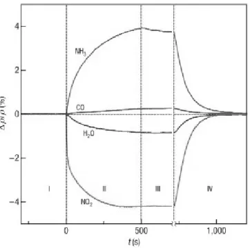
CHAPTER 1. THEORETICAL 4 for sensing processes because of their maximal area to volume ratio: in layered materials, where there is no distinction between surface and bulk, every adsorption event on the surface affects as well the properties that are classified as bulk ones (such as resistivity). This is typical of bidimensional materials, and in graphene it is enriched by ambipolarity, thanks to which the adsorption of either electron-donating or withdrawing groups is possible and meaningful.5 (See Figure 1.2)
Figure 1.2: Sensitivity of graphene to chemical doping. Changes in resistivity, ρ, at zero B caused by graphene’s exposure to various gases diluted in concentration to 1 p.p.m. The positive (negative) sign of changes is chosen here to indicate electron (hole) doping.5
1.2
Processability limits of graphene and advantages
of graphene oxide
The fundamental premise for these extraordinary applications and results is the produc-tion of single-layer graphene. The methods are many and have been wisely improved, but any of them should possibly respond to three important requirements: the process should ensure fine control over the crystallite thickness, it should produce films with low density of defects to have high carrier mobility, and it should be industrially scalable.
The first successful approach to single-layer graphene production has been the mi-cromechanical exfoliation method carried on by the Manchester group led by Geim.1The
CHAPTER 1. THEORETICAL 5 process to detach graphene from a graphite crystal (HOPG) consists in using adhesive tape, that at the first step removes multiple-layer graphene. To obtain few- or single-layer graphene, a repeated peeling is necessary, that also cleaves the graphene in flakes. Afterwards the tape is attached to the substrate and detached via glue solving. The last step is a peeling with an unused tape to further reduce the number of layers. Mechanical exfoliation is now optimized to yield high quality layers, with size up to the order of millimeters, limited only by the single crystal grains in the starting HOPG. Even if it is still the method of choice for fundamental studies, it is yet difficult to make it feasible for large-scale applications.
An alternative route that succeed in scalability is the graphene chemical vapor de-position (CVD) through hydrocarbons reacting with nickel or transition-metal-carbide surfaces. In fact the high temperature (over 1000◦C) of the Si/SiO2 substrate with a thin
layer (∼300nm) of nickel on it activates the adsorption of carbon on the substrate, and then the fast rate cooling to room temperature by argon flow suppresses the formation of multiple layers of graphene.6
Another substrate-based technique is the epitaxial growth, where silicon carbide is reduced at 1000◦C in UHV leaving behind graphitized carbon islands.7The substrate and
many growth parameters have a strong influence on the mechanical properties of the film grown with epitaxial growth or with CVD and for both of them, even if the scalability is potentially very good, the control of the thickness is still a difficult achievement.
To conclude this brief overview on the main production techniques of single-layer graphene, it is important to talk about the graphene oxide and its reduction. Graphene oxide is a graphene related material that presents the same layered, honeycomb-lattice structure and can be commercially found as a water dispersion. The main differences with the graphene are exactly its hydrophilicity, and the presence of many defects, as missing bonds inside the lattice or as oxygen-containing groups at the edges or in the basal plane, that inhibits charge transport and makes the GO flakes insulating. The origin of these extra groups bonded to the flake is their production method that start from oxidizing graphite. By Hummers method,8 in fact, an aggressive chemical reaction,
driven by a mixture of sulfuric acid, sodium nitrate and potassium permanganate, breaks the double carbon-carbon bonds of graphite and induces the intercalation of groups such as epoxy or hydroxyl ones between the layers. In this configuration, the layers of graphite are more spaced and easily separable (by sonication, stirring or thermal expansion for example) and the groups now decorating the single- or few-layers flakes make them much more hydrophilic. Their dispersion in pure water or aqueous mixture is easily achieved and this is of sure advantage to the formation of a thin film. Actually, many common techniques can be applied to deposit uniform and thickness-controlled films, such as spin coating, rod coating, spray coating, Langmuir-Blodgett technique, ink-jet printing, drop casting, dip casting and many others.9
CHAPTER 1. THEORETICAL 6
Figure 1.3: Structure of graphene oxide with epoxy and hydroxyl functional groups decorating the carbon plane and carboxylic groups on the periphery. Minor groups, as carbonyl, ester, etc. are omitted.10
1.3
Reduction methods
Graphene oxide is still a hot topic for what concerns the mass applications of graphene in particular and its development in general, even if the research has already elaborated few interesting methods for graphene production that guarantee excellent properties as a consequence of the relatively perfect structure of the products. Significant examples of these methods are epitaxial growth,11 12 13 micro-mechanical exfoliation of highly ordered
pyrolityc graphite1, and CVD (chemical vapor deposition),6 12 14 but in comparison to them, the GO methods still has two advantages for what concerns the aimed large-scale use of graphene: first, graphene oxide can be produced by inexpensive, high yield chemical methods that use as raw material cost-effective graphite; second, the high GO hydrophilicity allows to form stable aqueous colloids, facilitating the film formation processing the solution in cheap and simple ways. The graphene production process by GO is incomplete without the reduction step: the final product rGO presents restored conductive properties that depend upon the reduction process, which therefore affects the performances of the rGO-composed materials or devices. For this reason, the GO reduction is still a key topic that we will now investigate further.
The reduction processes for GO can be mainly classified in chemical methods, thermal methods or multistep ones, the latter including both chemical and thermal approaches. The chemical reduction, which is done in solution, is usually performed at room tem-perature or under moderate heating; therefore the equipment and the requirements for the environment are not as critical as in the thermal approaches. This makes gener-ally the chemical approach cheaper and easily available for rGO mass production. Not surprisingly, the most common reduction method, that has been also one of the first to be reported, is the GO chemical reduction by hydrazine monohydrate. Differently from many other reductans, hydrazine monohydrate and its derivatives do not react with
wa-CHAPTER 1. THEORETICAL 7 ter, making them very attractive for reducing aqueous dispersions of GO. Adding the reductant to the dispersion upon 80◦C to 100◦C heating, a black solid precipitates be-cause of the increased hydrophobicity of the material upon reduction. The black solid is in fact an agglomerate of graphene-based nanosheets that can be kept separated for an easy application by adding surfactants (soluble polymers) or ammonia. This method, very effective at removing oxygen functionality, has the relevant disadvantage of creating covalent bonds between nitrogen (in case of hydrazine and derivatives) and the graphene oxide surface. These residual C-N groups affect the electronic structure of the graphene, acting as n-type dopants.15
Other approaches that can be classified as chemical ones are Photo-catalytic reduc-tion, Electrochemical reduction and Solvothermal reduction.16
Looking for a reductant-free method that can avoid undesired doping of the material, the thermal approach is an interesting alternative for reduction. The thermal process can be performed both on liquid solution of GO and on solid, pre-deposited films of material. In liquid, the annealing of the GO solution allows to exfoliate and reduce the material at the same time. Actually, the pressure of the CO and CO2 gases evolved during the
reduction is enough to separate single sheets of material, leading directly to graphene as final product. The flakes obtained in this way are however very small and wrinkled, because the decomposition of oxygen-containing groups during the reduction also re-moves carbon atoms from the carbon plane, for a total mass loss of c.a 30% and a final structure heavily damaged,17 18 which affects the conductivity of the material. A partial
solution to this problem is to separate the exfoliation and the reduction steps: large sized GO flakes can be produced by liquid phase exfoliation of graphite, then brought to solid phase (e.g. film or powder) and finally thermally reduced. The reduction is carried out in vacuum,19 inert20 or reducing atmosphere,20 21 since residual oxygen has an etching effect on the material at high temperatures and the evolved gas can exert an exfoliating pressure on the film and a consequent loss of material. The choice between different atmospheres depends upon the set-up availability, the need of doping or not the material during the reduction and the maximal temperature available, since in case of H2 atmosphere the reduction can be carried out at lower temperatures. Of course, the
temperature is a key parameter for the good success of the thermal reduction, together with the heating speed and time. One of the indicators to classify the goodness of the reduction is the carbon-to-oxygen ratio (C/O ratio), obtained by XPS measurements or by elementary analysis measurements by combustion and goes from 4:1-2:1 in GO22 23 24 to values generally around 12:1 in rGO,24 25 but values of 246:1 have been recently
re-ported.26 For temperatures up to 500◦C, the carbon/oxygen ratio is hardly bigger than
8:1, indicating that the conversion of C=O and O=C-OH groups into new chemical species is still incomplete, but it improves significantly at higher temperatures (700◦C and 900◦C), where the C/O ratio is higher than 13:1.27 Obviously, thermal treatment is
energy and time consuming and the range of possible substrates for the film deposition is limited by the high melting point requirement, but still the thermal reduction is a
CHAPTER 1. THEORETICAL 8 highly effective method, far more healt-safe than the chemical one.
An interesting combination of chemical and thermal approaches is the multistep method, where, for example, a first exposition to hydrazine vapor reduces the annealing temperature required to complete the reduction of the material.28 This intuitively gives the possibility to use substrates with lower melting points, e.g. polymeric substrate, and the conductivity is comparable to that obtained for annealing at 550◦C, but still does not reach the highest values reported in literature.19 29
1.4
Transparent conductive films (TCFs)
The reduced Graphene Oxide is one of the transparent conductive films (TCFs) of the new generation, which are fundamental for many technologies, such as LEDs, solar cells, liquid crystal displays, sensors and many others, and are developing in the direction of a higher economic affordability for mass scale production. Apart from high electrical conductivity and low absorption coefficient in the visible light range, another general important requirement for TCFs is thermal stability. TCFs are often subjected to high temperatures because of thermoelectric effect and, in some application, direct exposition to natural heat (e.g. solar cells). Lastly, good etchability is a very desirable feature for TCFs because allows to form patterns in the electrode. Presenting all these features, In2O3/Sn Indium Tin Oxide (ITO), is the milestone of the TCFs market. More in
detail, it has high optical transmittance in the visible and near infrared region, higher than 80%,30 and very low sheet resistance, down to 6 Ω/2.31
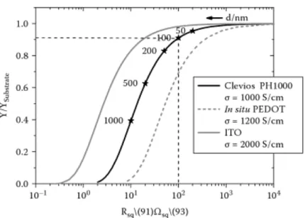
Due to the high costs of Indium, ITO is yet very expensive and many other materials are being investigated to find appropriate alternatives to it. An interesting alternative can be found among polymers: there are some conductive, organic polymers, which are also light weighted, inexpensive, flexible, and well compatible with plastic substrates. These polymers facilitate electron movement through their sp2 hybridized backbone and their optimization led to very competitive conductivity: the most common among these polymers is PEDOT:PSS (poly(3,4-ethylenedioxythiophene) polystyrene sulfonate) and its sheet resistance is comparable to that of ITO for the same value of relative optical transmission, as may be seen in Figure 1.4.
In this challenge for an optimal and less expensive alternative to ITO, graphene obtained via GO reduction is a very interesting competitor. As shown in Figure 1.5, the rGO presents high and stable transmittance values over a wide range of wavelengths, while, even if ITO and FTO have higher transmittance values at short wavelengths, they are yet strongly absorbing in near- and short-wavelength IR region. Apart from conductivity, that is object of optimization according to the different reduction methods, the rGO presents also: excellent mechanical properties;28the possibility to form a pattern
with laser reduction or by physical scratch; and, as shown later in this work: tunable work-function; morphological uniformity of the film; thermal stability; transferability
CHAPTER 1. THEORETICAL 9
Figure 1.4: Relative optical transmission of ITO, PEDOT:PSS and in situ PEDOT versus sheet resistance. For PEDOT:PSS the thickness of the film d(nm) is indicated with the asterisks.32
onto flexible substrates as a trick to avoid problems connected with the melting points of the desired substrates.
1.5
Flexible electronics
The field of flexible electronics is wide and constantly developing. Flexible can mean many things: elastic, non-breakable, bendable, lightweight, permanently shaped or roll-to-roll manufacturable. The first approach to flexible electronics dates back to the 1960s. Thinning single crystal silicon wafer cells to ∼100 µm, Crabb and Treble33and,
indepen-dently, Ray34made the first flexible solar cell arrays, in which the flexibility was given by the plastic substrate. In 1968, Brody and his team managed to assembly the first flexible thin film transistor (TFT).35After 1997, when poly-Si TFTs on plastic were reported,36 37
the flexible electronics became an hot topic and the research started to expand rapidly. Actually flexible electronic can lead to surgical and diagnostic implementation, natu-rally integrated with human body for an extremely innovative therapeutic perspective, or to wearable communication devices, or even, it can be the accelerator for the real-ization of the internet-of-things, thanks to energy self-standing sensors, and many other applications.
There are two approaches toward flexible electronics. The first profits by the ele-mentary mechanic result according to which the bending strain decreases linearly with
CHAPTER 1. THEORETICAL 10
Figure 1.5: Transmittance spectra of ITO (black), 10nm thick film of thermally reduced GO (dark grey), and FTO (light grey) as function of incident wavelength.29
thickness: this means that any material can be flexible, if you can make it thin enough. If a Si wafer is rigid and brittle, wires, nanoscale ribbons, or membranes of silicon are not and building up systems on elastomeric substrates where these flexible structures are shaped in a wavy form guarantees not only flexibility, but also stretchability and compressibility. (See Figure 1.6). The second approach relies on new materials, such as elastic conductors, that can be the constituents of flexible electrodes, active components of flexible devices or that can play the role of electrical interconnections between bend-able or even rigid devices.38Among these new materials, a key role is played by graphene,
for its unique electrical, mechanical and optical properties. The graphene properties can be complemented and enhanced by 2D crystals such as boron nitride (BN) and transition metal dichalcogenides (TMDs), just to cite the most promising two.39
For what concerns the fabrication techniques of the structures, the flexible electronic field can take advantage from the standard production methods. Indeed, in the transfer-and-bond approach is used a carrier substrate, like a glass plate or a Si wafer, on which the structure is fabricated and then transferred from there to a flexible substrate. Since the tools for microfabrication have been developed to work in plane, the transfer has to be done as late as possible in the process. The drawback of this approach is the limited surface coverage, together with the costs. A second approach, which yet cannot benefit of the standard fabrication technologies, consists in in loco fabrication of the electronics, directly on the flexible substrates. Apart from developing new process techniques and using new materials, direct fabrication requires relying on amorphous or polycrystalline
CHAPTER 1. THEORETICAL 11 semiconductors, which are suitable to be grown on foreign substrates, such as polymeric ones, that in turn cannot tolerate high temperatures; for this reason, in direct fabrication, it is imperative to strike a compromise between low-temperatures processes and device performances.40
Figure 1.6: Stretchable silicon circuit with a mesh design, wrapped onto a model of a fingertip.38
Chapter 2
Materials, methods and instruments
2.1
Graphene Oxide
The GO used for all the experiments is purchased from Graphenea. This is not a cost-oriented choice, since pure graphite has lower costs and the Hummer method itself is quite inexpensive. We want yet an evaluation of the reduction procedure without any further trouble derivable from the graphene oxide production, which has been already extensively studied.8 15 41 We purchase GO by Graphenea in water dispersion with a concentration of 4mg/ml, which undergoes stringent quality controls to ensure high quality and good reproducibility. In Table 2.1 we report the information on the GO properties given by the producer.
SEM and TEM images are furnished too, as well as elemental analysis through XPS (see Figure 2.1), where the analyzed sample consists in 2g of 4wt% GO in water, dried under vacuum at 60◦C overnight. The data of the elemental analysis are reported in Table 2.2.
Form Dispersion of graphene oxide sheets Sheet dimension Variable
Color Yellow-brown Odor Odorless Dispersibility Polar solvents
Solvents Water Concentration 4 mg/mL Monolayer content (measured in 0.5mg/mL) >95%*
Table 2.1: Properties of Graphenea Graphene Oxide as given by the supplier.42
(*) 4mg/ml concentration tends to agglomerate the GO flakes and dilution followed by slight sonication is required in order to obtain a higher percentage of monolayer flakes.
CHAPTER 2. MATERIALS, METHODS AND INSTRUMENTS 13 Carbon 49-56% Hydrogen 0-1% Nitrogen 0-1% Sulfur 0-2% Oxygen 41-50%
Table 2.2: Elemental analysis of a Graphenea GO sample of 2g 4wt% dried. Correspon-dent XPS graph reported in Figure 2.1.42
Figure 2.1: SEM, TEM and XPS data of 2g 4wt% dried GO of Graphenea.42
The product is stable at room temperature and we keep it in the original bottle, sealed with Parafilm M to avoid unwanted change in concentration, or in vials with lower capacity for easiness of usage. We pay particular attention, every time we open the bottle, to be far from any heat or humidity source, not to modify the dispersion concentration by water condensation or evaporation.
2.2
Rhodamine 6G
Rhodamine 6G (or Rhodamine 590) is a dye, whose molecular structure is shown in Figure 2.2. It is by far the most used dye for fluorescence tracing and lasing medium.43
It is safe to use (it is harmful only if swallowed) and commercially available. We use Rhodamine 6G purchased by Sigma Aldrich with Dye content ∼95%. In addition to its previously mentioned uses, Rhodamine 6G is a good dopant for graphene. Indeed, R6G on graphene has the tendency to constitute a network of dimers (two molecules π − π stacked along the xanthene backbones), from which arises an extended π-electron system. Thanks to this, R6G can form π − π stacking with graphene, which is essential
CHAPTER 2. MATERIALS, METHODS AND INSTRUMENTS 14 for the doping that the R6G exert on the rGO.44 Because of its structure with both electron withdrawing and donating groups, R6G could potentially dope graphene both positively and negatively, but experimental results show that in facts there is electron donation by Rhodamine.44
As mentioned, R6G is a red dye, with a peak of fluorescence at 556 nm and a range of absorbance between 440 nm and 570 nm, with a maximum at 530 nm.43These values are
referred to ethanol solution, since they vary according to the solvent.45 It is interesting to note that graphene oxide quenches the fluorescence of Rhodamine.46 47 Since there
is almost no overlap between the graphene absorption spectrum and the steady-state fluorescence spectrum of R6G, the quenching is assumed to happen through electron transfer,48 instead of resonant energy transfer. The direction of this transfer is from
Rhodamine molecules to graphene oxide.46
Figure 2.2: Rhodamine 6G molecular structure.
2.3
Deposition technique
The graphene oxide film are prepared by spin coating of a GO water/ethanol dispersion on quartz or silicon/silicon oxide substrates. According to our goal of having transpar-ent, conductive films, what we need to measure are transmittance and sheet resistance; therefore, a quartz substrate is necessary. The films deposited on Si/SiO2 substrates
are instead the starting point to make three-terminal devices, useful to characterize the electrical properties of the films under a gate voltage applied through the p-doped silicon. To obtain a uniform film of the desired thickness, we perform two-fold spin-coating. This is possible thanks to the insolubility of the dry GO film in the water/ethanol mixture used. Therefore, if a higher thickness is desired, it is sufficient to repeat the procedure until the wanted thickness is reached.
The solution we use is graphene oxide 1mg/ml in water/ethanol 1:3 mixture. Before use, the solution must be shaken (and not stirred: it causes flakes aggregation) to avoid
CHAPTER 2. MATERIALS, METHODS AND INSTRUMENTS 15 the production of non-uniform films. The non-uniformity can be represented by sputters and/or by the presence of darker lines radially displaced. This is due to the partial precipitation of GO flakes in the solvent, because of the difficult solubility of GO in ethanol. We obtain films with the same defects even if we wait a long time between dropping the solution on the substrate and effectively starting the spinning. Time, speed and acceleration of the spinning, as well as cleanliness of the substrate, can influence the uniformity of the film, too.
Therefore, we keep on using a well-defined recipe, where only the quantity of solution varies according to the different sizes of the two substrate, and their specific wettability. For the Si/SiO2 substrates, we drop 120 µl of solution for each spinning, and for the
quartz substrate, we use 450 µl and 250 µl of solution for the first and second spinning respectively. Each spin coating process lasts 150 seconds, with 3000 rpm speed and 1500 rpm/s acceleration.
We choose the spin-coating technique because it leads to more uniform films in com-parison with other techniques, such as drop-casting or solvent-induced precipitation,19
and it is well repeatable. Dip coating20and vacuum filtration28are other possible meth-ods for GO films deposition from suspension.
To tune the thickness of our films, we prefer to perform multiple spinning instead of varying the concentration of our solution. Indeed, it has been observed that at increas-ing concentration, there is also an increase of the degree of disorder.19 The disorder is
avoided depositing one layer on top of the other, probably because in a low-concentrated dispersion the flakes have enough space to rearrange their position, minimizing fold-ing and superposition. It is important to underline that this is possible thanks to the ethanol dilution of the pristine water dispersion: since GO is poorly soluble in ethanol, the solution dropped on top of a dried film does not damage the underlying film.
2.4
Annealing process
A successful result in the production of a good rGO film depends largely from the an-nealing procedure. It is characterized by many crucial parameters, such as temperature, heating time, annealing atmosphere and heating ramp, which can be constant through the whole process or it can vary in proximity of critical temperatures. The choice of these parameters is sometimes limited by the set-up, especially the annealing atmosphere and the maximum temperature.
We perform the annealing on the heating stage of a Plassys evaporator ME400B placed inside a glovebox, as an assurance of the control of the annealing atmosphere. We take always care of starting every annealing in high vacuum (∼10−8 torr), but in case of lack of the vacuum system, the incoming atmosphere would be nitrogen, without damage for the sample. Generally speaking, high vacuum is preferable for a good reduction procedure, since it guarantees a residual-free sample and it avoids interaction between
CHAPTER 2. MATERIALS, METHODS AND INSTRUMENTS 16 the film and the ambient residual oxygen.
For what concerns the reducing temperature, we analyze a wide range of temper-atures, in particular 150◦C, 250◦C, 450◦C, 550◦C, 700◦C and 1000◦C. Choosing these values, we want not only to improve the good results in terms of conductivity already obtained ad high temperatures,19 29 but also to investigate the low temperature region,
playing with the reduction time and looking for acceptable results at more affordable conditions.49 For each temperature, we test the film performances after two, five and eight hours of annealing. 1000◦C is a particular case, since our set-up cannot stand such a high temperature for more than 40 minutes (one hour, if the heating is very fast).
The heating ramp is, instead, the speed at which the sample temperature reaches the final one, expressed in ◦C/min, and we heat the first set of samples with a constant rate of 5◦C/min. In the initial project, the use of this heating ramp was a preliminary approach to select the best temperatures and timing over the whole range. The heat-ing ramp of 5◦C/min is acceptable because it prevents a complete film exfoliation as a consequence of the pressure of the evolved gases during reduction,19 but it could be
more gentle (1◦C/min), possibly leading to better performances, even if it would be more time demanding.68 During the experiments, in fact, we analyze the mass loss the
sam-ple undergoes before reaching the annealing temperature. We find out that, instead of slowing down the whole process, it is more efficient a multiramp approach. This consists in a very gentle heating of 1◦C/min applied for a finite range of temperatures around a critical reduction point, when the film is most probably exfoliating;68 out of this range,
it is safe to perform a faster heating ramp to reduce the time demand of the process and without considerable film loss. For this reason, a second set of sample undergoes a heating process where up to 150◦C the heating is of 20◦C/min, up to 200◦C is of 1◦C/min and after is 50◦C/min. Potentially, out of the 150-200◦C slow range, the heating could be instantaneous. We choose these ramps of 20◦C/min and 50◦C/min so that the system effectively has enough time to slow down at 150◦C and change the heating rate and the final temperature can be reached exactly. The details of the selection of the slow-heating range are discussed later in the Section 3.5.
After the annealing, we let the sample cool down to room temperature inside the bell of the evaporator under high vacuum. The high time demand of this way of cooling is justified by the fact that it prevents any impurity from contaminating or reacting with the hot sample. We keep the sample in air only the time necessary to the measurements, to avoid humidity absorption, which, as shown in Section 3.7, leads to degradation of the performances, probably because it induces an increase of the spacing between the rGO layers. For this reason, the sample are stored under controlled atmosphere.
CHAPTER 2. MATERIALS, METHODS AND INSTRUMENTS 17
2.5
Device fabrication
To better analyze the electrical properties of thermally reduced graphene oxide, we build bottom-gate top-contact field-effect transistors, to provide a gate voltage to the film. (See Figure 2.3)
The intention is to evaluate the drain current as a function of the applied gate bias, expecting to see an ambipolar behavior in rGO as it happens in graphene.3 For this reason, we spin coat the graphene oxide on a silicon substrate with (230±10) nm thick thermal SiO2 on top. The deposition recipe is the same as for quartz substrates, apart
from the quantity of solution deposited, which is lower with respect to the one used for quartz, because the silicon substrate is smaller.
Before the annealing, we take care to clean the edges of the sample with ethanol and physically scratching the film to remove any possible percolation path between the rGO and the Si substrate. The presence of some connection between silicon and rGO film would cause leakage current. It is fundamental to do this before the reduction; otherwise, the annealed film would be too hard for a complete removal. Starting from this hint, we investigate further the issue of the mechanical properties of rGO, and the result are presented in Section 3.9.
When placing the sample on the annealing stage, where it is hold still with metallic clips, we take care to fix them on the edges of the sample, not to scratch the center of the film. We anneal the samples on Si/SiO2 at a maximal temperature of 700◦C, because
silicon and silicon oxide have quite different thermal expansion coefficient and we do not want to induce lattice mismatches because of the too high temperature, since these could lead to undesired leakage current.
After the reduction, we evaporate interdigitated electrodes of 40 nm thick gold. On each sample, there are four pairs of electrodes with channel length of 60µm, 80µm, 100µm and 120µm.
Figure 2.3: Schematic representation of the three terminal device made to investigate the electric properties of the rGO film.
CHAPTER 2. MATERIALS, METHODS AND INSTRUMENTS 18
2.6
Film transfer
The method of thermal reduction of graphene oxide requires high temperatures, which are not compatible with flexible substrates. To meet the goal of flexible and transpar-ent electrodes made of thermally reduced GO, we need to reduce the film on a proper substrate first, and only after the reduction, transfer the rGO film on a flexible substrate. The transfer of the film presents two technical issues: detaching the film from the original substrate without breaking it and obtaining a transferred film free from impu-rities deriving from the chemicals used or from the previous substrate. The goal is to have unchanged film properties before and after the transfer.
We start from films deposited on Si/SiO2substrates. The procedure we follow consists
first in securing the rGO film under a spin coated PMMA layer, to protect the film from scratches and to minimize breaking or folding during the transfer. To detach the film from its original substrate, we proceed etching the silicon oxide: the whole sample is immerged in a 30% KOH water solution at 60◦C. The heat helps the etching reaction and in few minutes the detachment is complete: the substrate lies on the bottom of the well while the rGO film with PMMA coating is floating (See Figure 2.4, left). The film must be washed from residual KOH that would otherwise crystalize, so we fish it with a clean bare silicon substrate and immerge it again in clean water (See Figure 2.4, center). This procedure is repeated three or four times for each film. The PMMA overlayer keep the film safe from breaking under these solicitations. The last fishing is made with a clean and dust-free PET substrate from the top (See Figure 2.4, right). In this way, the PMMA is placed between the film and the substrate and it is not necessary to remove it for the following electrical measurements. To remove residual water drops trapped under the film, we use a nitrogen gun to drive them away, and then we let the sample dry at 80◦C.
Figure 2.4: Principal steps of the transfer process. Left rGO film with PMMA coating detached from its pristine Si/SiO2 substrate, both immersed in warm 30% KOH water
etching solution. Center rGO film fishing with clean silicon substrate and washing in clean water. Right rGO film transferred on a PET substrate.
CHAPTER 2. MATERIALS, METHODS AND INSTRUMENTS 19 We use the same transfer method also to have suitable samples for the mechanical characterization of the film by AFM Force Spectroscopy technique described in Section 2.7.3, whose results are presented in Section 3.9. In this case, the substrate we need is still a Si/SiO2 one, but patterned with micrometric stripes and squared wells of 5µm,
3µm and 1µm side. Actually, the wells of 1µm, because of the production method, are almost circular. The presence of the wells makes this substrate not suitable for a direct deposition of the GO solution. The wells are yet necessary for the measurements of the force-displacement curves, from which we can calculate the Young modulus of the rGO film, as it is explained later in this work. For the kind of experiment we want to perform, we need to remove completely the PMMA layer, so in this case we have to do the last fishing with the patterned substrate from the bottom, as to have the final configuration with the rGO film sandwiched between the substrate and the PMMA layer on top. Then, we dry the sample with nitrogen flow, careful not to break the film suspended over the wells, and we let it dry for two hours at 50◦C. Finally, we remove the PMMA by warm acetone washing, which is safe for film and substrate and it is residual-free.
2.7
Atomic Force Microscopy
As a part of the big family of the scanning probe microscopy techniques, the Atomic Force Microscopy (AFM) is of particular interest for the surface analysis: it is able to probe the morphology and the molecular forces with sub-nano spatial precision and high force sensitivity.50 51Moreover, it can work in a wide range of conditions, from vacuum at
cryogenic temperatures to ambient conditions of pressure and temperature, monitoring from individual atoms hopping52 to biological reaction while they are occurring.53 Its enormous potential resides in the scanning tip, nanometer-sharp and with many possible features (conductive, very hard, ultra-sharp and/or highly reflective, just to mention some options).
The Atomic Force Microscope feels the sample’s surface physically thanks to the tip located at the end of a very sensitive cantilever, and the output is a height map. The cantilever is in fact free to deflect according to the forces that act on the tip when it is close to the surface. There is a force transducer, which is in charge to optically detect the cantilever deflection by a laser beam. The laser beam points indeed on the back side of the cantilever and from there it is reflected on a position-sensitive detector (PSD). The PSD is a photodiode composed of four quadrant that is able to convert the horizontal and vertical deflections into voltage signal. A feedback system takes advantage of this signal to keep the tip at a constant distance from the surface (in case of contact operation mode) or make it oscillate with constant amplitude (for tapping operation mode). This means that the interaction force between tip and sample is kept at a fixed value, making the atomic force microscope much more sensitive than its precursor, the stylus profiler, where the probe touches the surface in an uncontrolled way. The feedback control type
CHAPTER 2. MATERIALS, METHODS AND INSTRUMENTS 20 employed in AFMs is a Proportional-Integral-Derivative (PID) one.
The movements of the tip on the sample surface and in the z direction are achieved by piezoelectric stages. Generally, they are synthetic ceramic materials that undergo geometrical changes when an electric potential is applied. The typical expansion co-efficient of a single piezoelectric device is 0.1nm per applied volt.54 With the aim of
maintaining a set distance between sample and tip, the z piezoelectric moves up and down and the amount of vertical shift is assumed to represent the sample topography. The piezoelectric elements controlling the x-y movements are used to scan in a raster-like pattern the probe across the surface. This design, where the tip moves on the sample, is called probe-scanning configuration, and it is the opposite of the sample-scanning con-figuration, where the suspended tip is held fixed and the sample moves underneath it. The probe scanning-configuration has the advantage of being sample-mass independent. Almost every size of sample can be scanned and many accessories as liquid cell or optical options can be integrated. However, the construction is much more difficult: an entire tip plus optical-lever assembly is moving and the constructor must pay much attention not to introduce further vibrations into the probe.
In addition to the constructive features described by now, what really makes the AFM such a versatile and powerful tool is the possibility of choosing via software different scanning modes, opening up the atomic force microscopy to a wide range of possible samples, experiments and collectable data. The principal modes we are going to illustrate here are two topographic modes of large use: the contact mode and the tapping (or intermittent contact) mode. We will also briefly discuss the force spectroscopy, a non-topographic mode that we are going to take advantage of for the investigation of some mechanical properties of the rGO film.
2.7.1
Contact mode AFM
The most common AFM mode and the first to be developed is the Contact Mode, which, as the name says, works in the repulsive forces regime (see Figure 2.5) with the tip constantly in contact with the surface during the raster scan. The vertical deflection of the cantilever is kept at a constant set point thanks to the feedback loop acting on the Z piezo. In this way, a constant distance between surface and tip is maintained during the scan and topographic data can be collected according to the position of the Z piezo. The constant touching between tip and sample has obviously some implications: during the scanning, both the sample and the tip can be damaged or changed by the process, and the final topographical result can be affected by the nature of the surface or by the lateral forces that the tip experiences being so close to the sample. Anyway, the limitations of the contact mode acted as promoters for the development of other methods and despite everything, this technique is still very powerful: it is the fastest topographic one, since the cantilever deflection is directly related to the topography of the sample, it guarantees high-resolution images and it is strongly recommended for imaging in liquid.
CHAPTER 2. MATERIALS, METHODS AND INSTRUMENTS 21
Figure 2.5: Lennard-Jones potential showing the kind of forces (attractive and repulsive) acting between sample surface and tip, according to the distance between the two. AFM modes differs mostly for the regime of forces they work in: contact mode works in the repulsive regime, non-contact in the attractive one, while in the tapping mode, where the tip is oscillating, the instantaneous tip-sample distance varies so much to cover almost the whole range of forces.55
2.7.2
Tapping mode AFM
The tapping mode is the main AFM oscillating mode. It has been principally developed to take advantage of the benefits of a modulated signal, such as the high signal-to-noise ratio that allows measurements with very small tip-surface forces involved. The working principle consists in making the cantilever vibrate near its resonance frequency by an oscillating input signal given to an additional piezo attached to the probe holder (see Figure 2.6). The system monitors the oscillating amplitude, which is modified by the feedback system as to keep it constant, according to the tip interaction with the sample. The PSD detects the amplitude changes, which can be related to the effective distance between the average tip position and the surface. The feedback to the Z piezo, the one used to keep the amplitude constant, is what generates the topography of the sample.
The tapping mode scanning can also give additional information. One example is the phase contrast, a qualitative property originating from the different mechanical responses (i.e. elasticity) of a many-component sample: the phase shift between input and output signals due to the tip-sample interactions varies according to the material and can be recorded and plotted on a color map to individuate the composition of different areas of the sample. In comparison with the contact mode, the tip-sample contact time is
CHAPTER 2. MATERIALS, METHODS AND INSTRUMENTS 22
Figure 2.6: Schematic setup of the tapping mode, where an oscillating input signal makes the cantilever vibrate at a frequency close to its resonance one. The interaction forces between tip and sample determine the actual oscillation, monitored via PSD. The oscillating output signal is compared with the input one to determine the forces acting on the tip and therefore the sample topography.54
much shorter and the involved forces weaker, resulting in a minimized sample damage. Because of the perpendicular movement of the tip with respect to the sample, the lateral forces are almost eliminated. However spurious resonances can be caused by a liquid working environment and this kind of imaging can be tricky.56
2.7.3
Force spectroscopy
Force spectroscopy is a non-topographic mode of the AFM. Non-topographic means that the information we collect are other than topography. In this case, we can obtain infor-mation on the forces acting between the sample surface and the contacting molecules on the end of the tip. This mode does not involve an x-y scanning: a position is manually selected and there the probe performs a ramp in the z direction, during which the soft-ware measures the deflection of the cantilever while approaching and retracting from the sample surface (see Figure 2.7). It is important to underline that the speed of approach and withdrawal of the tip from the surface affects the measurements. From the simple recording of force-distance curves, we can study the nanoindentation, the elasticity of the sample and its interactions with the probe. From the adhesion data indicated in Figure 2.7 we obtain the information for the proper force spectroscopy, as these data are symptomatic of the interaction between probe and surface. From the slope data, we can get two kinds of information: if the sample lies on a flat, continuous substrate, then we can study the nanoindentation process; instead, if the sample is a film suspended on a hole, we can derivate its elastic modulus. Of course, it is necessary to know all the properties of the tip: hardness, material and coating of the probe for nanoindentation
CHAPTER 2. MATERIALS, METHODS AND INSTRUMENTS 23
Figure 2.7: Ideal force-distance curve. At A the probe begins to approach the sample surface but it is still far from it. At B, attractive forces start to pull the probe to the surface, but they soon become repulsive as the probe keeps on moving toward the sample. C is the inversion-of-motion point and it is user-defined. When the force applied to the retracting cantilever overcomes the tip-sample interaction, a pull-off occurs.54
and force spectroscopy, and stiffness of the cantilever for elasticity measurements. The tip is in fact our reference and has to be chosen carefully.
We are interested in the Force Spectroscopy technique because it is useful to investi-gate the mechanical properties of the rGO film. In particular we take advantage of this method to measure the elastic modulus of suspended rGO membranes (see Section 2.6 for the device fabrication, Section 3.9 for the measurement and analysis process).
2.7.4
AFM tips
The AFM tips are an essential element of the instrument and are composed of a cantilever and a probe. Usually the materials used for the cantilevers are silicon nitride (Si3N4) and
silicon (Si). According to the operating mode, there are different requirements for the tip. For example, the cantilevers for contact mode tips are fabricated from either silicon or silicon nitride, but they must have a very low force constant, typically smaller than 1N/m. This is because a very stiff cantilever is probably going to damage both the sample and the tip in the contact mode. On the other hand, cantilevers for oscillating modes are stiffer, not to vibrate with enormous amplitude and in an uncontrolled way when solicited, so they are usually made of silicon and have force constants greater than 10 N/m.54 The
differences between tips for contact- and tapping-mode go on concerning the form of the cantilever: usually v-shaped for the first, rectangular for the second. Moreover, the
CHAPTER 2. MATERIALS, METHODS AND INSTRUMENTS 24 probes can differentiate for shape, sharpness, aspect ratio, coating (conductive, magnetic, highly reflective), that are all going to affect the results and should be carefully selected. For the special use we make of the AFM when measuring the elastic properties of the film (see Section 3.9), we must pay much attention in the choice of the tip. The requirements are: high cantilever force constant, to avoid the situation where the probe press against the membrane and the cantilever deflects before the membrane; tip not too sharp to avoid nanoindentation before deflection; hard tip to prevent its breaking or modification that will affect the data. Following these criteria, we use a Non-Contact/Soft Tapping Silicon Tip with elastic constant of 41 N/m and 7 nm probe radius. We calibrate the cantilever elastic constant personally, as to include the elastic effects of air and water film on the sample. To do this, we record a force curve on a clean quartz substrate that is assumed perfectly rigid, so that what we measure are the properties of the system air-water-tip only.
2.8
X-rays Photoelectron Spectroscopy
X-Ray Photoelectron Spectroscopy (XPS), also named Electron Spectroscopy for Chemi-cal Analysis (ESCA), is a largely used spectroscopic technique based on electron emission for the analysis of the surface chemistry of a material. In particular, measuring the num-ber of electrons emitted from the first 10 nm of the material and recording their kinetic energies, the XPS is able to identify and quantify the presence of all elements from Li to U existing in the surface at >0.05 atomic %, revealing also the chemical environment where the elements exist in. H and He are not detectable because XPS is designed for core electrons analysis and these elements have an extremely low photoelectron cross section.
The collected electrons are emitted from surface atoms after the collision with an incoming photon. During the photon-electron interaction a complete energy transfer occurs, that sets the electron free from the core of the atom. This is possible only under one condition: the energy of the incoming photon must be enough to overcome the energy binding the electron to the atom. For this reason, highly energetic photons, such as X-ray ones, are necessary. The measured quantity is the electron kinetic energy (EK),
a discrete value that is a function of the incoming photon energy, which is known, and of the electron binding energy (EB), which is element- and environment-specific. The
final spectrum is built using the derived EXP S
B , instead of the recorded EKXP S, because
the binding energy is independent from the X-rays one. The superscript XPS is used to denote the fact the value we measure does not correspond exactly to the one expected for a ground-state atom: the actual EB values are in fact altered by the core hole created
with the photoemission. This is called final state effect, but the variation from the expected values is very small. The relationship between the involved quantities was
CHAPTER 2. MATERIALS, METHODS AND INSTRUMENTS 25
Figure 2.8: Left Schematic example of the photoelectron process with the various elec-tronic energy level labelled with the X-ray notation. Right Relation between work func-tion, Fermi energy and kinetic energy of/from the sample and the instrument.
developed by Einstein in 1905 and it is the following: EKXP S = Eph− φXP S− EBXP S
where φXP S is the work function of the instrument. The work function of the instrument
is used to avoid any dependence of EKXP S from the work function φS of the sample.
Actually, the instruments are designed so that the φXP S value is smaller than the one
of almost any sample: since in the sample-instrument contact the Fermi levels align, the dependence on φS is replaced by dependence on φXP S, as illustrated in Figure 2.8, right.
The influence of φS persists only in defining the cutoff energy: if the electrons cannot
overcome their φS, they cannot be detected. De-excitation processes are likely to follow
the photoelectron emission and among these the two primary are the Auger process and the termed fluorescence: the first results in an electron emission too, and it is therefore observed in the XPS spectra; the second consists in photon emission.
Usually the analysis is carried out by focusing on particular photoelectron signals only after a recollection of the spectra over all accessible energies. This ensures an accounting for all the elements during quantification.
The XPS setup primarily consists of an X-ray source, an extraction optic with an energy analyzer, and a detection system for the extracted electrons.
The X-ray sources are most commonly X-ray tubes (that are divided in monochro-mated sources and standard sources) and, where the facilities allow it, Synchrotron sources. We will focus on X-ray tubes, that produce X-rays by directing an energetic electron beam at a metallic solid called X-ray anode, the cathode being often a thermionic source. Aluminum is the most commonly used anode, because Al- Kα radiation has rel-atively high energy and intensity, combined with minimal energy spread, together with
CHAPTER 2. MATERIALS, METHODS AND INSTRUMENTS 26
Figure 2.9: XPS components.57
the fact that Al is an effective heat conductor (important to have a long anode lifetime) of easy manufacture and use as anode. The Al-Kα X-rays (also called Kα1,2 X-rays)
comprise the Kα1 and the Kα2 peaks, that are separated by such a small amount of
energy to be usually described together. They arise from the process involving a 2p level electron filling the 1s hole created by an incoming electron: the 1s-2p energy difference is then removed via fluorescence, that generates the Kα X-rays emission, or via Auger electrons.
The energy analyzer is the second key part of the XPS setup, being the filter that separates the electrons according to their energies. The most commonly used in mod-ern XPS instruments is the Concentric Hemispherical Analyzer (CHA), constituted by two concentric biased hemispheres that deflect the electrons of some specific energy E0
onto the detector. The operating mode can select a constant retard ratio (CRR) or a constant analyzer energy (CAE): the most commonly used is the last one, since accel-erates/decelerates the electrons to some constant energy value E0 before entering the
analyzer. As long as the pass energy E0 is held constant, the energy resolution is
con-stant too, and it is improved in correspondence of lower pass energy values, but at the cost of less sensitivity. Resolution and sensitivity are both important to determine the quality of the data, since the XPS spectra are plotted in units of energy versus inten-sity. The detector must then be capable to measure not only the energy of the emitted electrons with good resolution, but also the number of electron produced, even recording individual electrons, and this depends upon sensitivity. It operates therefore in pulse
CHAPTER 2. MATERIALS, METHODS AND INSTRUMENTS 27 counting mode, recording a signal in Ampere that is then translated in units of counts per second.
The basic setup explained here can be further implemented with an ion source, for surface controlled sputtering and consequent removal of surface layers for a progressive-depth analysis, and a flood gun, that aids charge compensation when analyzing insulating samples.58
Within the instrument, the electric and magnetic fields have to be minimized or, at least, accounted for, in order to not affect the EXP S
K . Moreover, ultrahigh vacuum (UHV)
is necessary to avoid the environment molecules to interfere with the measurement, for example scattering the outcoming electrons or absorbing the X-rays and being analyzed, too. An introduction chamber is used as an intermediate step for inserting the sample in the analysis chamber.
We perform XPS measurement to assess the evolution of the chemical composition of our film during the reduction, evaluating samples that are representative of the main steps of the process. The instrument we use for the reported measurement is a Thermo Scientific K-Alpha X-ray Photoelectron Spectrometer (XPS) using monochromatic Al-Kα radiation (hν=1486.6 eV).57
A first survey measurement is performed with a 200 eV analyzer pass energy and a 1 eV energy step size to calculate the atomic concentrations for each sample. Then, our particular interest being in the reduction of the sample by the progressive loss of bonds concerning carbon and oxygen, together with the restoring of C=C bonds, the C1s peak measurements are performed, the analyzer pass energy being of 50 eV and the energy step size of 0.1 eV.
Curve fittings of the C1s spectra are realized using a Gaussian-Lorentzian peak shape after performing a Shirley background correction, to finally obtain the relative percentage of each type of bond inside the analyzed sample. Since we are dealing with ultra-thin layered structures, the surface analysis that is performed by XPS can be confidentially related to the whole of the sample.
2.9
Electrical characterization
The electrical characterization of our rGO films follows two parallel pathway that depend from the sample structure. What we want to measure, in fact, are sheet resistance and gating effect. The sheet resistance measurements are performed on the films deposited on quartz because we want to correlate these data with the transmittance measurements, possible only on transparent substrates. The gating effect, instead, is an interesting property, that we measure in the samples on Si/SiO2 substrates, where we apply a