UNIVERSIT `
A DI PISA
Facolt`
a di Ingegneria
Dottorato di Ricerca in Ingegneria dell’Informazione
XVIII Ciclo
Ph.D. Thesis
Characterization and Design of
Analog Integrated Circuits
Exploiting Analog Platforms
Advisors:
Prof. Roberto Saletti
Prof. Luca Fanucci
Ing. Fernando De Bernardinis
Ph.D. Student:
Federico Vincis
I would like to dedicate this work to all of my teachers,
and particularly to my mother, my father
and my grandmother “nonna Gilda”,
who are the best teachers of them all.
Acknowledgements
First of all, I would like to thank Professor Pierangelo Terreni and my ad-visors, Professor Roberto Saletti, Professor Luca Fanucci and assistant Pro-fessor Fernando De Bernardinis, for giving me the opportunity to join the Information Engineering Department of the University of Pisa for these three years of Ph.D. course.
I must also thank Professor Rinaldo Castello for sponsoring me during the collaboration between the Information Engineering Department of the Uni-versity of Pisa and the Electrical Engineering Department of the UniUni-versity of Pavia.
The last part of my Ph.D. course was sponsored by SensorDynamics AG, hence I would like to thank Eng. Marco De Marinis for trusting me since 2002 when I met him as a graduating student.
Special thanks to Simone Gambini, my best friend during the first part of this Ph.D. We spent a lot of time working in the Lab., drinking “Grecale”, discussing on the train, and speaking about movies and cartoons. He has an unusual ability of learning (and understanding!) things, and he is with no doubt the best engineer I have ever met. An incredible source of happiness and brilliant ideas. I learned a lot trying to go to his speed. Simo, apart from Ken and Tyrone (you know what I mean . . . ), you are the most “troio”! I would like to acknowledge Pasquale Ciao for the long chats we usually have together, for the traditional meeting at the Motor Show and for the great friendship despite the long distance between us. Pasqua’, sooner or later we will do that famous trip together!
Many thanks to Esa Petri (what a surprise when I knew that you are the girlfriend of my friend “Luigino”!), Gregorio Gelasio and Maria Concetta Montepaone (the second “user name Gelasio” in our Lab. . . . ) for your friendship and your incomparable kindness.
I’m very grateful to Marco Tonarelli, Nicola Vannucci and the great Alex “L’Ariete” Morello for all the funny days spent together in the Lab. and the
iii even funnier football matches. Marco, thank you for coming always with me to the refectory and for being a friend I can discuss everything with.
I would like to thank all SensorDynamics guys for the beautiful year spent in the design center. They are really an incredible team. I’ve learnt a lot from you and I’m still learning! A very special acknowledgement to Enrico “Il Gatto” Pardi who is an awful tennis player, but a genial engineer, a fantastic teacher and most of all a real friend.
I must mention also Francesco “Dascanio” D’Ascoli for the great time spent in Tunisia, drinking very good wine, playing bowling . . . and paying huge sums of money for a taxi! Thank you also for repeating your presenta-tion to me thousands of times!
I have already thanked the advisor Luca Fanucci, but a very special ac-knowledgement goes to the friend Luca Fanucci.
Many thanks to Prof. Giuseppe Iannaccone. He has been a constant point of reference during these three years, a source of many technical answers and a generous friend each time I was in trouble.
The greatest acknowledgements are directed to all the people I am for-getting. Each person I’ve met during these years has given me something, technical but more importantly human.
One of the most important acknowledgements must obviously go to my parents for their continuous support and confidence. Thank you for being so proud of me!
I would like to thank also my grandmother Gilda for her incredible kind-ness, modesty and care. She is the best grandma one person could dream.
Special thanks to my brother Valerio “Virio” Vincis for having so much patience. He is a great brother, an excellent engineer and an intelligent friend. He can make you smile even if you are very busy and sad. Thank you for finding the time I’m not able to find!
My most tender and sincere thanks are reserved to Irene, who probably couldn’t imagine more than nine years ago the cost of being the girlfriend of a Ph.D. student, but who continues nonetheless giving me her unconditional support and love. She has always been both my greatest inspiration and my greatest distraction during all these years. I’m really grateful to her for both. Federico Vincis Livorno, Italy
Contents
Introduction viii
1 Analog Platform Based Design 1
1.1 The Concept of Analog Platform . . . 1
1.2 Analog Constraint Graph . . . 8
1.3 Performance Model Approximation . . . 10
1.4 Characterization Tool . . . 13
1.5 Conclusions . . . 20
2 Generation of Mixer Analog Platform 21 2.1 The UMTS Receiver . . . 21
2.1.1 The UMTS Standard . . . 21
2.1.2 Receiver Topology . . . 23
2.1.3 Some Useful Definitions . . . 25
2.1.4 UMTS Tests . . . 27
2.2 Current-Commutating Mixers . . . 29
2.3 Mixer Platform . . . 31
2.3.1 Mixer Input Space Definition . . . 31
2.3.2 Mixer Analog Constraint Graph . . . 33
2.3.3 Validation Of ACG Constraints . . . 39
2.3.4 Mixer Performance Model . . . 42
2.3.5 Mixer Behavioral Model . . . 45
2.3.6 Implementation of Mixer Behavioral Model . . . 47
2.4 Conclusions . . . 54
CONTENTS ii
3.1 The Bottom-Up Phase . . . 55
3.2 LNA-Mixer Interface . . . 57
3.3 LNA Platform . . . 60
3.3.1 LNA Input Space Definition . . . 61
3.3.2 LNA Analog Constraint Graph . . . 61
3.3.3 LNA ACG Scheduling . . . 63
3.3.4 LNA Performance Model . . . 64
3.3.5 LNA Behavioral Model . . . 64
3.4 Mixer Platform . . . 65
3.5 Receiver Platform . . . 69
3.6 Top-down Phase . . . 70
3.7 Model Accuracy Requirements . . . 71
3.8 Model Validation . . . 73
3.9 Optimization . . . 75
3.9.1 Simulated Annealing . . . 75
3.9.2 Receiver Optimization . . . 79
3.10 Conclusions . . . 83
4 RC Oscillator with High Stability Over Temperature 84 4.1 Introduction . . . 84
4.2 System Description . . . 90
4.3 Design . . . 93
4.3.1 The Compensation Block . . . 94
4.3.2 Integration plus Compensation Blocks . . . 98
4.3.3 Block Of Logic . . . 103
4.3.4 Voltage To Current Converter And Voltage Divider . . 105
4.4 Simulation Results . . . 106
4.5 Layout . . . 109
4.6 Conclusions . . . 109
List of Figures
1.1 Traditional analog design flow. . . 2
1.2 Analog design flow with the introduction of the Analog Platform. 3 1.3 Illustration of Input Space, Output Space and Evaluation Func-tion. . . 5
1.4 Interface parameter λ during composition A-B and character-ization of A and B. . . 6
1.5 Bottom-Up Analog Platform generation. . . 7
1.6 Top-Down system exploration. . . 8
1.7 Representation of the Analog Constraint Graph behavior. . . . 9
1.8 Message sequence chart for the Matlab/Ocean client/server synchronization. . . 14
1.9 Graphic User Interface (GUI) main window. . . 17
1.10 Part of the GUI dedicated to the characterization process setup. 18 2.1 Direct conversion UMTS receiver architecture. The shaded area indicates the blocks considered in the case study. . . 23
2.2 Block diagram of the whole receiver. . . 24
2.3 Single-balanced Gilbert cell. . . 30
2.4 Mixer schematic used in the UMTS receiver. . . 32
2.5 Part of the ACG of the mixer. Figure shows the relations that are imposed on mixer transconductor biasing. . . 36
2.6 Representation of a part of mixer ACG scheduling. The schematic of the mixer is reported together with some nodes and con-straints. . . 37
LIST OF FIGURES iv 2.7 Examples of results given by mixer ACG scheduling. 3000
con-figurations were generated with mixer ACG, then histograms of results are shown here. The number of occurrences of the current Irefn is reported on the left, while the histogram of
the width W6 is placed on the right. . . 38
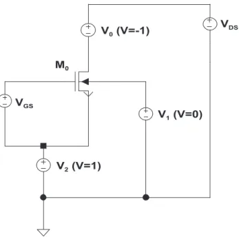
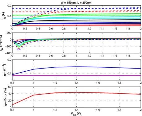
2.8 Test-bench used to get the I − V characteristic of a single NMOS device. . . 39
2.9 Comparison between I −V characteristics achieved from Spec-tre and from simplified equations. . . 41
2.10 Two dimensional projection of mixer O. . . 43
2.11 Comparison among different measures of mixer second order intermodulation distortion (IM 2). VRF is the input signal power while Second Order Power is mixer output at 1 MHz. . 44
2.12 Comparison between IM 3 provided by Simulink and Spectre. VRF is input signal power (two tones with same amplitude), while Third Order Power is mixer output at base-band. . . 48
2.13 Block diagram of the Time Discrete Model of the mixer. . . . 49
3.1 Schematic of the nMOS inductively degenerated LNA. . . 56
3.2 Schematic of the npMOS inductively degenerated LNA. . . 57
3.3 Comparison of intermodulation distortion amplitude at the mixer input port. . . 59
3.4 Behavioral model of the receiver. . . 60
3.5 Schematic of mixer test-bench if the mixer was characterized with an input voltage source. . . 66
3.6 Schematic of mixer test-bench used for characterization. The mixer is driven with a current source. . . 67
3.7 Projections of LNA and mixer P. For the mixer a plot of IRN (Input Referred Noise) versus Power is reported, for the LNA NF (Noise Figure) versus Power. . . 69
3.8 Evolution of FP. . . 70
3.9 Two dimensional projection of the receiver O. . . 72
3.10 Examples of convex and non-convex sets. . . 76
3.11 Example of convex function. . . 77
3.12 Diagram of E(X) versus X when n = 1. To reach the global minimum an uphill move is needed. . . 78
LIST OF FIGURES v 3.13 LNA configurations generated during optimization projected
onto the NF-Power space. Blue circles correspond to npMOS instances, red crosses to nMOS instances. The black circle is the optimal LNA configuration. It can be inferred that after an initial exploration phase alternating both topologies, simulated annealing finally focuses on the nMOS topology to
converge. . . 81
4.1 One subset of a modern vehicles network architecture. . . 85
4.2 Past and projected progress in dynamic driving control systems. 86 4.3 Example of a conventional RC oscillator schematic. . . 88
4.4 Block diagram of the proposed RC oscillator. . . 90
4.5 Simplified block diagram. . . 91
4.6 Voltage ramp on the capacitor while charging. Delay and in-put offset of the comparator cause an error on the voltage value at the end of the ramp. . . 93
4.7 Simplified block diagram. . . 95
4.8 Schematic of the compensation block. . . 95
4.9 Final schematic of the integration block connected to the com-pensation one. . . 98
4.10 Waveforms related to Fig. 4.9. . . 99
4.11 Schematic of a topology that is usually exploited to generate two non-overlapping signals starting from a clock IN . . . 104
4.12 Schematic of the block V-TO-I. . . 106
4.13 Schematic of the block VOLTAGE DIVIDER. . . 107
List of Tables
2.1 UMTS tests used for receiver performances. . . 29 2.2 Mixer input parameters bounds. . . 34 2.3 Output Performance Space for LNA, mixer and receiver. . . . 35 2.4 Characterization process results. Ieff/I measures the
effec-tiveness of ACG constraints in reducing the number of simu-lations required for performance model generation. . . 42 2.5 Mixer performance evaluation setup. . . 46 2.6 Frequencies, amplitudes and phases of all signals that compose
the output of a 3rd order non-linear block as a response of a
two pure tones input. . . 52 3.1 LNA performance evaluation setup. . . 58 3.2 Comparison between receiver behavioral simulations and
Spec-tre simulations. Rows show (for different quantities) the per-centage of receivers providing an error lower than the value in column. . . 73 3.3 Optimization results as a function of different cost functions.
Columns report, respectively, optimizations performed with: 1
°, no constraints other than UMTS compliance; °, as in2 1
° but with rewards for NF<NFmin; °, with same gain as3
reference design; °, as in4 ° but with 2 dB of NF margin3 with respect of NFmin;°, as in5 ° but with area penalty and4
1.5 dB of NF margin. The last column reports the reference design performances. . . 74 3.4 Performance of optimal receiver configuration and nearest
neigh-bors (NN) for optimization°. NN are not far from optimiza-2 tion result, which shows that performance extrapolation in P was moderate. . . 79
LIST OF TABLES vii 3.5 Performance of LNA corresponding to optimal receiver
config-uration and Nearest Neighbors (NN). . . 80 3.6 Performance of mixer corresponding to optimal receiver
con-figuration and nearest neighbors (NN). IIP2 is saturated at 80dBm. . . 83 4.1 Main specs of the implemented circuit. . . 89 4.2 Main drawbacks of the topology reported in Fig. 4.3, and
solutions adopted during this work. . . 103 4.3 Main characteristics of the implemented circuit (Std stands
Introduction
Over the last few years, terms like System-On-Chip (SOC) and Time-To-Market have become of utmost importance in the field of integrated circuits. All the main functions that can be useful to produce the final product are placed on the same chip. The first aim of the analog part is acquiring the signals coming from the environment and converting them in digital ones. Then a digital system is adopted to process them. Since the complexity of the operations to be performed by a chip is continuously growing, the digital part is growing at the same rate. Many functions that was assigned to the analog part in the past, nowadays are entrusted to the digital one. However, as long as the environment is “analog”, analog designers will never lose their job. Analog design is like the surface of a balloon: the more you blow, the more the thickness of its surface shrinks; but if the surface breaks, the balloon can’t survive as well.
Telecommunications and automotive are two fields where the coexistence of analog and digital circuits is widely used. In the first case, for example, the reception and the transmission of the signals exploit analog circuits, while the digital part provide many services to make the system and the user interface work. In automotive applications, instead, many analog circuits are dedicated to the conditioning of the signals coming from the sensors that are on board, while the digital blocks carry on the elaboration of all data.
This scenario shows how the digital and the analog worlds must grow side by side to give the final product to the customer. Nevertheless, the digital design flow is well supported by tools that provide automatic steps, whereas its analog counterpart is not: the synthesis of a digital circuits is made in an automatic way via environments like BuildGates, while the part of back-end is driven by softwares such as NanoEncounter. In the analog case, instead, the sizing of a circuit and the layout need much more to be customized. They are thus left to the designer experience and can rely on very few automatic routines. Hence it is a matter of fact that analog design
ix is becoming a bottleneck in the development of new SOCs.
This Ph.D. thesis focuses on trying to reduce the aforementioned gap between the analog and the digital flows. In details, this work copes with the design of analog integrated circuits exploiting and developing also new frameworks and methodologies to help designers during their job. The main goal of this research is then providing some new tools to perform the char-acterization of an analog circuit in an automatic way and to make easier and faster the optimization of a complex system. A new design methodology based on the concept of Analog Platforms is proposed to reach these aims. As mentioned before, both the analog and the digital part are key issues in telecommunication and automotive applications. Therefore these fields are very suited (and challenging too) to be used as case studies for this work.
The work done during this three years of Ph.D. can be divided into three main activities: the study and development of a new analog design method-ology based on Analog Platforms; the optimization of a front-end for UMTS applications; the design of an RC oscillator for automotive applications with high accuracy of the oscillation frequency. Part of this work has been car-ried out in collaboration with the Electrical Engineering Department of the University of Pavia, Pavia, Italy, about the FIRB project “Tecnologie Abili-tanti per Terminali Wireless Riconfigurabili” in the field of the activity “Uso di piattaforme analogiche per l’esplorazione architetturale di un terminale multistandard”. Some activities have also involved Simone Gambini, who is now a Ph.D. Student of the University of California, Berkeley. Therefore the reader can find further information about these subjects on the companion thesis [1].
This thesis is organized as follows: after this Introduction, Chapter 1 introduces Analog Platforms, describing their features and abstraction prop-erties and focusing on how architectural constraints are propagated at the behavioral level. Chapter 2 focuses on the UMTS front-end architecture used as the case study for the bottom-up platform generation phase. Chapter 3 deals with the top-down design phase of the same front-end, introducing high level system constraints and deriving behavioral model accuracy require-ments based on sensitivity analysis. Design exploration is then performed through optimization. Chapter 4 shows the design and characterization of an RC oscillator for automotive applications with low sensitivity to temper-ature, supply voltage, process spreads and charge injection. Finally, Chapter 5 draws some conclusions.
Chapter 1
Analog Platform Based Design
This Chapter deals with the problems related to the system level analog design and how these problems can be faced exploiting a methodology based on the concept of Analog Platform. The meaning of Analog Platform is explained and all related topics are described.
1.1
The Concept of Analog Platform
Over the past decade, a number of efforts has been carried out to automate the design process [2], [3]. We can classify the efforts in two broad classes: front-end tools, where circuit optimization is performed at the schematic level, and back-end tools, where optimization is performed in terms of layout generation/place&route. Some attempts have also been done to merge the two problems into specialized cell generators ([4], [5]), but they only provide automatic synthesis for specialized blocks. Focusing on front-end tools, most of them operate on fixed topology/architecture and attempt to address the sizing problem with respect of a given set of objective performances. Among the academic tools that use simulation as the optimization engine we can point DelightSpice [6], Anaconda [7], Astrx/Oblx [8] to mention but a few. Some commercial tools have also made their appearance in the last few years [9], all coupling sophisticated optimization algorithms (or mixtures of algo-rithms) and fully-accurate simulations. In [10], a method for examining the design boundaries is presented based on multiobjective optimization, evo-lutionary algorithms and multivariate regression schemes. Recently, several results have been obtained exploiting geometric programming to cast and solve the design problem. A number of academic works have been carried
1.1 The Concept of Analog Platform 2 System Specs System Design Circuit design Layout design n
n Based on previous designBased on previous design incremental improvement incremental improvement
n
n Experienced AnalogExperienced Analog Architects
Architects
n
n Shoot at feasibility ratherShoot at feasibility rather than optimality
than optimality
n
n Performance estimation atPerformance estimation at the heart of Top
the heart of Top-Down-Down flows
flows
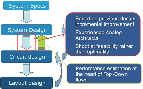
Figure 1.1: Traditional analog design flow.
out, dealing with operational amplifiers [5], LNAs, oscillators and so on. In-dustrial efforts are being carried out as well, with promising IP generator tools. However, none of the existing tools allows performing efficient sys-tem level design. Usually, individual components are designed/synthesized starting from a predetermined set of specifications. System level design tools should address the challenge of raising the level of abstraction so that not only an optimal set of specifications can be determined for individual block design, but all the tradeoffs can be evaluated at the system level, possibly including the analog/digital boundary. The development and application of top-down methodologies to analog design has been proposed more than ten years ago [11]. A number of case studies have been produced to demonstrate the advantages and the effectiveness of the approach [12], but the lack of general supporting tools has made its application quite cumbersome in real cases.
Platform based design has been recently proposed as an effective design methodology for dealing with the increased complexity of modern designs, facilitating design exploration, IP reuse and integration of complex systems [13]. Platforms have gained wide acceptance in the digital arena, and a num-ber of tools and methodologies are making their appearance based on this paradigm [14]. The platform concept has been formalized in the analog envi-ronment as well [15], however the lack of proper supporting tools has made its
1.1 The Concept of Analog Platform 3 S y st e m L e v e l S y st em L e v e l E x p lo ra ti o n E x p lo ra ti o n C ir cu it C ir cu it S iz in g a n d S iz in g a n d S y n th e si s S y n th e si s
l System SpecsSystem Specs
l Behavioral Models:Behavioral Models:
--MatlabMatlab,,Simulink, …Simulink, …
--Define Block RequirementsDefine Block Requirements
l Circuit Design:Circuit Design:
--Sizing, Simulation and IterationSizing, Simulation and Iteration
l Layout Design:Layout Design:
--Verification and IterationVerification and Iteration
Analog Platform
Analog Platform
Analog Platform
Analog Platform
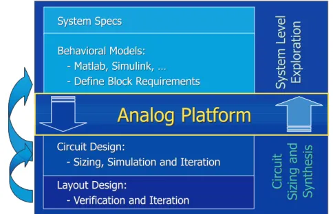
Figure 1.2: Analog design flow with the introduction of the Analog Platform.
application to meaningful designs rather difficult. Analog design has shown considerable resilience to attack in the direction of developing top-down flows and high level design practices. Even though high level mixed-mode lan-guages are becoming increasingly used, they cannot solve the performance estimation issue that plagues analog methodologies. High level behavioral models have been proposed for several classes of circuits and with different accuracy/complexity tradeoffs. Traditionally, behavioral models are used in two complementary ways:
1. During the early design stages and starting from the system specs given by the customer, simple models are introduced to test the overall sys-tem functionality and estimate sensitivities with respect to some per-formance figures (usually measuring non-ideal effects). By this way, the system architect tries to carry out one system structure (even if it is not the best one) that is suitable to fit the project specs. Then, actual design proceeds partitioning specification on the analog subsys-tem based on past design experience and with some hints provided by functional high-level simulations (see Fig. 1.1). Hence the circuit design is mainly based on previous designs incremental improvements and designer’s experience. Besides, this process is shoot to feasibility rather than optimality: circuit designers are usually satisfied once the
1.1 The Concept of Analog Platform 4 system specs are reached, then their work can go on with the layout phase. This is also due to the fact that customers can’t wait much time to have the final product, so they are not interested in design optimization but in obtaining a working device according to specs. 2. In the bottom-up phase, behavioral models are used to verify the overall
system functionality, providing better accuracy than in the top-down phase since models can be derived with more expensive and accurate extraction techniques, such as model order reduction [16], [17].
However, the expensive extraction process makes their exploitation in top-down phases unpractical since a large number of circuit sizings is required for effective design space exploration. Analog Platforms (APs) have been introduced to provide a new abstraction level for system level analog design-ers and facilitate design space exploration, so that an effective decoupling is achieved between system level analog design and circuit design and synthesis (see Fig. 1.2). APs couple the top-down functional use of behavioral models with the bottom-up performance estimation use to allow optimal design at the system level.
An Analog Platform is a pre-characterized library of components that can be used to implement analog functionalities [15]. It consists of behavioral models µ(in, out, ζ), interconnection models ι(in, out, ζ) and performance models P(ζ). µ(in, out, ζ) is parameterized executable model, which intro-duces at the functional level a number of non-idealities due to the actual circuit implementation. ζ is a vector of parameters controlling non ideali-ties and second order effects of behavioral models, such as gain, bandwidth, noise, etc. Behavioral models usually introduce a number of non-idealities in system simulation but as functional model unbound from any architectural effect. Finally, ι(in, out, ζ) is a parameterized executable model, which is used to describe the interface between two blocks A and B.
Differently from common approaches based on simulations that rely on regression schemes (such as [18]), in this work relations to model performance parameters by means of characteristic functions are used. Given a behavioral model µ(in, out, ζ), a performance model P constrains µ to feasible values of ζ (P(ζ) = 1). Performance models are defined by:
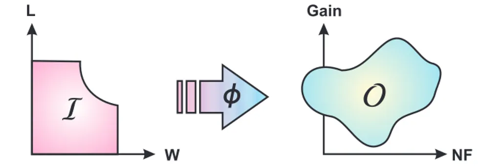
1. Input space I - Given a circuit C and m parameters κ controlling its configuration, IC ⊆ Rm is the set of κ over which C will be
1.1 The Concept of Analog Platform 5
I
L WO
Gain NFf
Figure 1.3: Illustration of Input Space, Output Space and Evaluation Func-tion.
2. Output space O - Given a circuit C and n performance figures ζ charac-terizing its behavioral model, OC ⊆ Rnis the set of ζ that are achievable
by C.
3. Evaluation function φ - Given a circuit C, IC and OC, φC : I → O
allows translating a parameter m-tuple set into a performance n-tuple set (see Fig. 1.3).
4. Performance relation P - Given a circuit C, IC, OC and φC, the
perfor-mance relation of C is defined to be PC on Rnthat holds only for points
o ∈ OC.
Analog Platforms also address composability of behavioral models to al-low hierarchical design fal-lows. APs provide a set of interconnection mod-els ι(in, out, ζ) to allow accurate model composition. In fact, analog circuit composition may significantly alter single circuit behavior, while behavioral model composition is a pure mathematical operation with no intrinsic side effects and loading notion. Unfortunately, no general guidelines are available for interface model generation. A correct-by-construction (even though po-tentially inefficient) modeling guideline consists of identifying a set of factors λ = [λSλL] that characterize the interface (both the source and load sides)
and of using them to derive composability rules. In the linear case, λ may be the vector of source and load impedances. λ is then appended to the performance vector ζ, so that the loading effect of B on A in A → B can be accounted for. In fact, performances for A are simulated considering an equivalent load BL
eq (λAL), while performances for B are simulated with an
equivalent source AS
1.1 The Concept of Analog Platform 6 λ
A
B
AeqB
λS eq BA
λLb) Characterization setup for platform A and B
a) Platform composition A driving B with interface paramater λ
Figure 1.4: Interface parameter λ during composition A-B and characteriza-tion of A and B.
(Fig. 1.4). Since λ is part of the performance vectors ζA and ζB, the
compo-sition rule imposes that performances for A and B are compatible with the interface loading and can be used to constrain behavioral models. On a case by case scale, however, more specific rules may be adopted for improving characterization efficiency and allow more flexible composition rules.
APs can be generated at multiple levels of abstraction and hierarchically organized into platform stacks. Platform stacks provide a unifying framework to model both the system abstraction hierarchy and the system refinement process. A key issue with platform stacks is that performance models con-strain behavioral optimizations/explorations to the feasibility region of the current platform level, so that the next level constraints are feasible and optimization can proceed to the next level. In abstract terms, platform stacks allow system tradeoff to be evaluated at high level of abstraction and propagate design choices to less abstract, more detailed design steps while maintaining feasibility requirement.
Design flow based on APs consists on two phases, bottom-up platform generation and top-down design exploration. Fig. 1.5 shows the bottom-up phase (the meaning of some concepts will be explained later on). Platform generation consists of selecting one or more circuit topologies and
characteriz-1.1 The Concept of Analog Platform 7
Figure 1.5: Bottom-Up Analog Platform generation.
ing circuit configurations (e.g. transistor sizings and/or bias) with parameter vectors κ (lying in a configuration space I) and circuit performances with vectors ζ (lying in a performance space O). Simulations are used to map κ into ζ, so that accuracy is achieved and no complex performance equations have to be derived. A performance model is then a relation P on ζ such that P(ζ) = 1 iff ζ is achievable with some vector κ and the current circuit topology and technology.
The top-down phase (see Fig. 1.6) consists of evaluating system per-formances at behavioral level and of performing optimizations to accurately explore the design space. Optimizations are intrinsically constrained by per-formance models to contemplate only feasible solutions for each block in the system, so that, independently of system level constraints and cost functions, optimization results are effectively achievable with some circuit configuration. The abstraction process involved in platforms allows optimizations to be run over several possible circuit topologies for each system component at once, thus effectively performing topology (architecture) selection as part of the optimization process.
1.2 Analog Constraint Graph 8
Figure 1.6: Top-Down system exploration.
1.2
Analog Constraint Graph
In [19] an approximation scheme for P based on Support Vector Machine (SVM) classifiers is presented based on statistical sampling of configuration vectors κ. However, the number of samples required to achieve good accu-racy levels increases exponentially with the dimensionality of κ. Besides, the mapping function φ(·) is usually a circuit simulator, which is much more ac-curate than manually derived equations, but of course orders of magnitude slower to execute. The characterization cost is thus exponentially depen-dent on the number of dimensions of the configuration space I, so that the characterization task might become unfeasible for moderately complex cir-cuits. However, even if I ⊆ Rn
, the n dimensions of I are usually strongly correlated if our attention is restricted to “working” circuits (let’s call them “good configurations”). A set of conservative constraints is enforced on κ [20], capturing simple circuit constraints necessary for correct circuit opera-tion. As an example, matching requirements, stacking of devices, operating region enforcement etc. introduce a set of constraints on κ that effectively reduces the size of I. Therefore, an effective Ieff can be defined as the subset
1.2 Analog Constraint Graph 9
ACG Configurations Good
Configurations
Figure 1.7: Representation of the Analog Constraint Graph behavior.
of I for which the following constraints hold:
fi(κ) + ǫi = 0 for i = 1 . . . n (1.1)
gj(κ) + ǫj < 0 for j = 1 . . . m (1.2)
where ǫi, ǫj are quantities that for approximate equations introduce slack
conditions as to enforce conservativeness. A set of constraints is conserva-tive when Rn
\ Ieff corresponds only to incorrect (as far as constraints are
concerned) circuits, even though some incorrect circuit may be generated for some κ ∈ Ieff. A non-conservative set of constraints can bias the performance
model excluding configurations that may actually be useful during the sub-sequent exploration phase. Since constraint equations are usually analytic approximations of the underlying circuit relations, conservativeness of con-straints must be explicitly enforced through ǫi, ǫj and/or accurate relations.
The exploitation of configuration constraints is very important to properly bias circuit sampling so that approximations of P be obtained efficiently. In non-degenerate cases, the n + m constraints in (1.1) and (1.2) provide an under-constrained system of equations for the value of κ, but determine a configuration space Ieff whose size is much smaller than the hypercube
Q[κmin
i , κmaxi ].
Platform designers can provide a set of constraints using simple analyt-ical models as a by-product of circuit design. The efficiency of the charac-terization increases with the larger number of constraints available, unless conservativeness is violated. The most useful way to represent (1.1) and (1.2) is through a bipartite undirected graph, which will be referred to as
1.3 Performance Model Approximation 10 Analog Constraint Graph (ACG). Fig. 1.7 illustrates the conservativeness concept in a graphical way. The “ideal” ACG should generate only good working circuits, rejecting all bad ones. Since this is not possible (and nei-ther safe!), a “well done” ACG must include at least all good configurations, while some bad ones could also be generated. Therefore the figure represents a bad situation, where the ACG rejects also a region in which good sizings are present (i.e. the pink ellipse should be entirely included in the light-blue one). ACGs drastically reduce the effective number of simulations required to get performance models, so that a few thousand simulations are sufficient for platform generation. Bipartite graphs are a natural way to operate on systems of equations, as implemented in the DONALD workbench [21] in the analog arena. Statistical sampling can leverage the graphical represen-tation of constraints to obtain an executable way of drawing samples in Rn
such that (1.1) and (1.2) hold and enforce conservativeness using properly distributed random variables for ǫ. This can be translated into a scheduling operation on the ACG which results in an efficient configuration generator. A node ξ in an ACG is said marked if a value or a random variable (and consequently a probability density function (pdf)) is assigned to it. Given an analog constraint graph and a set of marked nodes, the problem of gener-ating κ vectors can be seen as a graph scheduling problem that provides an execution order for marking all variables. Usually, initial markings consist of pdfs so that the overall graph can be seen as a graphical model for the pdf of κ. By choosing different random variables (Gaussian, exponential, etc.) or marking different node sets as initial marking, the overall pdf of κ can be altered thus biasing sampling in different ways. Eventually, mixtures can be used to achieve more thorough sampling (see also Section 2.3.2).
1.3
Performance Model Approximation
The problem of finding a representation for P can be casted as an approxi-mation problem. In this work, a Support Vector Machine (SVM) is adopted as a classifier as described in [19]. SVMs provide a favorable approximation scheme since they lead to compact models with smooth approximation and good generalization properties. In particular, SVMs with a Gaussian RBF kernel are used, which provide a basis function for the approximation of the form: f (x) = sign( SV X i αie−γ|x−xi| 2 − ρ) (1.3)
1.3 Performance Model Approximation 11 where vectors xi are performance vectors obtained through simulations and γ
is a kernel parameter that controls approximation features. The coefficients αi, ρ are weight and bias parameters that can be efficiently computed solving
a convex problem. xi are a subset of the simulated ζ also selected through the
convex problem. Since only SV vectors useful for classification are retained (Support Vectors), compact performance models can be obtained. γ sets the “width” of the exponentials in the summation (1.3), thus controlling the influence of (simulation) vector xi in classification of candidates ζ in some
ball around xi. As with any classifier, the goodness of an approximation f (x)
can be measured by two quantities, the rate of false negatives F N (feasible ζ that are discarded) and the rate of false positives F P (unfeasible ζ that are accepted). By construction, the approximation is built based only on feasible samples, so no explicit penalty can be exploited for false positives. The only means of controlling F P is through the kernel parameter γ at the cost of penalizing the generalization capabilities of the approximation (classifier).
Large values for γ minimize F P but easily discard feasible (unobserved) points (increasing F N ). Since γ is not automatically selected by the used SVM formulation, some quantitative and meaningful parameter must be pro-vided that allows γ to be determined. Even more importantly, the approxi-mation accuracy depends on the number N of performance vectors (number of simulations to run). Good values for N are strongly dependent on the particular platform being modeled, therefore a criterion for selecting optimal values for N is required. Implementing a set of heuristics, optimal values for γ and N are automatically selected. The heuristics are based on tradeoffs be-tween F N and F P . The number of F N can be easily measured evaluating P with a portion of simulation data not used for approximating P or by means of some n-fold cross-validation technique. Since there is no constructive way to test for false positives, random data are used to estimate F P according to the following observations:
1. false positives are independent of the used approximation, therefore F P is independent of γ;
2. the number of positives (performance vectors classified as feasible) that are get evaluating P with random data can be decomposed into a (con-stant with γ) number of real F P and a number (variable with γ) of apparent F P ;
3. F P increases as N increases.
1.3 Performance Model Approximation 12 1. the number of false negatives increases linearly with γ: F N = µ · γ; 2. the number of positives decreases exponentially with γ: P = F P∞+
e−(λ1+λ2·γ);
3. the rate of increase of F P (estimated with F P∞) decreases with N and tends to 0 for N → ∞.
The number of positives P obtained with random samples can be interpreted as a measure of the size of the model P:
P = Z RnP(ζ)dζ ≈ PRS 1 P(ζi) RS (1.4)
where the integral has been computed with a Montecarlo approximation on the RS random samples. For increasing N , new features (performance vec-tors) are added to the model, so P increases. However, as the approximation of P becomes good, it is more and more unlikely that new performance vec-tors ζ introduce new features, so ∂P
∂N decreases (P is a non decreasing function
of N ). Based on these observations, the following heuristics are adopted to determine the optimal value of N :
∂P ∂N
P 1
N < η (1.5)
which is the rate of variation of P with a penalty term N−1 that is used to
improve convergence. Both P and ∂P
∂N are measured at run time denoising
estimates of (1.4) with a weighted LMS polynomial fitting. The parameter η controls the accuracy of the approximation with respect of generalization capabilities (i.e. absolute F N rate).
The optimal γ can then be selected trading off the rate of increase of F N (generalizing approximation relative to a fixed N ) with the rate of decrease of F P (conservative approximation) according to:
µ ncv
= σλ2· e−(λ
1+λ2·γ)
F P∞ (1.6)
where σ controls the tradeoff between F P and F N and ncv is the number of
cross validation samples used to estimate µ. Condition (1.6) is independent of the cross-validation data set size and on the pdf used to generate random samples to estimate F P (as well as on their number).
1.4 Characterization Tool 13
1.4
Characterization Tool
By a practical point of view, generating the performance model P has two main aims: the first one is exploring the design space of a certain topology, the second one is exploiting that model in a high level analysis of a more complex system. As it will be shown in Chapter 2, the steps below must be followed to generate the performance model of a chosen circuit (and thus a chosen topology):
1. Choosing the Input Space I: the design space of the circuit has to be explored, so the schematic must be sized in many different ways (e.g. 2000-3000) to get the corresponding performances. Therefore the sizes to be varied must be chosen: some/all circuit device sizes, such as width and length of MOS transistors, biasing currents, resistors, etc. Once I has been chosen, the sizes usually reported in a schematic as numbers must be substituted with parameters (e.g. W, L, I, R, etc.). 2. Choosing the behavioral model µ: this step is necessary only if the AP
will be used for a system level design. This is not the case, for example, if designers are interested only in exploring the design space of the single circuit. Since the model must act in a different way according to the sizing of the corresponding schematic, µ must be parameterized (ζ). 3. Choosing the Output Space O: the performances of interest must be
chosen, such as power dissipation, gain, noise, etc. If a behavioral model is needed (see above), output parameters must include at least all parameters that appear in ζ, because they must characterize µ. Otherwise designers can choose performances as they like.
4. Providing an ACG to determine Ieff: the ACG must be implemented
somehow to generate the configurations that will be simulated.
5. Characterizing the AP: simulations must be performed and output per-formances must be get in an automatic way.
6. Performing the performance model approximation described in Section 1.3: while data come from the simulator, they must be post-processed to generate P. When the SVM learning process “has learnt enough”, simulations must be stopped.
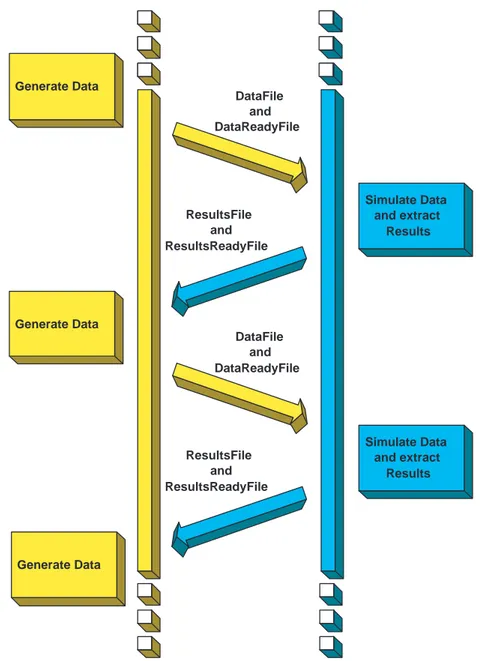
A supporting tool has been developed to drive the aforementioned process. The adopted solution relies on a client/server paradigm (see Fig. 1.8):
1.4 Characterization Tool 14 DataFile and DataReadyFile ResultsFile and ResultsReadyFile Simulate Data and extract Results Simulate Data and extract Results Generate Data Generate Data Generate Data DataFile and DataReadyFile ResultsFile and ResultsReadyFile
Figure 1.8: Message sequence chart for the Matlab/Ocean client/server syn-chronization.
1.4 Characterization Tool 15 • The client side is implemented in Matlab, relying on specific classes for performance models and ACG, and on C++ libraries for generating and manipulating SVM-based approximations. The ACG (and its sched-uler) is thus implemented with a Matlab script, where all parameters of I are set through a number of equations and disequations.
• The server side is based on the Ocean scripting language from Cadence [22] to implement a program that simulates circuit configurations, ex-tracts and post-processes output performance figures and finally sends the results back to the client.
Synchronization is achieved through semaphores, while the SSH protocol has to be used (through Cygwin on Windows) to transfer files since Mat-lab runs on Windows machines whereas Cadence runs on Unix Workstations (at present, both Cadence and Matlab can work efficiently on Linux, so the characterization process could be done in a different way). The invocation of Ocean is also done by Matlab, so the user needs only one Windows machine. The main script, which controls the whole characterization process, is in Mat-lab. First of all it calls the ACG script, which generates some configurations κ, let’s suppose 100. Then it sends these configurations written in a text file (DataFile1) to Ocean, together with another text file (DataReadyFile1) used as semaphore. When the Ocean script (server) receives DataReadyFile1, it reads DataFile1, sizes the schematic according to the first configuration κ1,
simulates it, gets output performances ζ1, writes them in a text file
(Re-sultsFile1), reads again DataFile1, simulates the second configuration κ2 and
so on. Once Ocean has simulated 100 κs (i.e. all received data), it sends back ResultsFile1 to Matlab. Besides, it sends also a text file named Result-sReadyFile1 to the client for synchronization. The number of results might not coincide with 100 because of two main reasons:
1. The AP designer could have chosen to prune some results if for instance some performances are out of defined bounds (e.g. power consumption is too high or gain is too low or noise is too high, etc.). This is a good idea because the ACG generates configurations using very simple equations, so it is not guaranteed that they really will give good output results after simulation.
2. Some simulations have been skipped because of environment (Cadence) errors, so they have not provided any results.
1.4 Characterization Tool 16 Due to the aforementioned considerations, when the ResultsReadyFile1 ar-rives to Matlab, Matlab counts the number of results in ResultsFile1. If they are above a threshold decided by the user, the SVM executes its post-process on them. Otherwise, Matlab generates new data through the ACG and sends them back to Ocean to obtain further results. This mechanism goes on un-til the threshold is reached, thus creating some sub-cycles inside the main process. This is done to be sure that the SVM makes its approximation on a quite high number of ζs. Let’s suppose that the acceptable threshold is 80% of the received results (the threshold applies to the actual main cycle of the characterization process). Then the desired results are 80 since the generated κs were 100. Now suppose that the returned results are 50. Since 50 is half of 100, then Matlab makes the assumption that the server has a rendering equal to 50%. Therefore, to reach the goal of 80 ζs, Matlab doesn’t generate 80 − 50 = 30 new κs, but (80 − 50) · 2 = 60. In general terms, if α is the percentual threshold, Mn is the number of results sent back by Ocean
in the n-th sub-cycle, and N is the number of the κ vectors generated in the actual main cycle, this mechanism applies the following adaptive equation until j X n=0 Mn≥ α · N: Zj = (α · N − j−1 X n=0 Mn) · Zj−1 Mj−1 (1.7) where Z is the number of configurations to be re-generated (thus Z0 = N ) and
j = 1, 2, 3 . . . is the number of sub-cycle. Referring to the previous example: α = 80%, Z0 = N = 100, M0 = 50, thus Z1 = (10080 · 100 − 50) ·10050 = 60.
As said before, after the tool exits from the sub-cycles explained above, the SVM approximation of all received ζ vectors takes place. If the approxi-mation of P is accurate enough (in the sense explained in Section 1.3), Matlab stops the characterization process. Otherwise, the main cycle goes on start-ing the second iteration (100 new configurations sent to Ocean, simulated, etc.).
The generation of P usually ends when the number of simulation runs is about 2000 or 3000 (an example of the learning process is reported in Fig. 3.8). Given this quite high number of iterations, a big effort was dedicated in achieving robustness with respect of possible simulation crashes, eventually providing also recovery mechanisms to resume the characterization process without restarting from the beginning. These mechanisms are really used
1.4 Characterization Tool 17
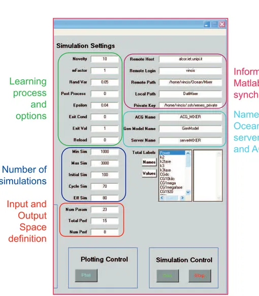
Figure 1.9: Graphic User Interface (GUI) main window.
only if the characterization is stopped by the user, because the tool has proved to be very robust.
In order to customize the characterization of different platforms, the user has to setup performance model parameters, provide an ACG scheduler (on the client side) and customize an Ocean server template with specific simu-lation setups and performance extraction code (on the server side). With a little of familiarity with the simulator, however, it is possible to obtain most of the code directly from the Analog Environment of Cadence, leaving to the user a simple cut&paste task to finalize the server.
To assist the user through the characterization process, an interactive Graphic User Interface (GUI) has been created exploiting Matlab abilities on the client side. Fig. 1.9 shows a picture of the GUI main window. The GUI allows the user to insert all the parameters necessary to Input and Output space definition (to control configurations generation and characterization process) and to explore simulation results. The form is divided into two main parts: Simulation Settings and Plotting Window.
Fig. 1.10 shows the part of the GUI that is dedicated to control the characterization process. The user can/must fill the following fields (some
1.4 Characterization Tool 18 Learning process and options Number of simulations Input and Output Space definition Information for Matlab-Ocean synchronization Names of Ocean server and ACG
1.4 Characterization Tool 19 fields are mandatory because they change from AP to AP; some others can be modified according to user’s needs or left as they are set by default):
1. Learning process and options: parameters for the SVM approximation and options (for example to reload the characterization if previously stopped before ending).
2. Number of simulations to run: minimum and maximum number of simulations, number of data to send to Ocean at first cycle and at each following one, threshold explained above.
3. Input and Output Space definition: size of I and O.
4. Information for Matlab-Ocean synchronization: the address of the re-mote host (Unix Workstation), the user name to access to Unix, the location of the password to access (the access is made through Private-Public key method) and the location of the Windows and Unix work folders.
5. Names of Ocean server and Matlab client scripts.
After completing the aforementioned form, the user can start the character-ization process.
At the end of the characterization process, the user can exploit the Plot-ting Window part to examine results. It allows the user to browse perfor-mance models, visualize two dimensional projections of P and interactively investigate (by zooming, visualizing mouse selected point coordinates, and so on) what the relations among different performances are, therefore allowing tradeoffs research. Each plot has the following features: crosses represent out-put performances corresponding to simulated configurations; colorbar gives informations about which performance values are achievable and which are not, according to SVM approximation of P: negative values correspond to different levels of unfeasibility, positive ones to different levels of feasibil-ity (see also Section 2.3.4). Some GUI abilities to explore two dimensional projections of P consist of:
• Visualizing a point corresponding to a chosen output performance con-figuration: this is especially useful if the characterization process is realized starting from a pre-existing design (that is our case), the formances of which are already known. Choosing to visualize this per-formances array, the user will be immediately able to compare new designs with the “starting” design.
1.5 Conclusions 20 • Dedicated zoom function: Matlab zoom function doesn’t work correctly with this kind of graphic objects. The main problem is to obtain the proper resolution and axes setting after the zoom has been performed. This dedicated function solves this trouble and also allows the user to set the desired axes ticks number.
• Visualizing at the same time all output performance values correspond-ing to a selected point on figure: if the selected point belongs to O, then the GUI shows directly the corresponding values; otherwise the GUI evaluates the point belonging to O and nearest to the selected one (nearest feasible point, called Nearest Neighbor in Section 3.9), and then returns the corresponding values.
• Highlighting the selected point and the Nearest Neighbor. • New Running Mode.
With New Running Mode we called a function that allows the user to enlarge the space O by simply making use of the mouse: users can select a certain region on the plot, in which they would like to get more performance results; GUI memorizes all performance points inside that region, generates new ran-dom κ configurations around those points and finally send them to Ocean to run simulations automatically. At the end of this new characterization, the space O and the figure present on the Plotting Window are updated, thus allowing an immediate comparison between old and new O.
1.5
Conclusions
In this Chapter a new methodology and characterization framework for build-ing Analog Platforms have been presented. A theoretical framework for auto-matic performance approximation has been introduced, and a configuration space pruning method has been developed with ACGs.
Chapter 2
Generation of Mixer Analog
Platform
This Chapter shows how an Analog Platform can be generated via the tool described in Chapter 1. A mixer used in a receiver front-end for Universal Mobile Telecommunication System (UMTS) applications has been exploited as a case study.
2.1
The UMTS Receiver
2.1.1
The UMTS Standard
The lack of available spectrum for the civilian wireless communications man-dates a multiple access technique to optimally exploit the limited resources. The resource to be shared can be time (Time Division Multiple Access or TDMA), power (Code Division Multiple Access or CDMA), or frequency (Frequency Division Multiple Access or FDMA). Obviously, the actual sys-tems can deploy in the same time two or more of these resources. For example GSM uses a frequency division multiplexing (FDMA) for the allocation of the frequencies, together with a time multiplexing (TDMA) allowing the use of the same frequency range by eight users at the same time. In CDMA the time slots and the frequency bands are the same for all users. The identifi-cation of one user among the others in the same bandwidth is obtained with a unique code sequence used to encode the information bearing signal. The receiver, knowing the code sequence of the user, decodes the received signal after the reception and recovers the original data. This is possible because
2.1 The UMTS Receiver 22 the correlation of the user code with the one present at the mobile unit is ideally one, while the cross-correlation with the other received codes is ideally zero.
In order to meet the growing demands of subscribers for different kinds of services, such as conferencing, multimedia, data base access, Internet, etc., it is necessary to have higher data rates up to 2 Mb/s and more stringent Qual-ity of Service (QoS) requirements with respect to first (1G), second (2G), and second and a half (2.5G or 2G+) generations of cellular telephony. The idea is to provide the same type of services everywhere, with the only limitation being that the available data rate may depend on the location (environment) and the load of the system. Therefore the third generation (3G) of cellular systems was born to address these issues. In January 1998 the basic technol-ogy for the Universal Mobile Telecommunication System (UMTS) Terrestrial Radio Access (UTRA) system was selected by the European Telecommunica-tions Standards Institute (ETSI). This decision contained the following key elements:
• For the paired bands 1920-1980 MHz (uplink: mobile transmits, base station receives) and 2110-2170 MHz (downlink: base station transmits, mobile receives), Wideband Code Division Multiple Access (WCDMA) technology shall be used in Frequency-Division Duplex (FDD) opera-tion.
• For the unpaired bands of total 35 MHz, instead, Time Division CDMA (TD-CDMA) technology shall be used in Time Division Duplex (TDD) operation.
The presence of the uplink and downlink bands indicates that the UTRA is a FDD system: working on different frequencies, it gives the opportunity to transmit and receive at the same time. It must be noted that one of the peculiarities of WCDMA systems is the time continuous transmission and reception, which can cause problems in reception because of the high trans-mitter signal leakage. Each paired band is divided into 12 channels centered 5 MHz apart from each other. Since the useful signal bandwidth is 3.84 MHz, then the difference between this band and the 5 MHz channel spacing guarantees margins for interference reduction between different operators.
Overall, UMTS is a 3G full-duplex standard based on WCDMA that is posing interesting challenges to the design community, mainly due to contin-uous transmission and reception.
2.1 The UMTS Receiver 23 LNA L.O. Mixer
Tx
1.96 GHz 2.1 GHz 2.1 GHz 0−2 MHzFigure 2.1: Direct conversion UMTS receiver architecture. The shaded area indicates the blocks considered in the case study.
2.1.2
Receiver Topology
A state-of-the-art UMTS fully integrated receiver front-end for mobile has been used as a case study to developed APs, thus testing both the character-ization methodology and the tool. The original design was provided by the Electronic Engineering Department of the University of Pavia, Pavia, Italy [23], [24], [25]. The front-end was designed with a 0.18µm STMicroelectronics CMOS process. Fig. 2.1 reports a block diagram of the UMTS receiver. APs have been developed for two topologies of LNA and one topology of mixer. The transmission (TX) section is not implemented but it is reported since it is the main source of interference for UMTS devices. The Local Oscillator (LO), even though implemented in the original design, has not been modeled during this thesis. The receiver exploit a Direct Conversion (DC) architec-ture. This means that the input signal is mixed with an LO at the same frequency, and translated directly to baseband. Since the bandwidth of the signal in the downlink band is 3.84 MHz, the useful bandwidth at baseband is 1.92 MHz. The main disadvantages of a DC Receiver (DCR) are DC off-sets, flicker noise, LO leakage and even order harmonic distortions [26]. For WCDMA applications, however, the DC conversion is very attractive because DC offsets and low frequency noise have to be integrated over the large signal bandwidth (1.92 MHz), so their relative importance is reduced [27]. The en-tire mobile receiver is shown in Fig. 2.2 with different details. It includes the antenna duplexer (a filter which strongly attenuates the interference signals at half the wanted signal frequency), the balun (balanced-unbalanced
exter-2.1 The UMTS Receiver 24
2.1 The UMTS Receiver 25 nal circuit to convert the single ended signal at the output of the antenna to a differential one), the LNA, the I&Q mixer (since the WCDMA technology ex-ploits Quadrature Phase Shift Keying (QPSK) modulation in downlink, two mixers driven by signals in quadrature have to be used), a programmable VGA with 4th order Butterworth filter, a second VGA and finally a 6 bits
A/D converter. The LNA can be realized with a classical source inductance degenerated LC resonant differential pair. The load is a resonant internal LC tank, which does some filtering on the out-of-band blockers (strong and unwanted adjacent channel interference signals), relaxing mixer linearity re-quirements. Second order non-linearities are unimportant in the LNA case as they are filtered off by the AC coupling between LNA and mixers. An active mixer has been chosen in order to reduce the noise requirements of the baseband blocks. Moreover, high linearities are difficult to achieve with passive mixers. An output pole was fixed at a nominal frequency of 8 MHz to alleviate the linearity requirements of the first VGA.
2.1.3
Some Useful Definitions
Each circuit can be considered as a non-linear system. If the power of the input signal is low enough, devices behave in a nearly linear way and non-linear contributions can be neglected. Hence only the fundamental harmonic of the input signal appears on system output. On the contrary, if the power is increased, harmonics different from the fundamental overcome the noise floor and become noteworthy. In RF circuits the non-linear behavior has a very high importance because non linear systems give rise to signal components that were not present in the input. Therefore, a signal that is theoretically out of the useful band might become an interferer due to its manipulation by a non-linear device.
Let’s consider an input signal with the following form
x(t) = A1cos (ω1t + φ1) (2.1)
and suppose to model the non-linearity with a third order polynomial y(t) = k1x(t) + k2[x(t)]2+ k3[x(t)]3 + . . . + kM[x(t)]M (2.2)
Under the assumption that A1 < 1 (an hypothesis usually referred to as
weakly non-linear behavior), the output of the circuit at the frequency nω1
2.1 The UMTS Receiver 26 1, 2, 3, . . . , M (see Section 2.3.6). The output at nω1 is thus proportional to
the n-th power of A1.
Now suppose to have an input like the one below:
x(t) = A1cos (ω1t + φ1) + A2cos (ω2t + φ2) (2.3)
In this case, also the so called intermodulation distortion is generated: the second order non-linear behavior of the circuit gives rise to signals at fre-quencies |ω1± ω2|, which increase with A1 and A2; the third order non-linear
behavior gives rise to signals at frequencies |2ω1 ± ω2|, which increase with
A2
1 and A2, and also to signals at |ω1± 2ω2|, which increase with A1 and A22,
and so on. In fact this is exactly true only if the non-linearity is of order M ≤ 3, because orders higher than three produce components that cause an increase (expansion) or a decrease (compression) of the aforementioned amplitudes.
Being V out(±a,±b) the amplitude of the output of the non-linear system at frequency ±aω1± bω2, the following definitions hold:
• Second Order Intermodulation Distortion: IM 2, ¯ ¯ ¯ ¯ V out(1,±1) V out(1,0) ¯ ¯ ¯ ¯ A1=A2=A (2.4) • Third Order Intermodulation Distortion:
IM 3, ¯ ¯ ¯ ¯ V out(2,±1) V out(1,0) ¯ ¯ ¯ ¯ A1=A2=A (2.5) • Second Order Intermodulation Intercept Point , IIP 2 , amplitude
A = A1 = A2 s.t. IM 2 = 1
• Third Order Intermodulation Intercept Point , IIP 3 , amplitude A = A1 = A2 s.t. IM 3 = 1
If M = 3 it is simple to demonstrate that the following hold (see 2.3.6): ½ IM 2 = |k2 k1|A IM 3 = 34|k3 k1|A 2 (2.6) hence: ( IIP 2 = |k1 k2| IIP 3 =q43|k1 k3| (2.7)
2.1 The UMTS Receiver 27
2.1.4
UMTS Tests
The following tests have to be performed to evaluate the main performances of a mobile receiver for UMTS applications. These tests will be exploited in Chapter 3 to optimize the entire front-end in power.
The starting hypotheses are: 1. TX power Class III
2. Duplexer TX to RX isolation = 44 dB 3. Duplexer insertion loss = 1.8 dB
The input signals to be used for each test are reported below: 1. Out-of-band IIP 3:
the specification on the third order linearity of LNA and mixer is es-sentially due to the presence of the transmitted signal leakage and to an out-of-band blocker. The test must thus be done in the following conditions:
• TX leakage = -30 dBm; frequency offset = 135 MHz
• Out-of-band blocker = -40 dBm; frequency offset = 67.5 MHz The frequency offset is referred to the LO frequency at the lower bound of the RX band, that is fLO = 2.1 GHz. Combining the aforementioned
frequencies and LO, the IM 3 would fall at DC. Hence the tones must be rearranged to move the IM 3 to a useful baseband frequency, for example 1 MHz.
2. In-band IIP 3:
the linearity specification of LNA and mixer given by the intermodu-lation test is much more loose than the one given by the out-of-band test. Therefore this test is not an issue for the RF section of a UMTS receiver. Anyway, the situation is the following:
• TX leakage = -48 dBm; frequency offset = 10 MHz
• Out-of-band blocker = -48 dBm; frequency offset = 20 MHz The frequency offset is referred to any LO frequency inside the UMTS band. As said before, the IM 3 would fall again at DC. Hence the aforementioned tones must be a little rearranged.
2.1 The UMTS Receiver 28 3. IIP 2:
this specification is determined by the leakage of the transmitted signal. Therefore the test to be done is:
• TX leakage = -30 dBm; frequency offset = 135 MHz
The frequency offset is referred to the LO frequency at the lower bound of the RX band, because this is the most critical situation. The IM 2 arises from the WCDMA modulation. The test can be simulated by using a DSB-SC signal, that is two tones with same power (-33 dBm). The frequency offset between these two signals must be set to a proper value, such that the intermodulation is reported (by the LO) to base-band at a useful frequency (e.g. 1 MHz).
4. Gain:
to evaluate this performance, only one input signal is required: • Useful signal = -30 dBm; frequency offset = 1 MHz
The frequency offset is referred to the LO frequency at the lower bound of the RX band. The exact power of the signal is not an issue, on con-dition that the receiver works linearly. The frequency offset is not an issue as well: using 1 MHz is only to measure the output signal at 1 MHz, that is inside the useful baseband bandwidth. Nevertheless, dif-ferent choices could be done, provided that the output signal frequency is between 10 kHz and 1.92 MHz. The 10 kHz lower bound has been considered according to [24].
5. Noise:
the total output noise of the whole receiver must be evaluated over the band 10 kHz → 2.2 GHz (while the band of interest for mixer only is 10 kHz → 1.92 MHz).
Tab. 2.1 summarizes the UMTS tests described above, also reporting the frequencies chosen during this thesis. The IM 3 shown in table refers to the out-of-band IIP 3 test. With those choices, both linear gain and IM 2 and IM 3 must be measured at 1 MHz at mixer output. The reasons of such choices can be found in Section 2.3.4.
Present Chapter focuses on the details of the generation of mixer plat-form, also illustrating the use of ACG. The description of a platform stack
2.2 Current-Commutating Mixers 29
Performance Input Signals Local Oscillator
Gain f1 = 2.101 GHz, -30 dBm fLO = 2.100 GHz
IM 2 f1 = 1.965 GHz, -33 dBm fLO = 2.100 GHz
f2 = 1.964 GHz, -33 dBm
IM 3 f1 = 2.030 GHz, -40 dBm fLO = 2.100 GHz
f2 = 1.961 GHz, -30 dBm
Table 2.1: UMTS tests used for receiver performances.
generation is given in Chapter 3, showing how a higher-level receiver platform can be built based on LNA and mixer ones.
2.2
Current-Commutating Mixers
The mixer used during this thesis is a current-commutating mixer. It is worth spending a few words to give to the reader a short overview about this circuit just to understand how it works. This kind of topology derives from the Gilbert cell presented in [28]. Please do consider the single-ended balanced CMOS circuit reported in Fig. 2.3. The small input signal vin (which is at
RF) is transformed into a current signal via the transconductor M RF . Then the generated current iRF passes through the switching couple M1−M2which
is driven in a differential mode by the Local Oscillator output VLO. Finally,
the current reaches R1 and R2 to produce the output voltage vout. M1 and
M2 can be considered as ideal switches at a first order analysis, since VLO is
a very large signal. Therefore the LO drives both MOSTs alternatively in triode region, thus modulating the output current:
iout(t), i2(t) − i1(t) = vin(t) · gmRF ·
gm1(t) − gm2(t)
gm1(t) + gm2(t)
(2.8) where gmRF, gm1 and gm2 are respectively the transconductances of M RF ,
M1and M2. This relationship can be expressed in a different form to highlight
the modulating action of the LO:
iout(t) = vin(t) · gmRF · m(t) (2.9)
where
m(t) = gm1(t) − gm2(t) gm1(t) + gm2(t)
(2.10) To understand the mixing action, let us make the simplifying assumption
2.2 Current-Commutating Mixers 30
Figure 2.3: Single-balanced Gilbert cell.
for m(t) to be a square wave toggling between +1 and -1 with a 50% duty-cycle and with the same period as the LO signal. This means that both M1
and M2 are on for 50% of the time. Besides, when M1 is on, M2 is off and
vice-versa. Although the results that will be derived apply rigorously only to the case of a perfect square LO signal wave with 50% duty-cycle, they can be easily extended to the case of a large amplitude sine wave LO (which is the real case). Since m(t) is a periodic odd signal, it can be written as a Fourier series with only odd coefficients:
m(t) = +∞ X n=−∞ cne j2πnt T0 (2.11) where T0 = fL01 , and: ½ c2n+1 = (2n+1)π2 c2n= 0 (2.12)
2.3 Mixer Platform 31 Therefore, the Fourier transform of m(t) is:
M (f ) =
+∞
X
n=−∞
cn· δ(f − nfLO) (2.13)
Finally, supposing to have R1 = R2 = RL, the expression of Vout(f ) comes
out to be the following: Vout(f ) =
+∞
X
n=−∞
cn· gmRF · Vin(f − nfLO) · RL (2.14)
Defining the single sideband Conversion Gain (CG) of the mixer as the ratio of the low-frequency output signal amplitude over the RF input signal am-plitude, that is the gain between the low frequency signal at the output of the switching pair and the high frequency signal at the RF transconductor, the CG of the single-balanced Gilbert circuit is given by:
CG, |Vout(fLF)| |Vin(fLF + fLO)|
= c−1· gmRF · RL= gmRF · RL·
2
π (2.15)
where fLF is one frequency inside the useful signal baseband bandwidth, i.e.
less than 1.92 MHz in the UMTS case. As will be shown next, the mixer used for the UMTS receiver exploits a double balanced topology with differential input transconductor (see Fig. 2.4). As a consequence, the expression of the CG is a little bit different:
CG, |Vout(fLF)| |Vin(fLF + fLO)| = (gm5+ gm6) · RL· 2 π (2.16)
2.3
Mixer Platform
2.3.1
Mixer Input Space Definition
As explained in Section 2.1, the original mixer is an I&Q mixer for direct conversion [24]. It downconverts the input signal frequencies shifting them by about 2.1 GHz (Local Oscillator tone) downwards. For characterization aims, considering both branches is not an issue. Therefore, a schematic with only one branch is used as it is reported in Fig. 2.4. We defined the input space I to include biasing currents and MOS sizes, since they most have