JOUL, Volume 4
Supplemental Information
Mechanically Stacked, Two-Terminal
Graphene-Based Perovskite/Silicon Tandem
Solar Cell with Efficiency over 26%
Enrico Lamanna, Fabio Matteocci, Emanuele Calabrò, Luca Serenelli, Enrico Salza, Luca Martini, Francesca Menchini, Massimo Izzi, Antonio Agresti, Sara Pescetelli, Sebastiano Bellani, Antonio Esaú Del Río Castillo, Francesco Bonaccorso, Mario Tucci, and Aldo Di Carlo
Supplemental Information
Figure S1 (A) Photoluminescence and absorbance of the perovskite absorber deposited over cTiO2/mTiO2 electron transport layer. (B) Tauc Plot analysis for optical bandgap estimation of the perovskite absorber.
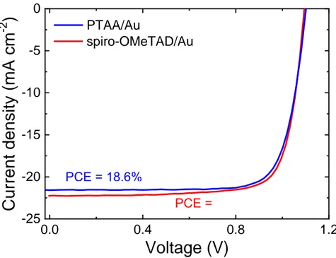
Figure S2 J-V characteristics of the reference mesoporous perovskite solar cells using spiro-OMeTAD (200
nm) or PTAA (40 nm) hole transporting layer and Au (80 nm) counter electrode. The J-V curves have been acquired in reverse voltage scan mode.
0.0
0.4
0.8
1.2
-25
-20
-15
-10
-5
0
Current dens
ity
(m
A cm
-2)
PTAA/Au
spiro-OMeTAD/Au
Voltage (V)
PCE = 18.6%
PCE =
19.0%
0.0 0.2 0.4 0.6 0.8 1.0 1.2 -20 -15 -10 -5 0
Voltage (V)
Cu
rren
t De
nsi
ty
(mA
cm
-2)
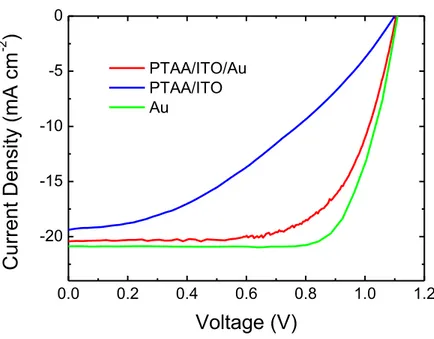
PTAA/ITO/Au PTAA/ITO AuFigure S3 J-V characteristics of the same small area graphene-based perovskite solar cell using PTAA/ITO
electrode before (blue curve) and after (red curve) Au deposition on ITO, compared against a cell from the same batch with the conventional Au electrode (green curve). The J-V curves have been acquired in reverse voltage scan mode.
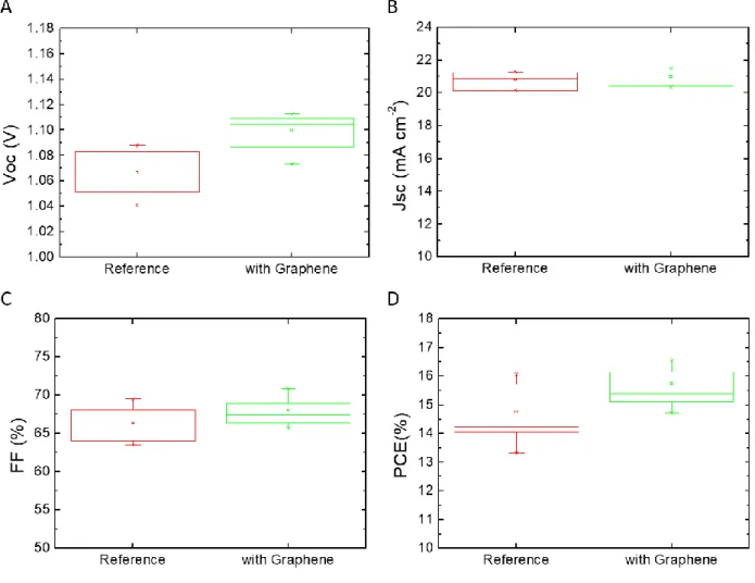
Figure S4 Statistical analysis of the Figures of Merit (FoM) of the small area perovskite solar cells with
PTAA/ITO/Au counter electrode with and without graphene doping: (A) open-circuit voltage (Voc); (B) short-circuit current density (Jsc); (C) Fill Factor (FF); and (D) power conversion efficiency (PCE).
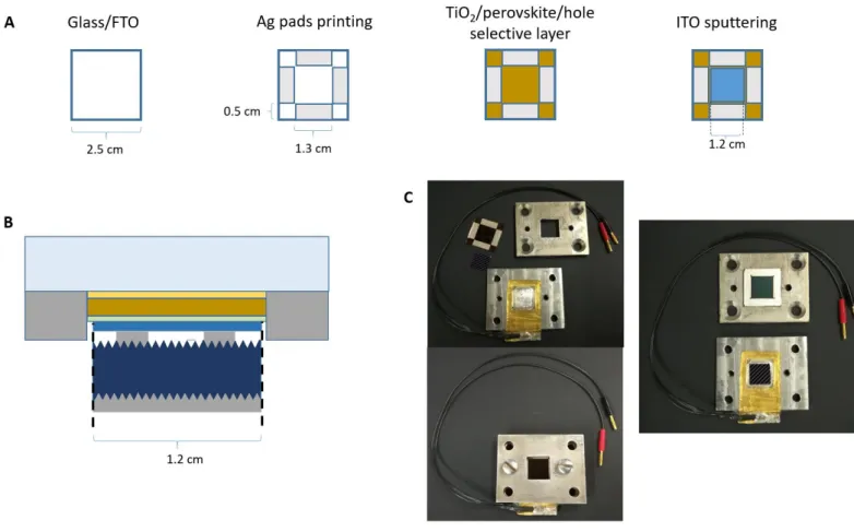
Figure S5 (A) sketch of the process flow of the perovskite solar cell, including the definition of the
substrate, contacts and active area dimensions; (B), image of the coupled cells showing the direct contact between the fingers of the silicon bottom-cell and the ITO back electrode of the perovskite top-cell; (C) Photograph of the measurement set-up used to keep the sub-cells in contact.
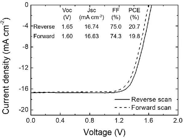
Figure S7Forward and reverse J-V scan of a perovskite/c-Si mechanically stacked tandem, without graphene addition. The hysteresis behavior is the same observed for other devices based on this tandem architecture
Figure S8 Statistical analysis of the PCE (estimated by J-V curves acquired in reverse voltage scan mode)
measured on 15 graphene-based perovskite/Si HJT tandem obtained by mechanically stacking different graphene-based mesoscopic perovskite top-cells over the same Si HJT bottom-cell.
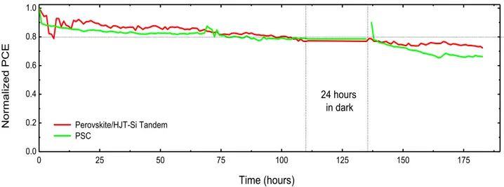
0 25 50 75 100 125 150 175 0.0 0.2 0.4 0.6 0.8 1.0 Perovskite/HJT-Si Tandem PSC No rmal ize d PCE Time (hours) 24 hours in dark
Figure S9 Stability of perovskite solar cell with ITO/Au electrode (green curve) and two-terminal
mechanically stacked perovskite/silicon tandem (red curve) under continuous simulated 1 Sun illumination.
Table S1 Statistical analysis of the FoM (estimated by J-V curves acquired in reverse voltage scan mode)
Device VOC (V) JSC (mA cm-2) FF (%) PCE (%) Perovkite/silicon HJT tandem 1.796 ± 0.008 17.955 ± 0.434 77.381 ± 0.856 24.970 ± 0.848