Jos 1:9.
Dedicado a mi amada esposa Diana, mi queridos padres Jorge y Martha, mis hermanas Catty y Valeria, mis hermanos, mis tesoros Paula y Victoria, mi familia y todas las personas que aportaron a mi vida durante todo este tiempo. Dios los colme de bendiciones!.
De todo corazón, quiero agradecer a Dios por haberme sostenido y provisto todos estos años. A mi dulce esposa, que no obstante todo, ha sabido darme su amor y apoyo en todas la circunstancias de este periodo. Un agradecimiento especial al Pueblo Ecuato-riano y SENESCYT, que hizo posible este sueño. Un sentido saludo y agradecimiento al Prof. Calogero Pace que supo como guiarme, fortaleciendo mis destrezas y retandome a alcanzar unas nuevas. Aprovecho para agradecer a STMicroelectronics en la persona del Ing. Giusseppe Consentino y mis amigos Donatella De Pasquale y Alessandro Dignoti. Un saludos por igual a todos los amigos(as) que conocí en el NexusLab, en especial a Carlo Giordano y Letizia Fragomeni que supieron brindarme su amistad y aporte inigual-able. Mi agradecimiento a la gran familia "Siloe" en la persona del Pt. Marco Lienhard y su familia que han aportado tanto a mi vida durante estos años. Finalmente, pero no menos importante, un reconocimiento a todas aquellas personas, amigos y ajenos, que estando en tierra lejana, me hicieron sentir como si fuera a casa!
Rende, novembre 2015 Jorge L. Hernandez Ambato
Nowadays electronic applications involve a high density of power Metal Oxide Semi-conductor Field Effect Transistors (MOSFETs) which represent the major percentage of energy flow to be controlled. Moreover, new technologies, such as Silicon Carbide (SiC), have been well involved in the existing power applications. Therefore, the reliability of power devices is highly demanded.
Since decades, a widely used accelerated test to evaluate the reliability of MOSFETs is the so-called High Temperature Reverse Bias (HTRB). In this stress test, the Devices Under Test (DUTs) are reverse polarized at a certain percentage of the rated breakdown voltage and maintained in this condition at high temperature for a determined long time. A typical HTRB test also incorporates Electrical Characterization Tests (ECTs) of DUTs before and after each stress period, seeking for failed devices. However, time elapsed between ECTs are long and degradation and failure information of DUTs might not be registered.
In this context, an advanced methodology for HTRB test is proposed. The latter consists of applying more stress cycles of short duration together with more frequent ECTs at a relatively high temperature that can be directly compared to that of normal operation in power applications (i. e. 125 °C). With this methodology, more detailed information about degradation trends in electrical parameters, time of failures and stop-ping of stress test on degrading devices before full breakdown can be performed. The latter can be very useful in R&D stages, where the post-failure analysis of well-degraded devices, but not broken, is important.
An automatized instrumentation, aimed to apply this methodology, has been im-plemented. The latter utilizes individual Thermal Control Modules (TCMs) to control the test temperature per single DUT. The temperature control is performed through an opposite mini-heater and firmware running on an 8-bit microcontroller. TCMs can be set remotely to apply test temperatures in the range [30-200 °C]. In addition, Switch Matrix Modules (SSMs) are implemented to configure the electrical connections required for HTRB or ECT tests remotely. A PC application controls all the modules through a Master Communication Module (MCM) also implemented. A commercial Source and Measure Unit (SMU) is used for the electrical stress. Full customization of HTRB and
at slightly different temperature are performed in the DUTs. In addition, accurate test results have shown that drawbacks of typical HTRB implementation have been solved through the advanced methodology and instrumentation reported.
Complementing the work presented, Low-Frequency Noise Measurements (LFNMs) were also applied as valuable tool to investigate the degradation process in power MOS-FETs after stressing them through HTRB test. A correlation between the results from advanced HTRB test and LFNM in power MOSFETs demonstrates that the electrical degradation is represented by a noise spectrum different to that for intrinsic 1/f noise.
Le applicazioni elettroniche odierne sono caratterizzate da un’elevata densità di tran-sistori ad effetto di campo di tipo metallo-ossido-semiconduttore (MOSFET) che rap-presentano dunque la maggiore sorgente di consumo di energia da gestire. Inoltre, nuove tecnologie, come quella basata sul Silicon Carbide (SiC), sono state impiegate nelle ap-plicazioni ad alta tensione/corrente. L’affidabilità dei dispositivi di potenza è dunque una caratteristica fondamentale.
Da decenni una tipologia di test accelerati largamente impiegata per valutare l’affi-dabilità dei MOSFET è quella denominata High Temperature Reverse Bias (HTRB). In questi test, i dispositivi da testare sono polarizzati inversamente ad una certa percentua-le della tensione di breakdown e mantenuti in queste condizioni ad epercentua-levata temperatura per un determinato intervallo di tempo. Tipicamente, prima e dopo ogni ciclo di stress, vengono effettuate delle caratterizzazioni elettriche (Electrical Characterization Tests -ECTs) al fine di valutare eventuali forme di degrado e fallimenti dei dispositivi. Tutta-via, gli ECT sono effettuati ad intervalli di tempo molto lunghi, quindi le informazioni legate ad eventuali forme di degrado e fallimento possono non essere rilevate.
In questo contesto, il lavoro di ricerca si è concentrato principalmente sulla defini-zione di una metodologia avanzata per la realizzadefini-zione dei test HTRB. La procedura proposta consiste nell’applicazione di più cicli di stress a breve durata, intervallati da caratterizzazioni elettriche eseguite a temperature relativamente alte, confrontabili con quelle che si raggiungono normalmente in applicazioni di potenza (cioè, 125°C). Impie-gando la metodologia proposta è possibile ottenere informazioni più dettagliate circa l’andamento del degrado dei parametri elettrici ed i tempi di fallimento dei dispositivi. Inoltre, la procedura prevede l’interruzione del test sui dispositivi degradati prima della completa rottura degli stessi. In particolare, quest’ultimo aspetto è rilevante nelle fasi di ricerca e sviluppo, dove l’analisi dei dispositivi danneggiati, ma non totalmente distrutti, consente di ottenere informazioni importanti.
Al fine di applicare la metodologia ideata, è stata sviluppata tutta la strumentazione richiesta. In particolare, questa impiega dei moduli di controllo che consentono di gestire la temperatura dei singoli dispositivi da testare (Thermal Control Module - TCM). Il controllo della temperatura è effettuato attraverso l’uso di adeguati mini-riscaldatori e
di tempo brevi, di gestire in real-time il controllo dei test HTRB. Queste caratteristiche sono utili per ottenere dati di affidabilità in un tempo più breve rispetto alle applicazione dei tipici test HTRB, permettendo inoltre di eseguire analisi successive ad i fenomeni di degrado.
La procedura descritta è stata applicata a dispositivi MOSFET realizzati in silicio ed in SiC ottenendo risultati interessanti e dimostrando, al contempo, che la metodologia ideata è adatta per l’esecuzione di test HTRB più brevi e più accelerati, in modo da acquisire informazioni necessarie per l’analisi dei processi di degrado e dell’affidabilità dei dispositivi di potenza. Inoltre, i risultati sperimentali hanno dimostrato che l’esecuzione più frequente di ECT a temperature leggermente diverse non impattano sugli andamenti di degrado dei dispositivi. Inoltre, la metodologia implementata consente di risolvere i principali svantaggi legati alle procedure standard di test HTRB.
In aggiunta a questo, il presente lavoro riporta l’applicazione di misure di rumore a bassa frequenza come utile strumento per investigare ed individuare i meccanismi di fallimento indotti dai test HTRB sui dispositivi MOSFET di potenza. Le misure effet-tuate dimostrano l’esistenza di una correlazione tra lo spettro di rumore dei dispositivi sottoposti a stress ed i relativi test HTRB: in particolare, i risultati ottenuti mostrano che lo spettro di rumore differisce da quello intrinseco rappresentato dal rumore 1/f.
Conference contributions
1. C. Pace, J. Hernandez-Ambato, and C. Giordano, "A Novel Instrumentation for an Advanced High Temperature Reverse Bias (HTRB) Testing on Power Tran-sistors," Applications in Electronics Pervading Industry, Environment and Society (APPLEPIES), 2014. (in edition)
2. G. Consentino, M. Laudani, G. Privitera, C. Pace, C. Giordano, J. Hernandez-Ambato, and M. Mazzeo, “Effects on power transistors of Terrestrial Cosmic Rays: Study, experimental results and analysis,” in Applied Power Electronics Conference and Exposition (APEC), 2014 Twenty-Ninth Annual IEEE, 2014, pp. 2582–2587, doi: 10.1109/ APEC.2014.6803667.
3. G. Consentino, D. De Pasquale, S. Galiano, A. D. Ignoti, C. Pace, J. Hernandez-Ambato, M. Mazzeo, and C. Giordano, “Innovative Instrumentation for HTRB Tests on Semiconductor Power Devices,” in AEIT Annual Conference, 2013, pp. 1–5, doi: 10.1109/ AEIT.2013.6666814.
4. G. Consentino, M. Laudani, G. Privitera, A. Parlato, N. Marchese, E. Tomarchio, C. Pace, C. Giordano, M. Mazzeo, and J. Hernandez-Ambato, “Dangerous effects induced on power MOSFETs by terrestrial neutrons: A theoretical study and an empirical approach based on accelerated experimental analysis,” in AEIT Annual Conference, 2013, 2013, pp. 1–6, doi: 10.1109/AEIT.2013.6666813. Journal papers
1. C. Pace, J. Hernandez-Ambato, D. De Pasquale, and G. Consentino, “Instru-mentation for Innovative Semiconductor Power Devices Reliability Tests,” Int. J. Eng. Ind., vol. 4, no. 2, pp. 119–127, 2013, doi: 10.4156/ijei.vol4.issue2.14.
ADC Analog to Digital Converter ADT Accelerated Degradation Testing AEC Automotive Electronics Council ALT Accelerated Life Test
CNP Charge Neutrality Point COTS Commercial On The Shelf DFT Discrete Fourier Transform
DMOSFET Double Diffused MOSFET DUT Device Under Test
ECT Electric Characterization Test
EECT Emergency Electric Characterization Test EVT Electric Verification Test
FIT Failures In Time
GPIB General Purpose Interface Bus GUI Graphical User Interface
HALT Highly Accelerated Life Testing HASS Highly Accelerated Stress Screening HTRB High Temperature Reverse Bias HTGB High Temperature Gate Bias
LTS Low Temperature Storage Life MCM Master Communication Module
MIL-DoD Military Department of Defense of United States MOSFET Metal Oxide Semiconductor Field Effect Transistor MS Mechanical Shock
MTTF Mean Time To Failure MTBF Mean Time Between Failure NI National Instruments
PC Power Cycling
PCB Printed Circuit Board PWM Pulse Width Modulation
PID Proportional Integrative Derivative PSD Power Spectral Density
RAT Reliability Acceptance Test R&D Research and Development RDT Reliability Demonstration Test RTS Random-Telegraph-Signal
SCPI Standard Commands for Programmable Instrumentation SEM Scanning Electron Microscopy
SMD Surface Mounting Device SMM Switch Matrix Module SMU Source and Measuring Unit TAT Thermal Adjustment Tool TC Temperature Cycling
TCM Temperature Control Module TST Thermal Shock Test
UART Universal Asynchronous Receiver-Transmitter USB Universal Serial Bus
VDMOS Vertical Diffused MOS
Abstract vii
Riassunto ix
Acronyms xiii
List of figures xxvi
List of tables xxviii
Introduction 1
1 Power Semiconductor Devices 3
1.1 Electronic Properties of Si and SiC . . . 5
1.1.1 Carrier Mobility Parameter . . . 5
1.1.2 Impact Ionization . . . 6
1.2 Structure of a Power MOSFET . . . 10
1.3 Electric Characteristics of Power MOSFET . . . 11
1.3.1 Breakdown Voltage Parameter . . . 12
1.3.2 Drain Leakage Current Parameter . . . 16
1.3.3 On-Resistance Parameter . . . 18
1.3.4 Gate Leakage Current . . . 22
1.3.5 Threshold Voltage Parameter . . . 23
1.4 Noise in Semiconductor Devices . . . 26
1.4.1 Power spectral density . . . 27
1.4.2 High Frequency Noise . . . 28
1.4.3 Low Frequency Noise. . . 30
2 Reliability Testing on Power Devices 39 2.1 Why Reliability on Power Semiconductor Devices? . . . 40
2.2 Reliability Concepts . . . 41 xvii
3 High Temperature Reverse Bias: Instrumentation Development 55
3.1 HTRB standard technique . . . 56
3.2 Drawbacks of HTRB Instrumentation and Standards . . . 57
3.2.1 Thermal Runaway . . . 59
3.2.2 Uncertainties of Lifetime Estimation . . . 60
3.3 HTRB Innovative Methodology . . . 60
3.4 Innovative HTRB Instrumentation . . . 62
3.4.1 Source Measurement Unit . . . 63
3.4.2 Switch Matrix Module . . . 64
3.4.3 Thermal Control Module . . . 65
3.4.4 Master Module Communications . . . 76
3.4.5 Instrumentation Management Computer Application . . . 76
4 High Temperature Reverse Bias: Experimentation 83 4.1 Thermal Stabilization Time . . . 85
4.2 Temperature Extrapolation in TCMs . . . 86
4.3 Experiment 1: Thermal Runaway Control . . . 87
4.4 Experiment 2:HTRB on 650V M DmeshT M-V Power Si n-MOSFETs . . . 89
4.5 Experiment 3: HTRB on 650V Super Junction Power Si n-MOSFETs . . 92
4.6 Experiment 4: HTRB on M DmeshT M 550V Power Si n-MOSFETs. . . . 95
4.7 Experiment 5: HTRB on 1200V Power SiC n-MOSFETs . . . 99
4.8 Experiment 6: Si and SiC Drain Leakage Current Comparison . . . 106
5 Low-Frequency Noise Characterization 111 5.1 Methodology . . . 112
5.2 Instrumentation. . . 113
5.3 Experimentation . . . 116
5.3.1 Thermal Noise Measurement on SMD Resistor . . . 116 xviii
Conclusions 129
Appendices 135
A Flowcharts Implemented in the Firmware of the HTRB
Instrumenta-tion 135
1.1 Classification for power devices according to voltage and current ratings.. 4
1.2 Application fields of WBG materials (SiC and GaN) vs Si [8]. . . 7
1.3 Numerical simulation of impact ionization rates for electron (black lines)
and holes (red lines) in a) Si and b) 4H-SiC. Effective ionization rates (blue
lines) are also presented. Electric Field is ranging in 0.1-0.5 M V.cm−1and
1-4 M V.cm−1 for Si and 4H-SiC, respectively. . . 9
1.4 Types of vertical structures for modern enhanced power MOSFET [23]. . 10
1.5 Analytical trans-characteristic curves of a typical enhanced n-channel
MOSFET transistor. . . 11
1.6 a) DMOSFET cell structure of a Power n-MOSFET (PiN diode is
pur-posely highlighted). b) Triangular shape distribution of Electric Field (E) named Non-Punch-Through (NPT). c) Trapezoidal shape distribution of
of the space charge named Punch-Through (PT). . . 12
1.7 Critical electric field strength (EC), breakdown voltage (BV ) and
de-pletion width (wD) at breakdown as function of doping density ND for
p+n-junction in Si at 300K. . . 14
1.8 Critical electric field strength (EC), breakdown voltage (BV ) and
de-pletion width (wD) at breakdown as function of doping density ND for
p+n-junction in SiC at 300K. . . . . 15
1.9 Simulation results of jr in function of VDS for a Si (solid-lines) and SiC
(dash-lines) of an n-MOSFET designed for BV=1 kV. Simulations per-formed at 300K (black-lines) and 400K (red-lines). Avalanche
multiplica-tion effect during the breakdown was not considered. . . 18
1.10 Band diagram’s example of the interaction of electron-hole generation by impact ionization in the depletion zone during avalanche multiplication
under the effect of a strong electric field. . . 19
1.11 Simulation results for jr in function of VDS for a) Si and b) SiC
n-MOSFETs designed for BV=1 kV. Simulation performed at 300K (black-lines) and 400K (red-(black-lines). Avalanche multiplication effect during the
breakdown was considered. . . 19
1.19 PSD (S) of low-frequency noise and white noise plotted vs. frequency [47]. 28
1.20 Circuital models of the thermal voltage and current noise. . . 29
1.21 Superposition of 4 Lorentzians giving a total spectrum that approximately exhibits a 1/f dependence over several decades of frequency. Extracted
from [47]. . . 32
2.1 Typical bathtub curve of the failure rate in function of time. . . 42
2.2 Test circuit for drain to source leakage current (IDSS) measurement in
Power n-MOSFETs. . . 47
2.3 Test circuit for gate to source leakage current (IGSS) measurement in
Power n-MOSFETs. . . 48
2.4 Test circuit for threshold voltage (Vth) measurement of Power n-Channel
MOSFET. . . 50
2.5 Test circuit for threshold voltage (Vth) test of Power n-Channel MOSFET
using a single adjustable power supply. . . 50
2.6 Test circuit for drain-to-source on-resistance (RDSon) test of Power
n-Channel MOSFET. . . 51
3.1 Electric schematic for the High Temperature Reverse Bias (HTRB) test
on power MOSFETs. . . 57
3.2 Thermal runaway triggered by the power loss dissipation (green line)
in-creases the temperature of device (black line). . . 59
3.3 Examples of different interim electric measurements distribution into 1000h
of HTRB test.. . . 61
3.4 Proposed time scheduling for a 168h long HTRB test applying the
re-ported alternative methodology. . . 62
3.5 Block diagram of the proposed instrumentation for innovative HTRB tests. 63
Threshold Voltage (Vth). Such measurements are performed during the
Electric Characterization Tests (ECTs), Electric Verification Test (EVTs)
and Emergency Characterization Test (EECTs) operations. . . 64
3.7 Circuital schematic of the system exploited for switching electrical
inter-connections during the ECTs, EVTs, EECTs, HTRB and HTGB tests:
two-relays per every Device Under Test (DUT) have been used. . . 65
3.8 Alternative circuit schematic for the HTRB with the proposed
instrumen-tation. . . 65
3.9 View of the SMM slave module: a) Commercial Relay Board, b)
Flat-Cable connection and c) Prototype Board of the SMM.. . . 66
3.10 Block diagram of a single Thermal Control Module (TCM) developed for
individually controlling the temperature of each DUT. . . 66
3.11 Thermal Control Module (TCM) physical implementation. a) First PCB prototype with 3 TCMs. b) Bottom view of the Brass-Sinker designed for the SAFeFET (Surface Added Featured Metal Oxide
Semiconductor)-DUT placing. c) 3D view of the SAFeFET and Semiconductor)-DUT disposal. . . 67
3.12 Symbolic I-V characteristic of the SAFeFET working for heating
genera-tion into the TCM (red line). . . 68
3.13 a) Electrical schematic of SAFeFET and the P2P AK package. b)
Cross-section view of the SAFeFET cell structure. . . 68
3.14 Electronic circuit schematic for heating generation using SAFeFET. . . . 70
3.15 Electronic circuit schematic for temperature sensing using the internal
SAFeFET Sensing Diode (Ds). . . 71
3.16 Block schematic of a Proportional Integrative Derivative (PID) controller
for analogue signals. . . 73
3.17 Typical PID regulator responses for step change in reference input from
[23]. . . 74
3.18 Schematic of the physical disposal of the SAFeFET (heater) and DUT on
a Brass-Sinker sample holder. . . 75
3.19 View of the Master Communication Module (MCM) prototype board
im-plementation. . . 77
3.20 Screen capture of the control application Graphical User Interface (GUI). 77
3.21 Block diagram of the software application for the HTRB instrumentation. 78
4.1 First prototype of the innovative HTRB instrumentation implemented
with SAFeFETs to test 6 DUTs. Maximum temperature of test 175 °C. . 84
4.2 Second prototype of the innovative HTRB instrumentation implemented
with SiC power MOSFETs to test 6 DUTs. Maximum temperature of test
200 °C. . . 84
4.3 Innovative HTRB instrumentation setup. . . 85
continously (blue line) and by cycle (black line). . . 92
4.12 Scheduled cycles approach for advanced HTRB test run 1. . . 93
4.13 Total IDSS trend at T=175°C measured on the DUTs during the test run 1. 94
4.14 Scheduled cycles approach for advanced HTRB test run 2. . . 94
4.15 Total IDSS trend at T=175°C measured on the DUTs during the test run 2. 95
4.16 I-V curves for IDSSmeasurements on DUT1 at T=125°C until failure was
detected (green line) with interim ECTs. . . 95
4.17 Proposed time scheduling for a 500 hours long HTRB test. . . 97
4.18 Total IDSS degradation during 500h stress over 6 power n-MOSFETs at
175°C and 122% of nominal BVDSS. . . 98
4.19 Drain-source leakage currents at VDS = 550V , during EVTs (T=125°C). . 98
4.20 Breakdown voltages at IDS = 1mA, during EVTs (T=125°C). . . . 99
4.21 Gate-source threshold voltages at IDS = 250uA and VGS = VDS, during
EVTs (T=125°C). . . 99
4.22 Electrical characterization performed at 125°C during the annealing phase
(T=175°C). a) Breakdown voltages at IDS = 1mA. b) Drain-source
leak-age currents at VDS = 550V . . . . 100
4.23 Total IDSS degradation during 98h stress over 6 power SiC n-MOSFETs
at 200 °C and 80% of the rated BVDSS. First part was with stress cycles
of 2h and second one was with 4h for stress cycles. . . 101
4.24 Interim measurements of the IDSS (at VDS=540 V and T =125 °C)
per-formed at the end of every stress cycle during the advanced HTRB on
power SiC n-MOSFETs. . . 102
4.25 Interim measurements of the IDSS (at VDS=864 V and T =125 °C)
per-formed at the end of every stress cycle during the advanced HTRB on
power SiC n-MOSFETs. . . 102
power SiC n-MOSFETs. . . 103
4.27 Comparison of I-V curves measured for the IDSS characterization on all
DUTs at T =125 °C. Such characterization was interim performed at the
30h of the advanced HTRB test on power SiC n-MOSFETs. . . 104
4.28 Comparison of I-V curves measured for the Vth characterization on all
DUTs at T =125 °C. Such characterization was interim performed at the
64h of the advanced HTRB test on power SiC n-MOSFETs. . . 104
4.29 Interim measurements of the Vth (at VGS = VDS, ID=1 mA and T =125
°C) performed at the end of every stress cycle during the advanced HTRB
on power SiC n-MOSFETs. . . 105
4.30 Interim measurements of the ±IGSS at VGS = +21 and -10 V,
respec-tively, performed at T =125 °C at the end of every stress cycle during the
advanced HTRB on power SiC n-MOSFETs. . . 105
4.31 I-V curves of the IDSS characterization at T =30 °C on Si and SiC power
n-MOSFETs. . . 106
4.32 I-V curves of the IDSS characterization at T =30 °C on Si and SiC power
n-MOSFETs. . . 107
5.1 a) Full view of the hardware instrumentation used for the LFNM. b) View
of the PCB analog board. c) View of the PCB digital board. . . 114
5.2 a) Mini-Porbe station used for LFNM. b) Frontal view of the SMU Model
2410-C from Keithley Instruments Inc. c) Physical connection of the IDEs
sample holder for the LPEG film characterization. . . 115
5.3 PSD measured in a SMD 1 KΩ resistor, which presented thermal noise
combined with background noise of the instrumentation amplified by the
current bias polarization. . . 116
5.4 Trend degradation of the stress leakage current (IDSS) in six power
n-MOSFET devices performed at T=200 °C and VDS=600 V. . . 117
5.5 I-V characterization of a power n-MOSFET for low voltage/current regime
looking for the better operation point for the LFN measurements.. . . 118
5.6 Normalized 1/f noise measured on the power n-MOSFET devices before
HTRB stress. . . 119
5.7 Normalized 1/f noise measured on the power n-MOSFET DUT3, before
and after HTRB stress. . . 119
5.8 Normalized 1/f noise measured on the power n-MOSFET DUT6, before
and after HTRB stress. . . 120
5.9 Scanning Electron Microscopy (SEM) of the LPEG flakes, that formed
the films electrical characterized in this section. Author’s courtesy of [122]121
environment. b) Results after the latter treatment. All the results have
been deliberately scaled for displaying purpose. . . 125
A.1 Summary flow chart of the algorithm (firmware) developed to control the TCM. . . 135
A.2 Simplified flowchart of the control firmware programmed in the Switch
Matrix Module (SMM). . . 136
1.1 Collection of mobilities reported in literature. . . 7
1.2 Coefficients for impact ionization rate calculation reported in literature. . 8
1.3 Effective coefficients for breakdown calculation of Si and 4H-SiC,
ex-tracted by fitting from effective impact ionization rate numerical simulation. 9
1.4 Typical EC values for some semiconductors materials [11]. . . 15
1.5 Resistance contribution for RDSon standard vertical MOSFET for high
blocking voltage. Values extracted from [35] . . . 20
1.6 Calculation parameters for the reported Vth simulations. . . 25
2.1 Summary of Reliability Tests for Electric and Package Characteristics of
MOSFET according to their respective standards. . . 46
3.1 Maximum Electrical Operation Conditions for STZ150NF55T (extracted
from [113]). . . 69
3.2 Maximum Electrical Operation Conditions for SCT30N120 (extracted
from [114]). . . 69
3.3 Tuning Parameters used for PID1 and PID2 Controllers. . . 76
4.1 Electrical parameters of devices involved during the first HTRB
experi-mental test. . . 89
4.2 ECT results (before and after stress test) for power n-MOSFET involved
in the second experiment. . . 90
4.3 Normalized percentage variations of IDSS and BVDSS for DUTs stressed. 90
4.4 Electrical Parameters at TDU T = 30°C measured before and after the
HTRB stress test on power n-MOSFETs with percentage variation of
BVDSS and IDSS . . . 93
4.5 Stress test and failure criteria parameters configured during the third
experiment. . . 93
4.6 Electric parameters (at 25°C) of selected 6 power n-MOSFET involved in
the fourth experiment. . . 96
In whichever nowadays application, semiconductor devices are more and more present. In particular, in applications where a big density of energy must be handled, power Metal Oxide Semiconductor Field Effect Transistors (MOSFETs) constitute the energy flow control. Power MOSFETs are widely used in high voltage/current applications such as DC-AC inverters, DC-DC converters, automotive, aerospace, industrial and con-sumer electronics among others. In general, the reliability of power devices is evaluated through accelerated stress test. Reliability in semiconductors is defined as the capacity (probability) of a device to work continuously under predetermined operation conditions within a determined period without failures.
With a well spread of applications where power MOSFETs are involved, and in some cases with critical roles, high-reliability requirements of such devices is continuously demanded. In fact, some decade ago, the reliability of a power MOSFET used to be evaluated at 150 °C, but nowadays, the customer requires higher stress factors using 175 °C to assess the power MOSFETs for the automotive field. Even more, emergent technologies, such as Silicon Carbide SiC and Gallium Nitride requires even more stress factors (i. e. 200 °C).
Since decades, the so-called High Temperature Reverse Bias (HTRB) has been used as an accelerated test. In this kind of test, the Devices Under Test (DUT) are reverse polarized at a maximum percentage of the rated breakdown voltage and maintained in this condition at high temperature for a determined time. Thus, an accelerated test is designed to evaluate the reliability of semiconductor devices making them work under worsened operation conditions than normally specified ones during a predefined period. Also, Electrical Characterization Tests (ECTs) of DUTs shall be performed each period of stress seeking for any signal of electrical degradation or even worse for burned devices. In both cases, a DUT failure is defined. According to the methodology and standard adopted for the accelerated test, the failures and time failures are quantified, and the test continues. Instead, if failures are not accepted, the test is stopped and started again with another lot. The first approach is usually used for lifetime prediction on semiconductor devices while the second one is referred to qualification products.
Relating to standards for HTRB test, procedures and methodologies are not clear 1
devices is performed. In particular, the Low-Frequency Noise (LFN) is presented as a valuable diagnostic tool to investigate the defectiveness inside the micro and nano struc-tures of the semiconductor devices. Experimental measurements of noise inside power MOSFETs and emergent 2D-materials are presented. Experimental investigation on the correlation between HTRB test to accelerate failure mechanisms in power MOSFET de-vices and LFN measurement as a tool to individuate such a failure mechanisms is also presented.
Chapter
1
Power Semiconductor Devices
Contents
1.1 Electronic Properties of Si and SiC . . . . 5
1.1.1 Carrier Mobility Parameter . . . 5
1.1.2 Impact Ionization . . . 6 1.2 Structure of a Power MOSFET . . . 10
1.3 Electric Characteristics of Power MOSFET. . . 11
1.3.1 Breakdown Voltage Parameter . . . 12
1.3.2 Drain Leakage Current Parameter . . . 16
1.3.3 On-Resistance Parameter . . . 18
1.3.4 Gate Leakage Current . . . 22
1.3.5 Threshold Voltage Parameter . . . 23 1.4 Noise in Semiconductor Devices . . . 26
1.4.1 Power spectral density . . . 27
1.4.2 High Frequency Noise . . . 28
1.4.3 Low Frequency Noise. . . 30
During the last 30 years, the even more diffusion of enhanced power semiconductor devices in Silicon (Si) and Wide Band Gap (WBG) materials, such as a Silicon Carbide (SiC) and Gallium Nitride (GaN), have made up the plateau on which rest the nowadays medium and high voltage-current rated applications (i.e. automotive, power conversion, etc.) [1]–[6]. Obviously, this could not be possible without the continuous efforts oriented to Research and Development (R&D) in materials, structures and devices, which have improved performances in power electronic applications. In this way, the adoption of power devices, such as Metal Oxide Semiconductor Field Effect Transistor (MOSFET) and Insulated Gate Bipolar Transistor (IGBT), in several application areas has been classified according to either voltage or current application requirements (see Figure
1.1) [1], [6].
In fact, the first category involves applications that require low operating current (typically less than 1 A) levels. Usually in this category, applications require a large
Figure 1.1: Classification for power devices according to voltage and current ratings.
number of transistors that must be capable of blocking up to 300V, such as display drivers. At the same time, the small size of these transistors (due to low current capa-bilities) allows their integration on a single chip with control circuits to provide a cost effective solution. On the other hand, the second category is applications with relatively small operating voltage (<100 V) and high current densities, such as automotive elec-tronics and computer power supplies. Others characteristics of these category devices are low on-resistance and fast switching frequencies that are implemented by normal silicon (Si) power MOSFETs. Last third category is reserved for high operating voltages (above 200V), where current could also be considerable. In this category, on-resistance of conventional silicon technology is too large. Consequently, power devices have adopted new architectures and manufacturing process that have improved MOSFETs devices to work with several hundreds of volts [2], [7].
In the last decades, new materials, such as Silicon Carbide (SiC) or Gallium Nitride (GaN), have been also studied for implementations of power semiconductors due to their wider energy bandgap of 3.2eV and 3.4eV, respectively [8], compared to the 1.1eV of the Si [8]. These last advances have improved modern power devices to support several thousands of volts (around 5kV) [3]. In fact, more mature manufacturing processes settle the SiC technology as the next generation of power devices to work under extreme conditions where Si has intrinsic limits. First commercial SiC devices have been available since a couple of years but the reduced wafer size (initiated with 3”) governed the high prices of such products. However, it is expected that SiC devices commercialization prices can continue to decrease making possible the substitution of Si in most of the power application [6].
In this chapter the technology of power semiconductor MOSFETs will be discussed: a focus on the basic concepts for the design of power devices will be provided. Specifically,
this chapter will focus on silicon and silicon carbide technologies which represent the most mature semicondutor processes for power devices fabrication. Moreover the electrical characteristics of power MOSFETs will be discussed and some simulations results will be reported in order to clearly define useful parameters to be experimentally measured. Furthermore, conceptualization of internal noise sources in semiconductor devices will be also defined. Such low-frequency noise characterization on power MOSFETs will be presented as a diagnosis tool for reliability purposes [9], [10].
1.1
Electronic Properties of Si and SiC
1.1.1 Carrier Mobility Parameter
Mobility (µ) is an important property of semiconductor materials to be considered during the design of semiconductor devices. Electrons and holes can be seen essentially as free particles (or carriers) inside a semiconductor, whose movement is regulated by scattering mechanisms with vibrating lattice atoms, impurity ions and other scattering centers caused by external agents as electric and magnetic fields, temperature among others [11]. Moreover, mobility also depends on the structure of devices. In fact, a detailed explanation of MOSFET mobility is reported in [12].
Therefore, even if µ is an intrinsic property of semiconductors, its definition and modeling vary according to each scattering phenomenon, carrier transport mode (bulk or surface) and application. However, a net mobility µ can be defined through the Matthiessen’s rule as a parallel combination of various mobilities, in which the lowest mobility dominates [13]. 1 µ = 1 µ1 + 1 µ2 + . . . (1.1)
Different mobilities are defined in literature [11]–[14]. In this work, only two mobili-ties are reviewed because of their direct impact on conductivity and maximum current densities of semiconductor material.
Conductive Mobility
Mobility describes how the carriers move in their respective bands inside a semicon-ductor, and therefore in power devices. Mobility is well related to the conductivity (σ) of a semiconductor through the expression:
σ = q(µnn + µpp) (1.2)
where, n and p are the electron and hole densities of the material, together with their carrier mobilities µn,p, respectively.
The importance of these mobilities is related with the electron current density (jn) and hole current density (jp) as function of an electric field, expressed as:
jn= −q · n · vn= q · µn· n · E (1.4)
jp = q · p · vp= q · µp· p · E. (1.5)
Composition of both current densities results in the total current density j = jn+ jp,
also expressed as:
j = q · (µn· n + µp· p) · E = σ · E =
E
ρ. (1.6)
It is worth noting that carriers mobility of a semiconductor material determines the ohmic voltage drop V = ρj∆x for a given current density and hence the power loss density (j · V ) and heating generation. Hence, mobility determines the maximum allowed current density in devices [11]. A collection of carrier mobilities values, obtained by measurements and/or simulations from different works are reported in Table 1.1for Si and SiC.
As presented in Table1.1, mobilities values for electron and holes in Si are higher than those for SiC. However, mobility is not the unique to be taken into account to select a material for the power devices construction. Further properties, such as bandgap energy, thermal conductivity, critical electric field among others, must be necessarily considered for the high performance of semiconductor materials inside power devices as shown in Figure 1.2[8].
1.1.2 Impact Ionization
In power applications, semiconductor devices clamp hundreds of volts in their off-states with minimal leakage currents up to the safe operating voltage limits. Those voltage limits are dictated by the device breakdown, which is mainly determined by the impact ionization and its avalanche multiplication effect [4]. Theoretically, this effect settles the breakdown voltage property being always present a leakage current that is
Table 1.1: Collection of mobilities reported in literature. Work µn µp Technology [cm2/V.s] [cm2/V.s] Lutz et al. [11] 1420 470 Si Linewih et al. [13] 1417 — Si Freda Albanese [16] 1500 480 Si Thomas [17] 1330 495 Si
Lutz et al. [11] 1000 115 4H-SiC
Linewih et al. [13] 950 — 4H-SiC
Freda Albanese [16] 720 120 4H-SiC
Perez-Tomas et al. [15] 950 — 4H-SiC
dominated by quantum mechanical tunneling of carriers. Impact ionization rates for electron or hole (αn and αp, respectively) are defined as the number of electron–hole
pairs created by an electron or a hole traversing 1 cm through the depletion layer along the direction of the electric field [1]. Such electron and hole ionization rates are related to the semiconductor material, and they are dictated by Chynoweth’s Law [18]:
α = a · exp(−b
E), (1.7)
where, a and b are the impact ionization coefficients extracted from the exponential fitting with experimental data.
So, the corresponding avalanche generation rate can be expressed as Gava =
1
q(αnjn+ αpjp). (1.8)
Due to impact ionization coefficients a and b are different for electrons and holes, and they depend on the semiconductor material, the results of some experimental mea-surements oriented to determine such coefficients have been summarized in Table1.2for Si and 4H-SiC.
In Figure 1.3, results of numerical simulation of impact ionization rates for Si and 4H-SiC are presented. Such simulations were performed using the coefficients reported by Lutz et al. [11] and Akturk et al. Model 3 [4], respectively. Impact ionization rate for electron and holes were calculated using the form of equation 1.7as:
αn= an· exp(− bn E) (1.9) αp = ap· exp(− bp E). (1.10)
Figure 1.3: Numerical simulation of impact ionization rates for electron (black lines) and holes (red lines) in a) Si and b) 4H-SiC. Effective ionization rates (blue lines) are also presented. Electric Field is ranging in 0.1-0.5 M V.cm−1 and 1-4 M V.cm−1 for Si and 4H-SiC, respectively.
Table 1.3: Effective coefficients for breakdown calculation of Si and 4H-SiC, extracted by fitting from effective impact ionization rate numerical simulation.
Technology aef f bef f E [M V.cm
−1]
(x106cm−1) (x106V.cm−1) for αef f ≈ 100cm−1
Si 1.13478 1.68 0.18
4H-SiC 2.8412 17.68 1.72
Furthermore, effective ionization rate (αef f) determines directly the breakdown volt-age of a pn-junction. According to [20], αef f can be obtained from the following relation:
αef f =
αn− αp
ln(αn
αp)
(1.11)
which is also shown in Figure 1.3 for Si and 4H-SiC. It is worth noting that effective coefficients aef f and bef f, necessary for breakdown calculation, can be extracted by exponential fitting obtaining the results summarized in Table 1.3. Such results will be used in the following sections.
A MOSFET can be seen as a two-terminal switch, which are named “Drain” and “Source”, where the electric current that flows between such terminals is controlled by an electric field, which is generated by the voltage applied to a third terminal called “Gate.” This last terminal is separated from the semiconductor substrate by an oxide layer acting as the insulator.
First power MOSFET devices were designed in lateral structures, with the drain, source and gate terminals placed on the semiconductor surface. These lateral designs facilitate the integration of devices, but the power rating was limited because the drain-source distance must be large for higher blocking voltage capabilities [23].
However, modern vertical structures enabled for enhanced power MOSFETs with higher blocking voltage capabilities (initially ranging in 102 − 103 V) by growing the
epitaxial layer (drift region), placing the drain and source terminals on the opposite faces of the semiconductor substrate. In this way, more surface for drain and source terminals also enabled higher current densities. The first vertical structures, presented in Figure 1.4, are summarized in [23] as:
a) VMOSFET designed with a V-groove at the gate region. VMOSFET presented stability problems in manufacturing and a high electric field at the tip of the gate. b) DMOSFET design has a double-diffusion structure with a P-base region and a N+ source region, forming the n-Channel. This structure is wider used successfully for power MOSFET since the 1970s. Some variations of this structure have improved even more the ratings of power MOSFETs [11], [24].
c) UMOSFET design has a U-groove at the gate region. Higher channel density reduces the on-resistance as compared to the VMOSFETs and the DMOSFETs. However, it presents problems with the high electric field again at the corners of the U-groove.
Figure 1.5: Analytical trans-characteristic curves of a typical enhanced n-channel MOSFET transistor.
1.3
Electric Characteristics of Power MOSFET
Theoretically, an ideal MOSFET is characterized by blocking infinity reverse voltage in off-state condition (when the gate voltage is lower that threshold voltage, VGS< Vth)
without presence of leakage currents, and it conducts infinity current flow under on-state condition (when VGS > Vth) without power losses due to internal zero on-resistance.
However, as shown in Figure 1.5, a physically enhanced n-Channel MOSFET presents different properties, which carry it to work in Ohmic Region, Cutt-Off or Blocking Region, and Saturation or Active Region depending on the bias conditions.
As mentioned before, when VGS < Vth, the MOSFET is in blocking mode. Hence, a
reverse VDS can be held while a IDSS is forced due to the effect of the thermal energy on the Fermi-Dirac distribution of electron energies and bias level applied. In fact, the leakage current is temperature dependent, as it will be treated below, and it arises as temperature increments too. This operation mode is held while the reverse voltage applied does not arise over certain value called BVDSS. After such voltage, the leakage
current increments in an uncontrolled way, which causes a positive feedback by self-heating effect and the subsequent failure of the device.
On the other hand, when VGS > Vth, inversion of states is performed, and the
Figure 1.6: a) DMOSFET cell structure of a Power n-MOSFET (PiN diode is purposely highlighted). b) Triangular shape distribution of Electric Field (E) named Non-Through (NPT). c) Trapezoidal shape distribution of of the space charge named Punch-Through (PT).
the operation mode under this condition depends on the VDS polarization. In this way,
when VDS < (VGS− Vth), the device is working in the ohmic region and the drain current
(ID) rises linearly with VDS. When VDS > (VGS − Vth), the MOSFET entries in the
active or saturation region and the current slightly increases with VDS but essentially it
is limited by the on-resistance parameter.
It is worth mentioning that figures of merit of power MOSFETs are: off-state blocking voltage, off-state leakage currents, on-state resistance and threshold voltage. These constitute the main electrical parameters of power MOSFETs, which are discussed in the following sections considering the DMOSFET structure, which is again reported in Figure 1.6a.
Moreover, results of numerical simulations, performed on the electrical characteristic parameters above mentioned, are also presented. The methodology for such calculations consisted of using script writing on MATLAB of the equations defined in the next sections together to specific coefficients and constants collected from literature. Sweep of different variables was used such as doping concentrations, thickness substrates, electric fields, voltages among others.
1.3.1 Breakdown Voltage Parameter
One parameter that is associated with the capability of blocking voltage for MOSFET devices is the Breakdown Voltage (BV). It is the maximum reverse voltage (in off-state condition) that can be applied to the power MOSFET, without over-biasing the device dangerously. The BV is related to the critical Electric Field (EC) generated at the p-n junction that could lead to impact ionization and avalanche multiplication.
n− (drift region) diffused material, which supports the Electric Field (E) generated by the potential VDS applied. In fact, E is distributed along the width of the drift-region
(wD) forming a space charge. If wD is large enough to avoid that the space charge
reaches the n+ region (close to drain terminal) forming a triangular shape (see Figure
1.6b), it is callednon-punch-through (NPT) dimensioning. Otherwise, if the space charge reaches the n+ region forming a trapezoidal shape distribution (see Figure 1.6c), it is called punch-trough (PT) dimensioning [11], [25]. At the same time, a p+ diffused region avoids that carriers flow from the n+ diffused region close to the source terminal
toward the drift region (drain) under off-state condition. When this design and bias conditions are guaranteed, intrinsic PiN-diode into de DMOSFET structure is reverse biased. As aforementioned, the blocking voltage property is limited by the maximum EC at breakdown avalanche that drift region can hold, which can be determined as
EC = ( n + 1 B · wD )n1 = (q · (n + 1) · ND B · ε ) 1 n+1 (1.12)
where, wD is the drift region length, ND is the donor doping density, q is electron charge
and ε is the dielectric constant of material [11]. Following [26], n and B are defined by
1.13and1.14, respectively, where E0 is the initial electric field in the drift region, which is assumed to be around 2.4 × 10⁵ V /cm and 2.4 × 10⁶ V /cm for Si and SiC, respectively. The bef f and aef f coefficients related to the effective ionization rates are extracted from Table1.3. n = bef f E0 (1.13) B = aef f E0n· exp(n) (1.14) Following [27], most literature about Si defines values for E0 in the range of 0.2-0.3
MV/cm at 300K. On the other hand, SiC usually describes one order of magnitude more, in most of the electric parameters, than those for Si. In fact, the E0value for SiC usually ranges between 2-3 MV/cm [28].
Having in mind Figure 1.6b, the integration of electric field distributed along drift region (wD) gives the breakdown voltage as
BV =
Z wD
0
Edx = 1
2wEC. (1.15)
Substituting 1.12into1.15, breakdown voltage could be expressed in function of the drift-region width or the doping density by equations 1.16and 1.17, respectively.
BV = 1 2( n + 1 B · w n−1)n1 (1.16) BV = 1 2( n + 1 B ) 2 n+1 · ( ε q · ND )n−1n+1 (1.17)
Figure 1.7: Critical electric field strength (EC), breakdown voltage (BV ) and depletion
width (wD) at breakdown as function of doping density ND for p+n-junction in Si at
300K.
According to [11], the width of the drift-region, wD as function of ND for a given
breakdown voltage is expressed as: wD = ( n + 1 B ) 1 n+1 · ( ε q · ND )n+1n . (1.18)
Thus, unique independent variable to define critical electric field EC, breakdown volt-age BV and width drift-region wD, is the donor doping density ND defined in equations
1.12, 1.17 and 1.18, respectively. Results of numerical calculation of these parameters are displayed in Figures 1.7and 1.8for Si and SiC, respectively.
At a first glance in the Figures 1.7 and 1.8, the drift-region width wD is reduced for higher doping concentration as well as the breakdown voltage and viceversa. At the same time, due to the wD is reduced, the critical electric field EC is high due to the
reduction of the space charge (see eq. 1.12). This means that to clamp higher BV , it is necessary designing devices with higher wD which is reached through lower ND, and by consequences lower E − C can be guaranteed. However, as it will be see in the next sections, higher values of wD is not favourable for the on-resistance parameter.
With the aim of making up a comparison between Si and SiC technologies, a case of study is presented according to Figure 1.7 and 1.8. To reach BV =1 kV in a Si device with wD=85 µm, it is necessary a doping concentration in the drift region ND=1.83 ×1014 cm−3. While, to reach the same BV in a SiC device, it is necessary a higher
doping concentration of ND=2.65 ×1016 cm−3 but resulting in a thinner wD= 6.37 µm, and consequently the SiC device will have a less on-resistance than Si for the same breakdown voltage. It is also worth noting that critical electric field EC for SiC is more
Figure 1.8: Critical electric field strength (EC), breakdown voltage (BV ) and depletion
width (wD) at breakdown as function of doping density ND for p+n-junction in SiC at
300K.
Table 1.4: Typical EC values for some semiconductors materials [11].
Material EC (V/cm) Si 2 × 10⁵ GaAs 4 × 10⁵ 4H-SiC > 2 × 10⁶ GaN > 3 × 10⁶ C > 1 × 10⁷
than one order of magnitude than that for Si device, which is advantageous to hold high voltages with thinner drift-regions.
Conceptualizations reviewed in this section could also be applied to other semicon-ductor materials, in particular for those with wider bandgap energy than Si. In fact, due to the higher energy involved in passing an electron from valence to conduction band, higher critical electric fields EC are registered in Table1.4.
Numerical analysis performed above was well applied at room temperature (300K) but in real applications these estimations are not guaranteed, and normal operation of power devices could be compromised. In fact, temperature dependence of both “n” and “B” parameters are defined in [11] as
n(T ) = bef f + 1100 ∗ (T − 300) E0
voltage level and temperature are well related to the generation of carriers that enhance the proliferation of reverse current density (jr), which, at its time, is the result of the diffusion current density (js) and space charge current density (jsc) expressed as:
jr = js+ jsc = q( n2 i ND ·Lp τp +ni τg · wsc) (1.21) with wsc = s 2ε q · ( NA+ ND NA.ND ) · (Vbi+ Vr) (1.22) Vbi = kT q · ln( NA.ND n2i ) (1.23)
where, ni is the intrinsic concentration (ni =
√
n.p), ND and NA are the donors and
acceptors carriers density of the n and p+regions, respectively; Lp =pDp.τpis the hole
diffusion length with Dp ascribed as the diffusion constant of holes, τp and τg are the hole carrier lifetime and the carrier generation lifetime, respectively. On the other hand, wsc is the space charge width in function of acceptors and donors carriers densities,
built-in voltage Vbi, which is related to the device design [1], and the reverse voltage Vr applied to the junction. It is worth noting in equation1.21, jsincreases faster than jscin
terms of ni, even when jr is voltage dependent via the wsc expression introduced. Also,
the τg is important to determine which current will dominate the total reverse current flow. For example, for cases where τg ≈ τp and Lp ≈ wsc, the space charge current
jsc dominates the reverse current. Furthermore, τp and τg can be obtained from the
Shockley-Read-Hall model [29], [30], written as: τg = ni· ( τn0 nr +τp0 pr ) (1.24) τp= τp0+ τp0.nr+ τn0.pr ND (1.25)
where, τn0 and τp0 are the minority carrier lifetime for electrons and holes, respectively; nrand prare the carrier concentration assuming the Fermi level EF equal to the
recom-bination level Er [2]. If Er is equal to the intrinsic energy Ei, it results in nr = pr = ni
and equation 1.24 is reduced to τg = τn0+ τp0 which leads to the minimum value for the generation lifetime. In fact, from [2] an approximation based on [29]–[31] establishes that τn0 and τp0 are determined by
τn0 = 1 Nrcn (1.26) τp0= 1 Nrcp (1.27) resulting in ranges between 0.5 and 100 µs for a total concentration centers Nr of only
1013 cm−3 with capture coefficients cn,pin the range of 1 × 10⁻⁹ to 2 × 10⁻⁷ cm−3s−1at 300K. In this way, typical value for τg is 100 µs assuming mean values for τn0 and τp0
in the case where nr= pr= ni.
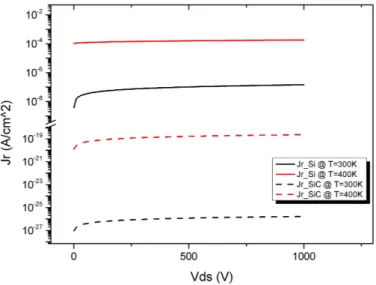
In Figure 1.9, the results from a numerical simulation of the leakage current in reverse polarization are presented for Si and SiC n-MOSFETs, which are drawn with solid-lines and dash-lines, respectively. The breakdown voltage of such devices was sim-ulated before. Simulations were performed at 300K (black lines) and common operating temperature of 400K (red lines). It is worth noting that jr depends strongly on the
tem-perature, and the losses related to this effect can be very high for standards Si devices (for the simulation case, it will be ∼ 0.18 W.cm−2 at 125°C). On the other hand, the leakage current of SiC devices is relatively lower at low temperatures; and even when it increases for high temperatures, the jr remains always lower than that for Si at normal
operation temperatures.
Furthermore, when the reverse voltage applied to the drain-source terminals of a MOSFET is close enough to the Breakdown Voltage BV, a process of impact ionization starts due to the high electric field applied. In fact, every electron generated is acceler-ated inside of the crystal structure of the pn-junction, by the effect of the strong electric field imposed, and causes the generation of another electron-hole pair that is known as impact ionization. Such electron and hole generated are again attracted and accelerated by the electric field repeating this cycle, described in the band diagram of the Figure
1.10. Such a process is known as Avalanche Multiplication and enhances the reverse leakage current.
Indeed, this avalanche multiplication is very complex, and several models exist ac-cording to the technology and application of interest, which define an avalanche multi-plication factor (M) [32], [33]. In our case, different considerations must be performed for avalanche multiplication factors due to the electron, holes and space charge currents (Mn,p,sc). However, good approximations can be performed using the relation expressed
by [34] as:
M = 1
1 − (Vr
BV)m
(1.28) where, the fitting exponent m ranges between 4 and 6. We have considered m = 5 for Si and SiC simulation using jr= M (js+ jsc). The enhanced jrcurrents obtained for Si and
Figure 1.9: Simulation results of jr in function of VDS for a Si (solid-lines) and SiC
(dash-lines) of an n-MOSFET designed for BV=1 kV. Simulations performed at 300K (black-lines) and 400K (red-lines). Avalanche multiplication effect during the breakdown was not considered.
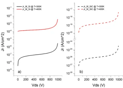
SiC n-MOSFETs are drawn in Figure 1.11a and 1.11b, respectively. It is worth noting that jr currents grow rapidly during the low regime reverse voltage than those presented
in Figure1.9. Then, the jrcurrents rise slightly while the reverse voltage becomes high.
Finally, they increase suddenly again with the high reverse voltage regimes closely to the breakdown voltage. However, the leakage current in SiC device keeps on lower values than those for Si device, even when the temperature grows to 125°C.
1.3.3 On-Resistance Parameter
Another main aspect to care in power semiconductor devices is the drain to source on-resistance (RDSon) value during the conductive regime. While for low current and voltage applications, transistors present considerable high on-resistances; for high current densities applications, low values of on-resistance are required to avoid self-heating and losses due to power dissipation. In the Figure 1.12, the resistance contribution of every section inside a vertical power MOSFET structure forming the total resistance path, is represented. Such resistance contribution can be expressed as:
RDSon = Rsp+ Rn++ Rch+ Ra+ Repi+ Rsub (1.29)
where, Rsp is the resistance in between source contact and package terminal, Rn+ is the
source region resistance, Rchis the channel resistance, Rais the resistance related to the accumulation region, Repiis the epitaxial resistance and Rsubis the substrate resistance close to the drain terminal.
Figure 1.10: Band diagram’s example of the interaction of electron-hole generation by impact ionization in the depletion zone during avalanche multiplication under the effect of a strong electric field.
Figure 1.11: Simulation results for jr in function of VDS for a) Si and b) SiC
n-MOSFETs designed for BV=1 kV. Simulation performed at 300K (black-lines) and 400K (red-lines). Avalanche multiplication effect during the breakdown was considered.
Figure 1.12: Representation of current path and resistance contribution of different sections in a standard vertical MOSFET.
Table 1.5: Resistance contribution for RDSon standard vertical MOSFET for high
blocking voltage. Values extracted from [35]
Abbr. Section inside Power MOSFET For BV = 600 V (%)
Rsp Package 0.5
Rn+ Source region 0.5
Rch Channel 1.5
Ra Accumulation region 0.5
Repi Epitaxial (drift) region 96.5
Rsub Substrate close to drain terminal 0.5
However, in vertical power MOSFETs, the epitaxial resistance Repirelated to the low
doped drift region has a big contribution in the total resistance between drain-source terminals, as summarized in Table 1.5, because the surface resistances contribution de-creases with the increase of the cell density, which is given by [11]:
Repi=
wD
qµnNDA
(1.30) where, µn is the electron mobility and A is the active area of the device in cm2.
Through a first glance at 1.30, it can be concluded that to reach lower resistances contribution of the epitaxial (drift) region, the ND should be as high as possible due
to Repi is inversely proportional to the doping density. But, Repi is also proportional to the wD and this is in strongly dependence of the semiconductor material electronic properties and the doping density of the drift region as shown in1.18. Moreover, the BV
(a) Results for Si n-MOSFET.
(b) Results for a 4H-SiC n-MOSFET.
Figure 1.13: Numerical calculation of Epitaxial Resistance (Repi) scaled by the active
area (A) of a power MOSFET in function of ND. For comparison purpose, the results simulation for wD and BV are also plotted. Simulations performed at 300K.
is directly proportional to the wD through1.16. This means that for a given high ND, a
decrement of the wD is necessary to reach lower Repicontribution. However, using1.16, the decrement of the wD (or a higher ND using 1.17) sets a lower BV capability. These affirmations are demonstrated by the simulation results presented in Figures 1.13a and
1.13b for Si and 4H-SiC MOSFET devices, respectively.
Figure 1.14: Comparison of Repi, scaled by the active area A, obtained from numerical
simulation for a Si and 4H-SiC vertical power MOSFET in function of ND.
as demonstrated in the last sections. For instances, the BV values obtained though simulation as a function of the ND for a 4H-SiC n-MOSFET, and its respective wD, at a
given ND were shown in Figure1.13b. These values are one order higher than those for a
Si n-MOSFET shown in Figure1.13aincluding the Repiresistance. A direct comparison between the SI and 4H-SiC Repi simulation results obtained is presented in Figure1.14.
It is worth noting that resistance data are scaled by the active area A of the devices. As mentioned, it seems that Repiof the 4H-SiC device has higher values than that of Si ones for the same doping density ND. However, this higher Repi is contrasted with the
higher BV reached for 4H-SiC MOSFET device.
For instance, observing the Figure1.13a, a Si device designed for a BV =1 kV needs a ND=1.83 ×1014 cm−3, which results in wD=85 µm and RepiSi = 210 mΩ.cm
2. On the
other hand, , observing the Figure1.13b, to reach the same BV for a 4H-SiC device is necessary a higher doping concentration ND=2.65 ×1016cm−3, which results in a thinner wD=6.37 µm and RepiSiC = 150 µΩ.cm
2. In this way, 4H-SiC devices demonstrate to
have smaller Repi than Si devices at a same BV without taking in consideration the
impact of the active area (A) factor for each device technology.
1.3.4 Gate Leakage Current
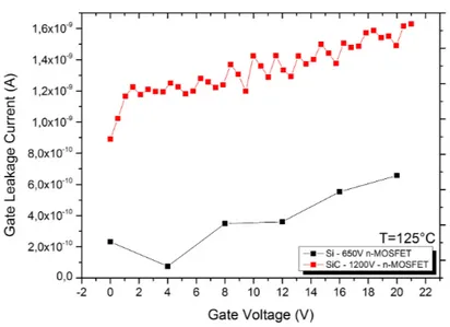
As shown in Figure 1.4, the gate contact terminal in the vertical power MOSFET structures is electrically isolated from the substrate and channel by a dielectric layer. In this way, a potential applied to the gate terminal generates an electric field, which creates a depletion region on the channel. Since many decades, the SiO2 has been preferred in Si technology because it can be easily obtained via thermal oxidation technique. Even if this
Figure 1.15: Comparison of gate leakage current measured on a 650V Si and a 1200V SiC n-MOSFET devices at 125°C.
approach is maintained for SiC, improvements of oxidation techniques and new dielectric materials are also in the course of reducing the considerable presence of interface states [36], [37].
The importance of the gate oxide is related to two tasks: a) Provide a high input impedance for the control gate terminal and b) Facilitate the control of current flow through the channel. Leakage current from gate oxides in power MOSFET devices can reveal defects and drawbacks, which can limit the performance of power MOSFETs. Main limitations of gate oxides performances are related to oxide breakdown, charge tunneling, trapping and interface defects among others. Such limitations are reflected on the gate leakage current as shown in Figure1.15. In this case, the gate leakage current (IGSS) was measured for comparison purpose in two power MOSFETs. The first device was a Commercial On The Shelf (COTS) 650V n-MOSFET in Si and the second device was a R&D 1200V n-MOSFET in SiC. It is evident that improvements are needed in the SiC device manufacturing to decrease its gate leakage current.
Contrary to the nanoscale implementation of MOSFETs, which are integrated into digital and logic integrated circuits, the problematic of gate oxides in power devices are reduced due to the oxide thickness, which must endure high drive voltages (5-20 V) compared with that of nanoscale devices, but maintaining oxide capacitances as low as possible. More details about gate leakage current, models, and tunneling problematics can be found in [38]–[42]
1.3.5 Threshold Voltage Parameter
The threshold voltage parameter is one of the main important parameter to char-acterize the metal-insulator-semiconductor stack in a MOSFET device. As mentioned
where Cox = εox/tox, and it is the specific oxide capacitance.
Only when the device enters in strong-inversion operation, the carrier density be-comes sufficient to allow conduction of current between drain and source terminals through the channel. Hence, the Threshold Voltage (Vth) can be defined as the gate voltage at which the MOSFET enters in the strong-inversion operation. Normally, this condition is reached when surface potential (ψS) is equal to twice the bulk potential
(ψB) [1], [43]. Then, using (1.31) and (1.32), the Vth can be expressed as Vth= QS Cox + 2ψB, (1.33) with ψB= kT q ln( NA ni ). (1.34)
Due to the QS depends on the surface potential ψS and acceptor doping density NA of the p-base region in a n-channel MOSFET, the total charges in strong-inversion
operation are determined in [43] as: QS=
p
4εSqNAψB, (1.35)
where, εS is the electric permittivity of the semiconductor surface. Therefore, a more
defined expression for Vth can be found replacing (1.35), and Cox = εox/tox, in equation
(1.33), as: Vth= tox εox p 4εSqNAψB+ 2ψB. (1.36)
Nevertheless, the expression (1.36) describes an idealized threshold voltage and it does not consider the flat-band voltage (Vf b) of the MOS structure. The Vf bdepends on the charge trapping and impurities ions in the oxide [44], [45], and its study is outside of this work.
However, equation1.36shown that threshold voltage Vthdirectly dependences on the acceptor doping concentration NAin the channel region and the thickness of the dielectric
![Table 1.1: Collection of mobilities reported in literature. Work µ n µ p Technology [cm 2 /V.s] [cm 2 /V.s] Lutz et al](https://thumb-eu.123doks.com/thumbv2/123dokorg/2875339.9782/35.892.226.663.271.504/table-collection-mobilities-reported-literature-work-technology-lutz.webp)