ALMA MATER STUDIORUM
-
UNIVERSITÀ DI BOLOGNA
Scuola di Scienze
Dipartimento di Fisica e Astronomia
Corso di Laurea in Fisica
P
IEZOELECTRIC
F
ORCE
M
ICROSCOPY
STUDY ON
Z
INC
T
IN
O
XIDE
N
ANOWIRES
Relatore:
Prof. ssa Beatrice Fraboni
Presentata da:
Klein Tahiraj
Correlatore:
Dott. Tobias Cramer
Për mamin
dhe babin.
Sommario
Piezoelectric force microscopy study on zinc tin oxide nanowires
Di Klein TAHIRAJ
I sensori autoalimentati potrebbero trovare un'ampia applicazione per monitorare la salute per-sonale, le automobili o gli edifici. Una delle forme più onnipresenti di energia su cui questi dispositivi potrebbero fare affidamento è l'energia vibrazionale. Per convertire questa energia in energia elettrica, la ricerca si sta concentrando sui materiali piezoelettrici. Esempi di questi materiali, sono gli ossidi di zinco-stagno (ZTO). Questi ultimi, modellati in nanofili e incorpo-rati in un elastomero di silicio presso i laboratori dell’Università di Lisbona, hanno dimostrato di produrre una conversione energetica macroscopicamente efficiente. In questo lavoro uso la Microscopia a Forza Piezoelettrica per caratterizzare la risposta piezoelettrica di un singolo nanofilo di ZTO, cioè per misurarne componente 𝑑33 del tensore di deformazione piezoelettrica.
Il P(VDF-TrFE) in film sottile, ovvero un materiale con proprietà piezoelettriche ben caratte-rizzate, viene utilizzato per calibrare la sensibilità dello strumento. Il valore che ottengo per il 𝑑33 del nanofilo di ZTO è 23.70 ± 0.04𝑝𝑚/𝑉. Una caratterizzazione per un nanofilo ZnO viene
inoltre effettuata con l’obiettivo di usarla come riferimento. Il valore che ottengo è di 10.36 ± 0.03𝑝𝑚/𝑉. Il valore per il nanofilo di ZTO risulta dunque essere circa il doppio di quello dello ZnO. Questo risultato certifica i nanofili di ZTO come buoni candidati per la conversione di energia nei futuri dispositivi autoalimentati.
Abstract
Piezoelectric force microscopy study on zinc tin oxide nanowires
by Klein TAHIRAJ
Self-powered sensor devices could find widespread application to monitor personal health, au-tomobiles or buildings. One of the most ubiquitous form of energy on which these devices could rely is vibrational energy. To convert this energy into electrical energy, the research is focusing on piezoelectric materials. Examples of these materials are ZnO or Zinc Tin Oxides (ZTO). Modelled into nanowires and incorporated into an elastomer at the University of Lisbon, these materials have been demonstrated to result in macroscopically efficient energy conversion. In this work, I use Piezoelectric Force Microscopy to characterize the piezoelectric response of a single ZTO nanowire, namely, to measure the component 𝑑33 of its piezoelectric strain tensor. P(VDF-TrFE) thin film, i.e. a material with well characterized piezoelectric proprieties, is used to calibrate the instrument sensitivity. The value I obtain for the 𝑑33 of the ZTO nanowire is
23.70 ± 0.04𝑝𝑚/𝑉. In order to use it as a reference, I perform a characterization also to a ZnO nanowire. The value I obtain is 10.36 ± 0.03𝑝𝑚/𝑉. The value for the ZTO nanowire is there-fore about double that of the ZnO. This result certifies ZTO nanowires as good candidates for energy conversion in future self-powered devices.
Table of Contents
Introduction ... 1
1
Chapter 1 – Theoretical Background ... 3
1.1Theoretical Notions ... 4
1.1.1 Dielectrics and Electric Polarization ... 4
1.1.2 Piezoelectricity ... 7
1.2Piezo-materials ... 9
1.2.1 Piezo polymers: PVDF and P(VDF-TrFE) ... 9
1.2.2 Piezo-ceramics: ZnO and ZTO ... 11
1.2.3 Major applications. ... 12
2
Chapter 2 – Instrumental Set Up and Techniques ... 15
2.1Techniques ... 16
2.1.1 Contact-Mode ... 16
2.1.2 Non-Contact Mode ... 17
2.1.3 Electrostatic Force Microscopy (EFM) ... 19
2.1.4 Piezoelectric Force Microscopy (PFM) ... 20
2.2Cantilever selection ... 22
2.3Sample Manufacturing ... 23
3
Chapter 3 - Samples Analysis and Discussions ... 25
3.1P(VDF-TrFE) ... 25
3.2ZnO ... 34
3.3ZnSnO3 ... 37
Conclusions ... 41
1
Introduction
Self-powered sensor devices could find widespread application to monitor personal health, au-tomobiles or buildings, providing information that could help to improve our security and well-being as well as to reduce our environmental impact1,2. Self-powered sensor devices rely on an energy source other than batteries or power cords. With the appropriate technologies, energy from chemical reactions, but also from thermodynamic or mechanic processes, can be converted into electrical energy. One of the most ubiquitous forms of energy to be harvested by self-powered devices is vibrational energy. Indeed, our world is constantly affected by continuous vibrations and motions. The ground, for example, even if it is not easily perceived, vibrates constantly3. Also, the sounds that we hear, are nothing more than vibrations of the fluids that surround us. Thus, the human body is also continuously affected by vibrations and motions. The ability to transform mechanical vibrational energy into electrical energy is what can open the door to the new technologies of the future. One of the best-performing methods for obtaining energy from vibrations is to exploit the phenomenon of piezoelectricity. The deformation of a piezoelectric material is proportional to the electric field applied, and vice versa. In the general case, this proportionality is expressed by a tensor. The magnitude of the tensor elements then describes the efficiency of a material for electromechanical energy conversion. In recent years it has been demonstrated that nanostructured piezoelectric materials have particularly large pi-ezoelectric coefficients and can be tailormade to be included in soft pipi-ezoelectric composites for energy-harvesting devices4–7. An example are ZnO or 𝑍𝑇𝑂 − 𝑏𝑎𝑠𝑒𝑠 nanowires incorporated into a silicone elastomer as fabricated in recent progress at the University of Lisbon. Such ma-terials have been demonstrated to result in macroscopically efficient energy conversion able to power small LEDs8. However, a detailed characterization of the piezoelectric response of the
single nanomaterial is still missing and is crucial to understand the operation mechanism and performance of the energy harvester. In this work, I will address this task by performing piezo-electric force microscopy on ZnO and 𝑍𝑛𝑆𝑛𝑂3 produced in the laboratories of the Materials Science department of the NOVA University of Lisbon. The objective is to determine the d33 element of the piezoelectric tensor of single nanowires.
In Chapter 1, an introduction to the phenomenon of piezoelectricity is presented. Starting from its discovery in 1880, we describe first the properties of dielectrics, of which piezoelectric
2
materials are a subclass, and then we offer an explanation of the phenomenon of piezoelectric-ity. Then the material to be characterized and the two used as reference standards. ZnO is a material of the same class of the 𝑍𝑛𝑆𝑛𝑂3and is therefore used as a comparison. PVDF-TrFE,
on the other hand, has been studied for a long time and its piezoelectric properties are well known. Therefore, it is used as an absolute reference for the calibration of the instrument used for measurements. Finally, a more complete presentation of the applications of 𝑍𝑛𝑆𝑛𝑂3 and
ZnO is presented. In Chapter 2, the equipment used for the measurements is described, i.e. the
NX10 Scanning Probe Microscope of the Park System Corp. Starting from a general description of its functioning, the main techniques that will be used for the characterization of the various materials are then explored. Chapter 3, on the other hand, is dedicated to the discussion of the data collected. Starting from the images reworked with Gwydionn, the piezoelectric properties of PVDF-TrFE are first verified. Then, fixing the value of the 𝑑33 of the latter to that known from the literature, the value of the sensitivity of the instrument is calculated. Then we move on to the characterization of the piezoelectric properties of the 𝑍𝑛𝑆𝑛𝑂3 and ZnO calculating the value for their 𝑑33. At the end, in the conclusion part, we compare the obtained 𝑑33 values and resume the whole work.
3
1 Chapter 1 – Theoretical Background
Piezoelectricity is the accumulation of electric charge on a solid material’s surface in response to a mechanical stress. Its first observation was made in 1880 by the French physicists Jacques and Pierre Curie, who demonstrated that pressure on quartz and topaz crystals produces electric currents9. Today the definition also includes the deformation of certain solids under the influ-ence of an external electric field. This latter phenomenon is precisely called the inverse
piezo-electric effect and was deduced mathematically from thermodynamic principles by Gabriel
Lippmann in 18819. Figure 1.1 shows a schematic diagram of the piezoelectric effect10. The term piezoelectricity arises from the analogy with the earlier know phenomenon of ferroelec-tricity, where the prefix piezo- is borrowed from the Greek word πιέζειν (piezein), which means to press9. Piezoelectric materials present a broad set of electromechanical proprieties that lead to interesting applications. For instance, historically one of the first applications was an ultra-sonic submarine detector, developed by the French physicist Paul Langevin during the World War I11. Nowadays, piezoelectric materials are exploited for a large variety of precision
applications. This applications includes actuators12, pressure sensors13, underwater acoustic14, drug delivery in therapies15 and energy harvesting16. In the following I will provide a detailed introduction on the physical principles underlying the piezoelectric effect.
4
1.1 Theoretical Notions
1.1.1 Dielectrics and Electric Polarization
All piezoelectric materials are a subset of dielectric materials, to understand the proprieties of the former, is so necessary to start from a model of the latter. A dielectric is an electrical insu-lator material that can be polarized by the application of an electric field. When a dielectric material is placed in an electric field, because the covalent bonds are strong enough to keep the electrons in place, it does not exhibit a flow of charges as happens for metals. Indeed, only local displacements of electrons and of the atomic nuclei happen, resulting in a net deformation of the material through the so-called dielectric polarization phenomena. Because of this net formation, the material undergoes change in its dimensions. The magnitude of this change de-pends upon the crystal class to which the dielectric belongs. Among the 32 crystal classes, 21 are non-centrosymmetric, i.e. do not possess a centre of symmetry, while 11 are centrosymmet-ric, i.e. do possess a centre of symmetry. When a non-centrosymmetric dielectric is subjected to an external electric field, because of its structure, the movements of the neighbouring ions lead to significant deformations of the crystal. When this happens, the material is called
piezo-electric. Instead, when a centrosymmetric dielectric is subjected to an external electric field, the
displacement of cations and anions get cancelled because of the symmetric structure. Here, the net deformation is ideally nil. However, because of the anharmonicity of real bonds, a small second order deformation arises. This deformation has the name of electrostrictive effect. It must be said that because all dielectrics have non-perfectly harmonic bonds, the electrostrictive effects affects all of them. This means that also the piezoelectric material undergo the electro-strictive effect, but it get masked by the magnitude of the piezoelectric effect17. A second clas-sification for dielectrics starts from their charge distribution. We call nonpolar dielectrics ma-terials whose centres for positive and negative charges do coincide. Polar dielectrics are instead dielectrics in which opposite charge centres do not coincide. Under the influence of an external electric field, in the former type, the centres of the positive and negative charges get separated and an induced dipole moment is generated, while in the latter the native dipole moment is subjected to a reorientation in the direction of the field.
Taking into account only electrostatic interactions, atoms and molecules can be described by an electric charge distribution 𝜌: 𝜌(𝑥, 𝑦, 𝑧). This distribution is a function of the spatial
5
coordinates and is positive where the nuclei are and negative where the electrons are. The elec-tric field generated by the distribution at distant points can be computed as −𝜵𝜙 . The term 𝜙 is the electric potential of the distribution, namely:
𝜙 = 1
4𝜋𝜖0∫ d𝑣
′𝜌(𝑥
′, 𝑦′, 𝑧′)
𝑅 (1.1)
with d𝑣′ as a volume element of the distribution and 𝜖
0 as the vacuum permittivity. For
non-trivial distributions, the expression of the potential can be obtained from symmetry arguments as a series called multipole expansion18. A general result is that the behaviour of the potential
at large distances from the source will be dominated by the first term of the series whose coef-ficient is not zero18. Looking to multipole coefficients, the first reads as 𝐾0 = ∫ d𝑣′ρ, which is
the total charge in the distribution. Thus, for equal amounts of positive and negative charge, the system results neutral and the 𝐾0 coefficient is null. In this case, the second coefficient deter-mines the behaviour of the potential at large distances. This latter reads as 𝐾1 = ∫ d𝑣′𝑟′𝑐𝑜𝑠𝜃𝜌 where 𝑟′ is the distance of the volume 𝑑𝑣′ from the centre of the distribution and θ is the angle
between 𝑟′ and the axis passing through the centre and the point in which the potential is being measured. A relevant theoretical result is that for neutral charge distributions, the value of 𝐾1
is independent of the position chosen as origin. The quantities 𝐾0, 𝐾1are related to what are called moments of the charge distribution. Specifically, we call the first monopole moment, which is a scalar, and the second a component of the dipole moment of the distribution, which is a vector18. As the expansion of the multipole expansion goes on, more 𝐾-coefficients appear, giving more and more details about the problem, however, for our analysis, only the first two have a crucial role, and here I will provide only an analysis of the 𝐾1. Rewriting 𝑟′𝑐𝑜𝑠θ as the projection of 𝒓′on the direction towards the measurement point, viz 𝒓̂𝒓′, we can express the
contribution of the dipole moment to the potential avoiding the clarification on the origin posi-tion, namely:
𝜙K1 = 𝒓̂ 4πϵ0𝑟2
∫ 𝑑𝑣′𝒓′ρ (1.2)
6
𝒑 = ∫ 𝑑𝑣′𝒓′𝜌 (1.3)
which has the dimensions of 𝑐ℎ𝑎𝑟𝑔𝑒 × 𝑑𝑖𝑠𝑡𝑎𝑛𝑐𝑒.
A simple but illustrative case is when the charge distribution is built by two single opposites punctiform charges q, situated at a distance d from each other. In this case, the expression for the dipole moment can be easily computed as 𝒑 = 𝑞𝑑𝒅̂, where 𝒅̂ goes from the negative to the positive centre of charge. This case can be used to intuitively understand the behaviour of sim-ple molecules and atoms under the influence of an external electric field.
Assuming that the dipole moments of the molecules or atoms composing a material are in the form of 1.3, we define the electric polarization P as the total dipole moment per unit volume, namely:
𝑷 =∑ 𝒑𝑖 𝑖
𝑉 (1.4)
For materials build-up of neutral molecules, only the dipole moments account for the electric field at a large distance. As already stated, whenever an electric field E is applied, the randomly spread dipoles tend to align to its direction, passing from a state of null net polarization to a finite polarization that increases as the external field increases. This process goes on until all the dipoles are coherently aligned to the field, viz when the so-called saturation point is reached. For later convenience we define de displacement field D as the effects of an external electric field E and the related total polarization P within a material, namely:
𝑫 = 𝜖0𝑬 + 𝑷 (1.5)
This latter, in a more general case, can also be written as:
𝑫 = 𝜖𝑬 = 𝜖0𝜖𝑟𝑬 (1.6)
where ϵ, ϵ𝑟 are respectively the absolute and relative permittivity19.
The nature of the piezoelectric effect is closely related to electric dipoles, above described. Moreover, dipoles near each other tend to align in the so-called Weiss domains, which until an external electric field is applied, are collectively randomly oriented20. If the applied electric
7
field is large enough, the process of poling happens, i.e. the dipoles orient themselves perma-nently along the direction of the field. The tendency of a material to change its polarization is called electric coercivity. The higher it is, the higher must be the field to achieve permanent polarization.
1.1.2 Piezoelectricity
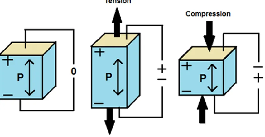
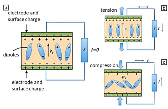
Upon all dielectric materials, piezoelectricity arises only from those whom present non-centro-symmetric crystal structures. When an external strain or pressure is applied, the dipoles in the crystals get oriented from a random configuration to a more coherent one. Furthermore, also the vice versa case can arise. Thus, negative and positive free charges appear on opposite faces of the structure, due to the change of polarization. This represents the basic principle of the direct piezoelectric effect and is summarized in Figure 1.221. On the other hand, the application of an external electric field produces the displacements of the charge centres which leads to a
Figure 1.2 Piezoelectric effect across electrical load. a) No mechanical load, b) compressive load leading to a decrease in polarisation relative to the no load con-dition, c) tensile load leading to an increase in polarisation relative to the no load condition.
8
net deformation due to the consequent dipole reorientations. This latter instead, is the basic explanation for the inverse piezoelectric effect.
At low electric fields and low mechanical stresses, the behaviour of the material can be consid-ered in meaningful approximation as linear. Starting from this, the piezoelectric effect reads as the combination of the displacement field D from 1.6 and the Hook’s law. In tensorial notation, this reads as:
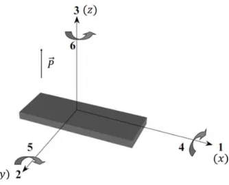
Here, s is the compliance, T the stress S the strain, ϵ the absolute dielectric permittivity and d the matrix of piezoelectric constants. Indexes 𝑖, 𝑗 = 1, 2, 3, 4, 5, 6 and 𝑚, 𝑘 = 1, 2, 3. These fol-low the common practice, exposed in Figure 1.322, in which 1, 2, 3 indicate x, y, z and 4, 5, 6 the shear planes perpendicular to the respective axis22. Meanwhile, the superscripts T and E
highlight that the electric and stress fields are constant across the system.
𝑆𝑖 = 𝑠𝑖𝑗𝐸𝑇𝑗+ 𝑑𝑚𝑖𝐸𝑚 (1.7)
𝐷𝑚 = 𝑑𝑚𝑖𝑇𝑖+ 𝜖𝑖𝑘𝑇𝐸𝑘 (1.8)
9
Varying the indexes, a total of four tensors of piezoelectric coefficients can be obtained. For our investigation, we focus only on the tensor of piezoelectric strain constants 𝑑𝑖𝑗 which reads
as:
The subscripts i, j indicate that the electric field applied, or the collected charge, are in the direction of i for a displacement, or a force, in the direction of j.
Thus, we can mathematically describe the response of the piezo-material to an eternal electric, or force, field. For the sake of this work, our attention is on the component 𝑑33 of the
piezoe-lectric strain constants tensor, which represents the strain in the direction of the z-axis for an electric field applied in the direction of the z-axis, too.
1.2 Piezo-materials
In the last few years many active materials such as shape memory alloys and optical fibres, called nowadays with the popular name of smart materials, have been developed and patented. Among these, stand the piezoelectric materials. These can be divided into two main subsets, ceramics (also including single crystals) and polymers (together with biological compounds). The former, historically represent the first set of materials presenting piezoelectric proprieties. Example of these are quartz, topaz and lead titanate (𝑃𝑏𝑇𝑖𝑂3). Nevertheless, in their more
up-to-date version, piezoelectric ceramics are represented by nanostructures made by inorganic compounds such as ZnO and Zinc Tin Oxids. Piezo-polymers instead, were developed and well-characterized only in the last fifty years, starting from the works of Kawai H. in the early ’7023. Examples of piezo polymers are PVDF, polyamines and polyureas.
1.2.1 Piezo polymers: PVDF and P(VDF-TrFE)
Piezoelectric polymers are nowadays deeply investigated, with a few thousand papers produced per year24. Their proprieties are so different in comparison to inorganics that they are uniquely qualified to fill niche areas where single crystals and ceramics are incapable of performing as effectively25. Even if polymers have a lower piezoelectric strain constant than crystals, they present much higher piezoelectric stress constants; thus, they are much better sensors than
𝑑𝑖𝑗 = (𝜕𝐷𝑖 𝜕𝑇𝑗) 𝐸 = (𝜕𝑆𝑗 𝜕𝐸𝑖) 𝑇 (1.6)
10
ceramics. Moreover, they offer the advantage of processing flexibility, being lightweight and manufactured into large sheets cuttable in any complex shape. The structural requirements that a polymer should meet to be piezoelectric are: (a) the presence of permanent dielectric dipoles in its structure, (b) the ability to align the dipoles under the influence of an external electric field and to maintain this polarization once it’s achieved, (c) the ability to undergo large strains when stressed mechanically25. Among the piezoelectric polymers, the semi-crystalline ones
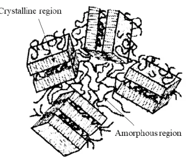
play a major role. These, in order to be piezoelectric, must have a polar crystalline phase, whose degree depends on their method of preparation, dispersed within amorphous regions as shown in Figure 1.425. In these materials the piezoelectricity arises from alignments of the crystals in
consequence of an external stretch; while the inverse
piezoelectric effect arises from the alignment of the crystal phase in the film plane under the influence of an external electric field.
Since the works of Kawai H., polyvinylidene fluoride (PVDF) has been one of the most inves-tigated piezoelectric polymers. Detailed descriptions of its most important proprieties have been described in various reports26’27’28, but among all, what makes it so attractive are its piezoelec-tric, pyroelectric and ferroelectric proprieties due to its spatially symmetrical-disposed
Figure 1.4: Semi-crystalline polymer. Representation of crystal and amorphous re-gions inside a film plane.
11
hydrogen atoms. Moreover, its amorphous phase has a glass transition of −35°𝐶: far below room temperature; this makes it flexible for most of its applications. Furthermore, it has a die-lectric constant about four times greater than most of the other piezo-polymers. After poling, it has excellent polarization stability which however decreases reaching Curie’s temperatures. In addition, PVDF is at least made up by 50 to 60% crystal phase and has at least four crystal phases (α, β, γ , 𝑎𝑛𝑑 δ), three of which are polar.
On the other hand, another piezo-polymer which in the last years has gained the attention of the scientific community is a copolymer of PVDF, namely the poly(vinylidene fluoride-trifluoro-ethylene) (P(VDF-TrFE)). Because of its predominantly crystallization in the β phase, it pre-sents strong piezoelectric features, together with pyroelectric and ferroelectric ones. Its struc-ture is basically the same as the PVDF with the further insertion of PTrFE. Compared to its homopolymer, PVDF-TrFE presents a much larger crystal phase, up to 90%, thus it exhibits stronger piezoelectric effect and has a higher remnant polarization. Moreover, in the form of single-crystalline film, its 𝑑33 has reached, in later studies, values of about −38𝑝𝑚/𝑉29, which
represents the highest value among synthetic piezo-polymers.
Because of their nice piezoelectric proprieties and their relative low cost of production, PVDF and P(VDF-TrFE) both represent the current state of the art in the field of semi-crystalline piezo-polymers.
1.2.2 Piezo-ceramics: ZnO and ZTO
In addition to piezo polymers, in recent years materials made up by semiconductive oxides have also gained the attention of the scientific community30. ZnO nanostructures have been intensely investigated because of their flexibility in numerous applications. Indeed, they carry the ad-vantages of semiconductive materials together with the piezoelectric proprieties of ZnO2 which originate within its atoms and is repeated throughout the solid due to its high crystallinity6. Moreover, depending on the doping, ZnO has also a wide-bandgap semiconductivity, high transparency, high conductivity room temperature ferromagnetism and chemical sensing ef-fects30. Also, it can be easily integrated with flexible substrates and because of its low cost of
production, together with its non-toxicity, it’s a good candidate for the technologies of the fu-ture. Unfortunately, applications have been restricted by the low electric power output achieved
12
with the ZnO nanostructures31. For instance, because of a high free carrier density, a piezoelec-tric potential screening effect is induced, preventing the manufacturing of stable and large power performances. However further investigations have found that improvements of the power generating of the ZnO nanostructures can be achieved controlling the defect and free charge carries throughout thermal annealing treatment, doping and hybridization with poly-mers32.
On the other hand, it has been a recent trend to move from single to multicomponent oxides. The multicomponent Zinc Tin Oxide 𝑍𝑛𝑆𝑛𝑂3 presents numerous exploitable proprieties. For instance, both zinc and tin are abundant and recyclable, but also, being a ternary oxide, its pro-prieties can be tuned adjusting the cationic ratio. Moreover, different shapes can be achieved depending on the production process, and in addition 𝑍𝑛𝑆𝑛𝑂3also crystallizes in both
rhombo-hedral and orthorhombic structures33. 𝑍𝑛𝑆𝑛𝑂3 structures such as nanocubes, microbelts and nanoplates have been shown to manifest piezoelectric and piezoresistive effects, this qualifies 𝑍𝑛𝑆𝑛𝑂3 as a potential material for future energy harvesting devices34’35. 𝑍𝑛𝑆𝑛𝑂3 structures that were used for this work were nanowires produced by hydrothermal precipitation in a con-ventional oven. Although, to verify the efficiency of their proprieties as piezo-materials, a char-acterization of their 𝑑33 value must to be done. This will be the aim of the Chapter 3.
1.2.3 Major applications.
As stated, piezoelectric materials can be employed in many applications. One of the applica-tions on which research is focusing the most, is that of energy harvesting structures, i.e. those nanostructures capable of producing energy from small mechanical stresses. Indeed, devices such as pacemakers could be self-powered, if able to extract their own energy from the numer-ous potential energy sources of the human body, such as the mechanical energy of the muscular movements or blood pressure, or the vibrational energy in the form of acoustic. One of the most promising materials are non-centrosymmetric oxides, which have been taken into account in the last few years because of their spontaneous polarization proprieties, i.e. the starting point for technologies that rely on piezoelectricity. Therefore, ZnO and 𝑍𝑛𝑆𝑛𝑂3 nanostructures have
13
can be generated, leading to applications to devices of many fields, such as self-power gener-ating systems for medical issues, wearables, sensor, actuators and wireless technologies.
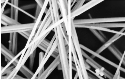
One of the most exploited nanostructures for these aims are nanowires. These nanostructures are defined as structures that have a thickness constrained to tens of nanometres and an uncon-strained length. Because of these scales, they can be considered as one-dimensional materials. In addition, due to the laterally quantum confinement of the electrons in nanowires, these man-ifest proprieties that have not been observed in three-dimensional materials. An example of nanowires is provided in Figure 1.536.
Figure 1.6: Working principle of a flexible substrate-base nanogenerator. a) Sche-matic diagram of the structure without mechanical deformation, b) Demonstration of the output scaling-up when mechanical deformation is induced.
14
One of these structures can act like a diode when subjected to mechanical stress, by running the charges to an external circuit under favourable conditions. Moreover, it conducts in one direc-tion only, being ZnO and 𝑍𝑛𝑆𝑛𝑂3 both semiconductors37. So, the integration of many
coher-ently oriented nanowires could lead to an enough power supply for such devices. Possible nan-ogenerators made up by nanowires are for instance: fibres-based38, hard substrate-based39, flex-ible substrate-based40 as shown in Figure 1.64.
Although, many other materials apart from ZnO and 𝑍𝑛𝑆𝑛𝑂3also manifest strong piezoelectric proprieties that can be exploited for energy harvesting, thus, in order to evaluate their effective-ness analysis on their 𝑑33, must be done. The value for the ZnO has been already well docu-mented in literature41, nevertheless a further value assessment will be done in Chapter 3, in order to use it as a reference for the value of 𝑍𝑛𝑆𝑛𝑂3 which instead hasn’t yet a quantitative characterization.
15
2 Chapter 2 – Instrumental Set Up and Techniques
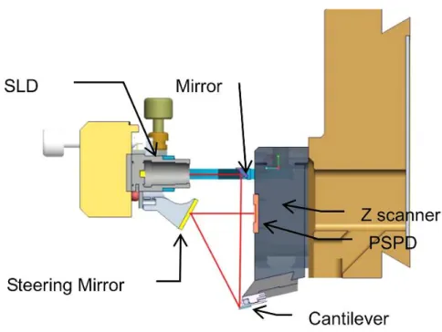
Atomic Force Microscopy (AFM) is a method used to determine the three-dimensional shape of a surface with sub nanometre resolution. The surface morphology is not investigated in the usual way, i.e. by reflections or shadows. Rather, each point within the provided 2D array rep-resents a measurement of surface height, made using a sharp solid force probe. The basic func-tioning of the AFM is simple Its basic set up is shown in Figure 2.142. A cantilever with a very sharp tip slides over the surface of the sample. Different operation modes, that will be later explored in their details, can be selected. As the tip approaches, it interacts with the surface throughout various forces, for example Van der Waals or electrostatic forces. Due to the impact of such forces, the tip cantilever is deflected. Cantilever deflection is measured by an SLD beam that is centred at on the cantilever and reflected into a position-sensitive photodiode (PSPD). In typical operation modes a feedback-loop-height control maintains the tip-cantilever interactions at constant setpoint by moving up or downwards the tip-cantilever system. Tracking the changes in cantilever height allows at the end to reconstruct the three-dimensional representation of the surface.
16
By introducing modulation techniques, atomic force microscopy enables to distinguish the dif-ferent forces acting on the cantilever and many other measurements can be performed beside the simple morphology. Thus, Atomic Force Microscopy results as a versatile microscopy tech-nology to study samples at nanoscales. In my work, I used NX10 Scanning Probe Microscope of the Park System Corp.
2.1 Techniques
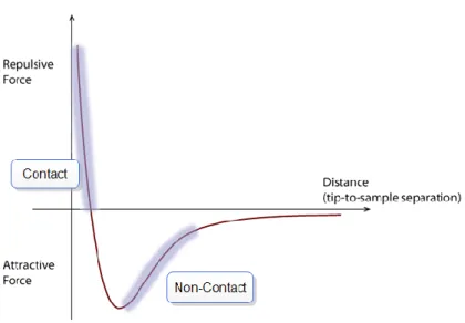
2.1.1 Contact-ModeOperating in contact mode implies that the tip makes a soft physical contact with the surface of the sample. The system made up by the tip attached to the cantilever has a spring constant lower than the one of the atoms of the sample. Because of this, as the tip touches the surface, the interaction force is more likely to deflect the cantilever, rather than deform the sample. However, when the cantilever reaches its maximum deflection, a deformation of the sample can happen. So, the cantilever gently traces the sample bending under the effect of the contact forces. A more detailed analysis of the physical scenario is done by taking into account the Van der Waals forces42. As the tip approaches the surface, their atoms get first weakly attracted. This interaction goes on until the reciprocal distance is so little that their electronic clouds start to repel each other due to electrostatic forces. Therefore, further decrease in the distance leads to the weakness of the attractive component of the Van der Waals forces, that goes to zero when atoms are at apart about the length of an atomic bond. Then, when the Van der Waals forces become positive, i.e. repulsive, the atoms are in contacts. Because of the steepness of the Van der Waals force in the repulsive region, any force that attempts to push the atoms closer gets almost entirely balanced. Therefore, any attempt of the cantilever to penetrate the surface of the sample is instead turned into deflections. So, increasing the force is more likely to cause the deformation of the surface, rather than a closer contact. A basic representation of the Van der Waal forces is provided in figure 2.243.
17
The position of the cantilever is tracked with optical techniques. As stated, the movements are collected as the movements of an SLD light beam centred on the cantilever by a PSPD. This latter can measure displacements of light in the order of 10Å𝑚; furthermore, because of the ration of the path length between it and the cantilever and the length of the cantilever itself, the system can detect sub-angstrom movements, due to the resultant mechanical amplification. Once the deflection is detected, it is used as an input to a feedback-loop circuit. Consequently, the z-servo is moved in order to restore the SLD beam on its setpoint on the PSPD; thus, the force between the tip and the sample is maintained constant. The resulting image is so generated from the motion of the z-scanner. Trough this technique, be can measure simultaneously topog-raphy and other characteristic, such as friction forces, spreading resistance and piezoelectric proprieties. However, Contact-Mode presents several disadvantages. For instance, soft samples can be destroyed by the tip and also this latter is consumed by the rubbing. Moreover, speed scanning must take into account the feedback-loop and its response time, ; thus, leading to longer acquisition times compared to other modalities44.
2.1.2 Non-Contact Mode
Relying on the spatial shape of the Van der Waals forces allows further methods of investiga-tion. In Non-Contact AFM the cantilever does not touch the surface of the sample, instead, it
18
vibrates at its resonant frequency over it. In this operation mode, the space between the two structures is about 1 − 10Å. In contrast with Contact Mode, which relies on repulsive forces, the Non-Contact Mode measures topography throughout the attractive ones. Consequently, the force between the tip and the sample is very low; thus, a direct measurement of its variation is very difficult to achieve. In NCM, one detects the slight changes that the attractive surface forces induce to the vibration phase or the vibration amplitude of the cantilever.
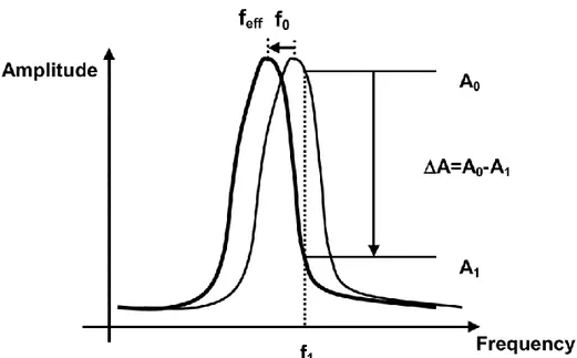
The first step is to determine and fix a value for the resonance frequency 𝑓0 of the cantilever. This is done by driving the cantilever vibration with a bimorph at a fixed amplitude and varying the frequency until the resonance phenomenon occurs. Then, it has to be considered that, as the tip vibrates, its interaction with the surface changes its intrinsic spring constant 𝑘0. As the sys-tem tip-sample-force can be modelled as a forced harmonic oscillator and the resulting effective value for the spring constant 𝑘𝑒𝑓𝑓 is defined through the following relation:
𝑘𝑒𝑓𝑓 = 𝑘0−𝜕𝐹(𝑧)
𝜕𝑧 (1.1)
Figure 2.3: oscillation amplitude vs frequency in a neighbourhood of the resonance fre-quency
19
As the value 𝑘𝑒𝑓𝑓 changes, also does the value of the resonance frequency, leading to a new
value 𝑓𝑒𝑓𝑓. Indeed, the following relation holds:
𝑓𝑒𝑓𝑓 = √
𝑘𝑒𝑓𝑓
𝑚 (1.2)
where m is the mass of the cantilever. As shown in Figure 2.342, vibrating the cantilever at a
frequency 𝑓1, for instance, a little larger than 𝑓0, a little shift to 𝑓𝑒𝑓𝑓 leads to a large change in amplitude. This large change is due to the steepness of the frequency vs amplitude graph in a neighbourhood of the resonance frequency. Therefore, is possible to relate the amplitude change Δ𝐴 measured in 𝑓1 to the height change Δ𝑑, namely the distance between the probe and the surface. Then, as the change in amplitude is measured, a feedback loop compensates the result-ing change in distance usresult-ing the z-stage. The topography image is build maintainresult-ing constant the amplitude 𝐴0 and the distance 𝑑0. Moreover, the difference between the amplitude
oscilla-tion and its set point, is what we refer as Non-Contact Mode Error Signal (NCM Error Signal)
2.1.3 Electrostatic Force Microscopy (EFM)
In most investigations, the simple topography image is not enough to well characterize a mate-rial. For instance, topography doesn’t contain information about the electric or piezoelectric proprieties. Nevertheless, various techniques perform this task. The Non-Contact EFM is one of these. Proprieties such as the surface potential and the charge distribution are obtained by applying a bias to the tip and measuring the deflections of the cantilever under the electrostatic forces that arise. The most refined EFM technique is the so-called enhanced one which relies on a lock-in amplifier42. This latter fulfils two tasks: on one hand, it applies to the tip an AC bias of a frequency 𝜔, whereas on the other it separates this latter frequency to the output signal. Indeed, the signal obtained by the enhanced EFM consists in both surface topography and elec-trical proprieties generated by the Van der Waals and electrostatic forces respectively, and the key of the effectiveness relies on the ability to separate these signals. Taking into account also the possibility to apply a DC bias to the sample base, the overall expression for the electromag-netic potential that arises in the system is given by:
20
𝑉(𝑡) = 𝑉𝐷𝐶− 𝑉𝑠+ 𝑉𝐴𝐶𝑠𝑖𝑛𝜔𝑡 (2.3)
where 𝑉𝐷𝐶 is the potential to the sample base, 𝑉𝑠 is the native surface potential of the scanned area, and 𝑉𝐴𝐶 and 𝜔 are respectively the amplitude and the frequency of the external AC voltage. Modelling the system as a parallel plate capacitor model, the equation for the dynamic, taking into account also equation 2.3, reads as:
𝐹(𝑡) =𝐶 × 𝑉 2 𝑑 = (2.4) = 𝐶 𝑑{(𝑉𝐷𝐶− 𝑉𝑆) 2+ 2(𝑉 𝐷𝐶− 𝑉𝑆)𝑉𝐴𝐶𝑠𝑖𝑛𝜔𝑡 + 1 2𝑉𝐴𝐶 2 (1 − 𝑐𝑜𝑠2𝜔𝑡)} (2.5)
Here F is the electrostatic force acting on the tip and C the capacitance of the system. Starting from Equation 2.4, the signal can be analysed in terms of its three separate parts. Indeed, DC deflection can be read directly from the software and the AC signals can be read by the lock-in system, which can read either the part with a frequency of 𝜔 or 2𝜔. These latter, contain re-spectively information about the surface charge and the surface capacitance gradient (viz d𝐶/d𝑧). In conclusion, applying an AC bias with a frequency 𝜔 to a tip oscillating with a fre-quency 𝑓 over a surface, two interactions arise: the electrostatic one and the Van der Waal’s one. From this, using precise and different values for the frequencies 𝜔 and 𝑓 is possible to extract both information about topography and electrostatic proprieties. Usually the frequency ω of the AC bias is of 17𝑘𝐻𝑧; whereas f is chosen accordingly to the cantilever proprieties.
2.1.4 Piezoelectric Force Microscopy (PFM)
Piezoelectric Force Microscopy investigates the electromechanical proprieties of a material. In this technique, a conductive tip is in contact with the surface of the sample and an AC bias is also applied. The AC bias has a frequency ω of 17𝑘𝐻𝑧 as for the EFM. Because of the bias, an electric field arises between the two surfaces. Therefore, if the investigated material is piezoe-lectric, its surface will start to oscillate because of the inverse piezoelectric effect. Instead, os-cillations due to varying electrostatic forces from Equation 2.5 are suppressed due to strong contact forces. This is fundamental in order to acquire high-quality PFM data. From the theory
21
of Chapter 1, we know that the strain 𝑆𝑗 developed in a piezoelectric material is proportional to
the applied external electric field 𝐸𝑖 by the piezoelectric coefficient 𝑑𝑖𝑗. This relation reads as:
𝑆𝑗 = 𝑑𝑖𝑗𝐸𝑖 (2.6)
where the indices follow the convention of Figure 1.3. Assuming that the strain and the field in the longitudinal direction are expressed as:
𝑆3= Δ𝑧/𝑧0 (2.7)
𝐸3 = 𝑉/𝑧0 (2.8)
where 𝑧0 is the thickness of the sample, the so-called longitudinal piezoelectric constant, viz
𝑑33, can be determined by measuring the z-displacement along the field applied in the z-direc-tion, namely:
Δ𝑧 = 𝑑33𝑉 (2.9)
If the initial polarization of the investigated Weiss domains is perpendicular to the sample sur-face and parallel to the field, the displacement will be positive. Instead, if the polarization is antiparallel, the displacement will be negative. Under the influence of the AC bias, the displace-ment of the surface reads as:
where φ is the difference in phase between the applied voltage and the acquired signal. This latter phenomenon is due to the coupling of the AC field with the internal electric field caused by induced orientation of the dipoles. For instance, if the field and the bias are parallel φ = 0; instead, if they are anti-parallel φ = π. This oscillation is then filtered by the lock-in amplifier and used to determine the polarization direction of the sample together with the magnitude of the displacement. Thus, PFM amplitude together with PFM phase are acquired42. To avoid the permanent switching of the domains, a bias lower than the coercive value is applied. Neverthe-less, it has to be said that, for most of the real cases, the studied samples contain randomly oriented polycrystalline structures whose lateral components of the 𝑑𝑖𝑗 are not null. Thus, the vertical response of the sample to the vertical electric field is no longer proportional to the 𝑑33
Δ𝑧 = 𝑑33𝑉𝐴𝐶𝑐𝑜𝑠(ω𝑡 + φ)
22
alone, but also to 𝑑31 and 𝑑15. However, this eventuality will not be taken into account in the
present work.
Piezoelectric Force Microscopy can be used both for global and local mapping of the proprieties of the material. In the latter case, also a DC bias to the sample base is usually connected in series with the AC one to the tip. For large enough DC biases is possible to polarize permanently the samples. Alternating ON states, in which the DC bias is applied, to OFF states, in which the DC bias is null, it is possible to measure the local polarization loop for the material. This tech-nique is the so-called Switching Spectroscopy.
For the sake of this work, it must be said that Equation 2.9 refers to the ideal case. Indeed, measurements operated with an instrument must consider also the sensitivity S of this latter. Thus, tanking sensitivity into account, Equation 2.9 reads as:
Δ𝑧 = 𝑆𝑑33𝑉 (2.10)
The sensitivity can be measured in two ways. The first is through the built-in features of the instrument. The second is using a standard sample with a well-documented piezoelectric coef-ficient. In this thesis I will follow the second path, using P(VDF-TrEE) as my standard refer-ence.
2.2 Cantilever selection
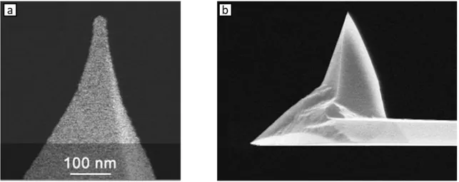
Depending on the technique, several types of cantilevers can be chosen. For instance, in contact mode, is better to choose cantilevers with low spring constants, in order to have a more sensitive response to the differences in level of the surface. Usually, the cantilevers for this technique are also very thin, thus, a lower spring constant can be achieved. When comes to Non-Contact Mode, cantilevers are usually thicker than Contact-Mode, and have a high resonant frequency. Moreover, in order to choose the right cantilever, other parameters such as the coating, and the ratio between the tip radius and the structure that one wants to analyse on the sample. Indeed, the radius of the cantilever should always be lower than the smallest detail of the sample, in order to have the best definition. Furthermore, also the price must be taken in account. Sharper
23
tips are more expansive than thicker ones, also, the damage more often. For my measurements I used different cantilever. For the PVDF-TrFE, a multi75E45 and a NSC36/Cr-Au46. The first one was used for EFM and Switching Spectroscopy, while the second one was used for the NCM topography and PFM. For the ZnO was used the multi75E, while for the 𝑍𝑛𝑆𝑛𝑂3 was
used the NCS36/Cr-Au.
2.3 Sample Manufacturing
The ZnSnO3 nanowires were produced by the department of Material Science of the University
of Lisbon throughout a hydrothermal synthesis in a conventional oven. Once nanowires were synthetized, they were then centrifuged at 6000 rpm and washed several times with deionized water and isopropyl alcohol, alternately. Finally, nanostructures were finally dried at 60 °C, in vacuum, for 2 hours. The chemical details are reported in literature37,47. PVDF-TrFE was pro-duced at Max Plank Institute of Mainz using a deposition technique called solution micromold-ing. Also here, more details are in literature31,48.
25
3 Chapter 3 - Samples Analysis and Discussions
In this chapter, I present and discuss the most significant results obtained on the three different samples, respectively the P(VDF-TrFE), the ZnO and then the 𝑍𝑛𝑆𝑛𝑂3. The measurements were performed with EFM and PFM techniques with the purpose to quantify the piezoelectric response of the studied materials.
3.1 P(VDF-TrFE)
In my initial experiments I used P(VDF-TrFE) as a reference piezo-electric thin film material. Indeed, its piezoelectric proprieties have been investigated by different macroscopic and
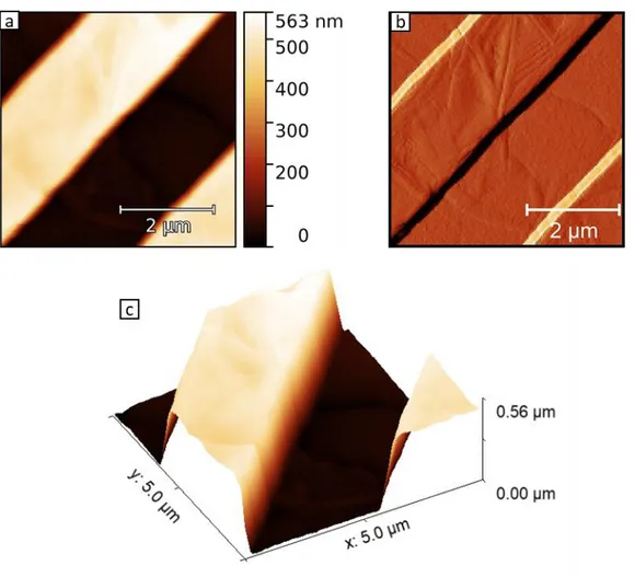
Figure 3.1: Investigation of P(VDF-TrFE) micropatterned thin film by non-contact mode force microscopy a) topography, b) NCM error signal c) three dimensional, not to scale representation of the topography.
26
microscopic measurements and are in detail described in the literature. Here I use the PFM measurements and the known 𝑑33 value to calibrate the instrument sensitivity.
The first step was to find a suitable area for the studies. Figure 3.1 shows the result of a 256pixels scan of a 5μm × 5μm area of the P(VDF-TrFE) sample surface. The choice for the tip was on an NSC36/Cr-Au, thus, line scans were performed in Non-Contact mode in order to not damage its Cr-Au coating. In Figure 3.1a we can appreciate the surface of the polymeric sample. The image provides an insight on its repetitive pattern, which goes on along the whole surface. As it is clear from the false-colour legend alongside, the darker areas correspond to wells, whereas the lighter ones correspond to peaks. Both wells and peaks are about 2μ𝑚 wide. Moreover, the height of the peaks above the wells is around 500 − 600nm. In Figure 3.1c, a three-dimensional not to scale representation of the scanned area is provided to better appreciate its morphology. In addition, Figure 3.1b shows the NCM error signal acquired during the EFM. The error signal shows more clearly the local contrast in surface topography and crystalline structures appear embedded in the amorphous phase. The few crystallites observed are long and thin with a dimension around hundreds of nanometres long and tens of nanometres thick, with directions randomly oriented.
Figure 3.2: P(VDF-TrFE) a) topography and b) three-dimensional not to scale repre-sentation of a well area.
27
Once the morphology of the sample was clear, the next step was to position the probe on a well area and perform a PFM scan. Even though wells and peaks are both piezoelectrically respon-sive, the choice for the firsts was made because of the thinness of the film. Indeed, a thinner film has also a lower coercive field, thus a polarization switching of piezoelectric domains can be achieved at lower potentials. Figure 3.2a provides an insight on a well surface morphology. The 1μ𝑚 × 1μ𝑚 scan shows that its surface has differences in height of about 50𝑛𝑚.
Figure 3.3: PFM on an unpolarized well area of the PVDF-TRFE sample. a) PFM Amplitude, b) PFM Phase response, c) Distribution of phase response, overall and domain to domain view, d) domains referred to as “lighter areas”
28
This applies for the whole sample, allowing us to state that wells are almost flat surfaces. Figure 3.2b provides a three-dimensional representation of the scanned area, in which the magnitude of the height is not to scale to better appreciate the morphology.
Once above a suitable well, a first set of PFM analysis was performed in order to reveal the piezoelectric properties of the polymer. The first step was to apply a +3𝑉AC bias to the tip and measure the PFM amplitude response of a 1μ𝑚 × 1μ𝑚 area positioned in a well of the sample. The response is plotted with a pictorial representation as explained by the legend alongside. From the image, we can see that some areas behave differently than their neighbourhoods. For instance, the lighter areas, presents larger deformations under the influence of the electric field. An explanation for this phenomenon is that among the crystal phase, some polarization vectors are coherently aligned in Weiss domains. As it is evident, the values are provided in mV, be-cause the data we acquired through the PSPD. A conversion from 𝑣𝑜𝑙𝑡𝑠 to 𝑚𝑒𝑡𝑒𝑟𝑠 can be done knowing the 𝑑33 component of the polymer and the applied bias throughout the formula:
𝑑33 [m/V] =𝐷17𝑘𝐻𝑧[𝑚]
𝑉17𝑘𝐻𝑧[𝑉] (3.1)
where 𝐷17𝑘𝐻𝑧[𝑚] is the deformation in meters of the sample reacting to 𝑉17𝑘𝐻𝑧[𝑉], namely the 17kHz bias.
As stated at the beginning of the chapter, the 𝑑33 component for P(VDF-TrFE) is assumed from
literature in order to be used for the extraction of the instrument sensitivity. The PFM phase response of the sample is provided in Figure 3.3b. As we can see, from the analysis arise two types of domains, exposed by different colours. Different areas of the well surface react in different ways to the AC bias depending on the orientation of their corresponding polarization vectors. As we can see, light areas, explicitly evidenced in Figure 3.3d, mainly present a phase response that stands around a small neighbourhood of +80°. Meanwhile, the darker areas pre-sent a distribution mostly around −90°. Indeed, they both represent native polarization do-mains, or Weiss domains. In Figure 3.3c, we can best appreciate the distribution of the phase of the domains. A large component of phase vectors is around +90°; nevertheless, we have a significant component also for the randomly oriented ones.
Once the response to the PFM investigations was detected, a polarization of the sample was performed. This latter consists in applying a bias to the tip or to the sample. If the bias is large
29
enough, an orientation and alignment of the polarization vectors of the crystals can be achieved. The procedure was performed equipping a multi75E tip. The choice of the tip was done in order to better operate in Contac Mode and thus better polarize the sample. The polarization was then performed in EFM by applying ±10VDC to the sample, while keeping the tip at ground poten-tial.
Figure 3.4 Demonstration of polarization switching in PVDF-TRFE thin film. The area scanned is different from the one of figure 3.3. Before the acquisition of the image, the whole area was polarized with a -10V bias. Then the sole left half of the shown area, was polarized with a +10V.
Figure 3.4: PFM on a polarized well area of the PVDF-TRFE sample. a) PFM Am-plitude response, b) PFM AmAm-plitude response distribution for differently polarized domains, c) PFM Phase response, b) PFM Phase response distribution for differ-ently polarized polarize.
30
A 180° change in the EFM phase signal is observed while the EFM amplitude remains of similar magnitude.
The results are shown in Figure 3.4a. The EFM amplitude response is larger in the left half than the right one. This fact is also visible in Figure 3.4b, where the distribution of the EFM ampli-tude is plotted. Furthermore, in Figure 3.4c we have the PFM phase response of the remnant polarization. As evident, after large enough biases are applied, two clearly defined regions arise. As we can see from Figure 3.4d, the left side reacts around a neighbourhood of −90°, whereas the right side reacts in a neighbourhood of +90°. This latter is strong evidence that the two sides of the sample were fully polarized in two opposite directions due to the two opposite biases applied. Moreover, from Figure 3.4d, we can also appreciate that the PFM phase response of the area is almost uniformly distributed in the -90°, +90° range. Moreover, among the two halves of the scanned area, we see a so-called domain wall. This region is evident both in Figure 3.4a, where it results darker, and in Figure 3.4c, where it results fuzzier. Referring to Figure 3.4b, we appreciate quantitively how less responsive this region is compared to its neighbour-hoods. Whereas from Figure 3.4d, we see that the phase of the domain wall is uniformly dis-tributed between −90° and +90°.
31
After the piezoelectric responses of P(VDF-TrFE) were checked, I proceeded in the determi-nation of the instrument sensitivity based on the known 𝑑33 value of P(VDF-TrFE). To do so, the AC bias was applied on a single point of a well in order to collect information about the inverse piezoelectric effect. This was the crucial stage of the experiment. A multi75E cantilever was used. Figure 3.5 shows the response for the bias values of 0, 1, 2, 3, 4, 0V. The data plot-ted in Figure 3.5b refer to a top-bottom line section of the values reporplot-ted in Figure 3.5 averaged on horizontal lines. As evident from the image, as the bias changes, also does the amplitude response. Indeed, to higher voltages correspond larger deformations because of the inverse pi-ezoelectric effect. Also here, the amplitude magnitude of these deformations is provided in 𝑚𝑉 because, as already stated, the data were collected throughout the PSPD. Furthermore, must to be noted that, because of the background noise, to a 0𝑉 bias corresponds a non-null PFM am-plitude response. The overall behaviour of the P(VDF-TrFE) perfectly accords with its already known piezoelectric proprieties.
Figure 3.5: PFM on a single well point of P(VDF-TrFE) thin film. a) PFM amplitude response, b) top-bottom horizontally averaged cross section of the PFM amplitude re-sponse.
32
Recalling Equation 2.10, an estimation of the instrument sensitivity can be written though the notation of this chapter as:
𝑆[𝑉/𝑚] = 𝐷17𝑘𝐻𝑧
𝐴𝐶 [𝑉]
𝑑33[𝑚/𝑉] × 𝑉17𝑘𝐻𝑍𝐴𝐶 [𝑉] (3.2)
where 𝐷17𝑘𝐻𝑧𝐴𝐶 [𝑉] is the deformation expressed in 𝑉𝑜𝑙𝑡𝑠 and 𝑉17𝑘𝐻𝑧𝐴𝐶 the AC bias applied to the tip.
In Figure 3.6 is plotted the average value of the tip oscillation amplitude for each value of AC bias. Here, errors refer to the standard deviation. From these data we can extrapolate an estima-tion of the sensitivity 𝑆 throughout the fit with the funcestima-tion:
𝐷17𝑘𝐻𝑧𝛼 [𝑉] = √𝑁 + (𝑑33[𝑚/𝑉] × 𝑉17𝑘𝐻𝑧𝐴𝐶 [𝑉] × 𝑆[𝑉/𝑚])2 (3.3)
In quation above, 𝐷17𝑘𝐻𝑧α [𝑉] is the tip oscillation amplitude which also takes the background noise N into account. This latter and the sensitivity 𝑆 are the fitting parameters. Here, value for the 𝑑33 is fixed to the standard value for the PVDF-TrFE, namely −38𝑝𝑚/𝑉. In conclusion, trhoughout this procedure, the value obtained fo the sensitivity was 𝑆 = 10.4 ± 0.1𝑉/μ𝑚. It
Figure 3.6: P(VDF-TrFE) thin film. Average PFM amplitude response to an AC var-ying tip bias, data points and their fit.
33
has to be said that for the sake of precision a calcoulation of the sensitivity should be done also for the NSC36/Cr-Au tip. However in this work I will not do it.
Once the sensitivity was calculated, Switching Spectroscopy was performed to demonstrate reversible polarization switching. An NSC36/Cr-Au tip was used and data were collected dur-ing two duty cycles, each of 70𝑠. The DC sample voltage went from −10𝑉 to +10𝑉, whereas to the tip was applied an AC bias of 3𝑉. Figure 3.7 shows -in both images- the typical features of the piezoelectric behaviour. In Figure 3.7a is presented the hysteresis loop of the phase re-sponse of the single point taken in account. Starting from a value of 0𝑉 bias, we appreciate that up to about 6𝑉 the phase remains stable around 90°, while above 7𝑉 it drastically drops at about −100°, symptom that the bias has reached its coercivity value. The same happens when-ever the potential reaches a value of about −7𝑉. Here the phase response reaches again +90°, symptom that a new coercivity value has been reached. The image also shows that as the exter-nal bias reverses its modulus the phase does a 180° change in its value, thus an estimation for the coercive potential of about 15𝑉 can be made. Besides, Figure 3.7b shows the characteristic “butterfly” loop of the amplitude response to the Switching Spectroscopy analysis. Here, as the bias reaches the coercivity value, the amplitude response drops to zero. An intuition to this phenomenon is that, for biases near and near the coercivity value, the amplitude gets larger and
Figure 3.7: Switching Spectroscopy on P(VDF-TrFE) thin film. a) typical hys-teresis of polarization, b) typical butterfly loop of the piezoresponse.
34
larger, but because the increasing disorder of the system, which is still not enough stimulated to orient in coherent directions, the overall resulting oscillation is minimal. These observations complete the observation on the switching behaviour of the P(VDF-TrFE).
3.2 ZnO
As the sensitivity was extracted from the P(VDF-TrFE) analysis, we were able to proceed with the measurements on ZnO. Figure 3.8a shows a 36μ𝑚 × 36μ𝑚 scan of the surface where the
ZnO crystals were deposited. A three-dimensional not to scale representation is also provided
in Figure 3.8b. These images were the starting point for the determination of the structures to analyse. All investigations were done implementing a 𝑚𝑢𝑙𝑡𝑖75𝐸 tip in Non-Contact in order to avoid crystals shifting and damage from the tip dragging. Figure 3.8c shows the selected
Figure 3.8: investigations of 𝑍𝑛𝑂 by non-contact mode force microscopy. a, b)
To-pography and not to scale three-dimensional representation of the sample surface; c, d) topography and not to scale three-dimensional representation of a ZnO crystal.
35
structure for the following PFM investigations. As evident from the three-dimensional not to scale representation in Figure 3.8d, the structure appears solid with sharped and nicely defined edges. This leads us to speculate it being an actual well grown crystal.
Once the crystal was selected, the probe was landed on a single point of its surface in order to proceed with the PFM investigation. As was done for the P(VDF-TrFE), an AC bias was ap-plied to the tip for the values 0, 1, 2, 3, 4, 0V. Each pixel of Figure 3.9a) represents a data point which together encapsulate the results of this procedure. The response of the sample sur-face to stimuli is plotted in Figure 3.9b. Here is presented a bottom-top cross-section of the values reported in Figure 3.9a averaged on horizontal lines. As for the P(VDF-TrFE), an in-creasing bias leads to an inin-creasing PFM amplitude response. This is a strong evidence of the piezoelectric proprieties of the ZnO crystal. Also here, must to be noted the non-null value of the PFM amplitude for a null bias applied. This again, founds its roots in the background noise registered by the tip.
Figure 3.9: a) PFM Amplitude response to a varying bias of a single point of the ZnO crystal, b) bottom-top horizontally averaged PFM Amplitude re-sponse.
36
Starting from the response of the crystal to the external electric field, it was possible to extract the value of its 𝑑33 component. Figure 3.10 shows, as was done for the P(VDF-TrFE), the mean
value of the tip oscillation for each AC bias to the tip, with errors referring to the standard deviation. From this the 𝑑33 value is computed throughout Function 3.3, using this time 𝑑33 as a fitting parameter and keeping the sensitivity 𝑆 as the one obtained from the P(VDF-TrFE) analysis. Throughout this procedure, the value we obtained was 𝑑33= 10.36 ± 0.03𝑝𝑚/𝑉.
This value results a bit larger than the literature one of 15 ± 2 𝑝𝑚/𝑉, but still in the same order of magnitude. This concludes our investigations on 𝑍𝑛𝑂.
Figure 3.10: PFM response of a ZnO nanocrystal. Average PFM amplitude re-sponse to an AC varying tip bias, data points and their fit.
37
3.3 ZnSnO
3Once the value of the 𝑑33 of the 𝑍𝑛𝑂 was computed, the next step of our analysis was the one
of the ZTO. Figure 3.11 shows a 10μ𝑚 × 10μ𝑚 scan of the surface where the ZTO structures were deposited. A three-dimensional representation is also provided in 3.8b. As for the 𝑍𝑛𝑂, the choice for the tip was made in order to perform in Non-Contact mode and avoid damages of the sample. On this turn the choice was on a 𝑁𝑆𝐶36/𝐶𝑟 − 𝐴𝑢 𝐼. From the scanned area, the structure exposed in Figure 3.11c was chosen for the following PFM analysis. As evident from the three-dimensional representation offered in Figure 3.11d, the structure occupies an almost cubic volume with a side of about 500 − 600𝑛𝑚. Nevertheless, from a visive analysis its edges do not result sharp as were the ones of ZnO. Furthermore, its surface presents huge inequalities.
Figure 3.11: investigations of ZnSnO3 by non-contact mode force microscopy. a, b)
Topography and not to scale three-dimensional representation of the sample sur-face; c, d) topography and not to scale three-dimensional representation of a ZnSnO3
38
These observations led us to speculate the structure being an agglomerate of smaller sub-struc-tures rather than a well-defined solid crystal.
Once the suitable structure was selected, the probe was landed on a single point of the surface in order to proceed with the PFM investigation. As was done for P(VDF-TrFE) and ZnO, an AC bias of 0, 1, 2, 3, 4, 0V was applied to the tip. Each pixel of Figure 3.12 codifies the results of this procedure. The response of the sample surface to the stimuli is plotted in figure 3.12b as the top-bottom cross-section of the values reported in Figure 3.9a averaged on hori-zontal lines. As for the previous samples, an increasing bias leads to an increasing PFM ampli-tude response. As before, this is an evidence of the piezoelectric behaviour of the structure. Also in this case, because of the background noise, to a non-null bias does not correspond a null amplitude.
Starting from the response of the structure to the external electric field, it was possible to extract the value of its 𝑑33 component. Figure 3.13 shows, as was done for the P(VDF-TrFE) and the
ZnO, the mean value of the tip oscillation for each AC bias to the tip, with errors referring to
Figure 3.12: a) PFM Amplitude response to a varying bias of a single point of the ZTO crystal, b) top-bottom horizontally averaged cross section of the PFM Amplitude re-sponse.
39
the standard deviation. From this, the 𝑑33 value is computed throughout Function 3.3, using
this time 𝑑33 as a fitting parameter and keeping the sensitivity 𝑆 as the one obtained from the
P(VDF-TrFE) analysis. Throughout this procedure, the value we obtained was
𝑑33= 23.70 ± 0.04𝑝𝑚/𝑉.
Figure 3.14 then shows the comparison between the data of the ZnO and 𝑍𝑛𝑆𝑛𝑂3 structure. As
evident, the latter material is more responsive than the former.
Figure 3.13: ZTO crystal. Average PFM amplitude response to an AC varying tip bias, data points and their fit.
Figure 3.13: ZTO crystal. Average PFM amplitude response to an AC varying tip bias, data points and their fit.