1
UNIVERSITY of ROME
"TOR VERGATA"
Department of Chemical Science and Technology
XVII Ph.D. Course on “Materials for Environment and the Energy”
Thesis of Doctorate
POROUS SILICON MATERIALS DEVELOPMENT FOR
APPLICATIONS IN ENVIRONMENTAL SENSORS
Dr. Veronica Valentini
Internal tutor External tutor (CNR)
Prof. Riccardo POLINI Dr. Giorgio MATTEI
2
CONTENTS
INTRODUCTION...4
CHAPTER 1 ...7
POROUS SILICON PROPERTIES...7
1.1 PREPARATION: Electrochemical Reactions and Formation Processes...9
1.2 DISSOLUTION CHEMISTRIES ...13
1.3 RELATIONS BETWEEN PREPARATION AND PROPERTIES OF THE PS LAYERS...13
1.3.1 Properties dependence from the used Si type ...15
1.3.2 Effect of Illumination...16
1.3.3 Effect of the solution composition...17
1.3.4 Current density effects ...18
1.3.5 Anodisation time effects ...18
1.4 Post treatment and oxidation, functionalization...18
1.4.1 Drying ...19 1.4.2 Storage of PS...19 1.4.3 Controlled Oxidation ...21 1.4.4 Capping ...21 1.4.5 Functionalizations ...22 1.5 Applications ...22
1.5.1 Applications in optoelectronics (PL and EL)...23
1.5.2 Optic and Spectroscopic Applications of PS multilayer systems ...24
1.5.3 Sensors and functionalization ...28
1.5.4 Solar cells...29 CHAPTER 2 ...30 EXPERIMENTAL PART...30 2.1 Samples preparation ...30 2.2 Samples post-treatments ...32 2.2.1 Oxidation...32 2.2.2 Functionalization...33 2.3 Samples characterization...34 2.3.1 Gravimetric Analysis ...34 2.3.2 SEM analysis ...34
2.3.3 Raman spectroscopy analysis ...35
2.3.4 Fourier Transform Infrared Spectroscopy (FTIR) analysis ...35
CHAPTER 3 ...37
RESEARCH ACTIVITY...37
PARTI:EFFECT OF THE INTERACTION OF PS WITH THE ENVIRONMENT...37
3.1 Study of the induced oxidation in air of ps in presence of pyridine vapor ...37
3.2 Study of the induced oxidation in air of ps in presence of different organic base vapors...43
3.3 Study of the interaction between ps and urotropin vapor: possible dosimeter ...49
3.4 Sum frequency generation spectroscopy of ps layers ...53
PARTII:FUNCTIONALIZATION OF PS LAYERS IN VIEW OF APPLICATION AS ENVIRONMENTAL AND BIOLOGICAL SENSOR...61
3
3.5 Systems realizzation for sensoristic applications ...61
STANDARD FUNCTIONALIZATION PROCEDURES...61
3.5.1 Electrochemical Reaction ...61
3.5.2 Photochemical Reaction...62
3.5.3 Thermal Reaction...63
3.5.4 Chemical Reaction ...63
3.6 a New functionalization method...63
3.6.1 The Method...63
3.6.2 Functionalizzation by Contact in the etching solution...68
3.6.3 Comparison of the functionalization by contact in the etching solution of oxidized and fresh PS samples...69
3.6.4 Ageing Study ...70
3.6.5 Spatially Confined PS Functionalization ...72
3.6.6 Other Organic Molecules...77
3.7 Two steps functionalization of PS samples ...80
CONCLUSIONS ...87
Interaction of PS with the environment ...87
PS Functionalization ...88
REFERENCES...91
ANNEXES...97
A.CRYSTALLINE SI: GENERAL INFORMATION AND PROPERTIES...97
B.RAMAN SPECTROSCOPY...105
C.FOURIER TRANSFORM INFRARED SPECTROSCOPY AND INSTRUMENTAL CORRECTION IN THE CASE OF REFLECTANCE SPECTROSCOPY...110
D.SCOUT ELABORATION AND BRUGGEMAN MODEL...115
E.SFGSPECTROSCOPY: GENERAL INFORMATIONS AND PROPERTIES...118
1. Non linear optics Theory ...118
2. SFG Intensity Calculation...121
3. Direction of the reflected SFG wave...125
4. Intensity of the field electric SFG ...127
4
INTRODUCTION
In these last years we have seen the consolidation of a diffused interest in the environmental monitoring problems in its amplest meanings. The smog pollution problem, and in general, of the environmental impact consequential from all the activities developed in the urban centers, has been faced in a systematic way since the first '70s, using special tools both legislative and technological. According to the most recent indications of the EU the attention is concentrated on thematic of remarkable social-economic interest, and particularly on the following action areas: environment, health, innovation in product and process, microsystems and nanotechnologies.
Among the materials used in the environmental sensors porous silicon, PS, can also be enumerated. PS is the product of the partial anodic dissolution of a substrate of crystalline silicon in an electrolytic solution of hydrofluoric acid, HF. PS is a material of wide importance not only for fundamental studies, for example for quantum confinement studies and for the chemistry of the surfaces, but also in application for its properties of photoluminescence and electroluminescence in the visible, its large superficial area and its optical properties [1]. All these characteristics have greatly increased researchers’ interest in PS, opening a very active research area in constant expansion, especially for applications in the fields of the opt-electronics, optics and sensors. With the use of PS, among of the applications, light emitters, solar cells, interferential filters and sensors devices have been made; other applicative purposes of PS production and industrial use of PS as a sacrificial insulating layer in electronic devices and as electrode in fuel cell are well known.
PS is a material of wide interest in the sensors field because of its large surface area, surface reactivity and natural integrability in the electronic circuits. Therefore, the study of the interaction between the environment, namely liquid phase and/or gas phase, and the PS surface is of great importance in applications. PS, can be used as transducer material in sensing application, and in particular in the detection of vapors, liquids and biochemical molecules. In fact, when exposed at chemical substances, several physical quantities, such as refractive index, photoluminescence, and electrical conductivity, can change drastically. Moreover, PS is an available, low cost material, with a large surface area that can assure a very effective interaction with several adsorbates, so that it could usefully be employed in the realization of sensors and microsystems.
5
For all these reasons we have prepared single layers and specially devised PS superstructures and studied in details some aspects of the interaction between the PS materials with the environment that is a crucial point for application in the sensor field. The first subject of our research has been the oxidation process of PS in air and its control. In fact, we know that in presence of air, or water and/or oxygen, PS inevitably gets oxidized so modifying its properties and the performances of its devices. But a controlled oxidation of PS materials can be also used as method to stabilize the properties of this material. Indeed oxidized PS can be used for different application, for example a laser light stimulated emission from nano-structured silicon in a silicon oxide matrix has been recently demonstrated [2]. Besides, applications of oxidized PS in the environmental sensor field have been reported [3 ÷ 7].
On the basis of these interests, a thorough study of PS oxidizing phenomena in different environments, namely air alone or saturated with vapors of some organic substances (in recent work the Pyridine has been suggested as a catalyst for PS oxidation in air [8]), has been performed.
During this research doctorate course we have verified that the use of PS multilayer optical systems, e. g. Fabry-Perot, FP, increases the response sensibility of the system (due to the optical signal amplification that occurs inside the structure) and thus of the sensibility of the possible optical sensors. Therefore we have applied one of our FP structure to realize a dosimeter for the urotropin, toxic organic substance commonly used in several application areas, e.g. rubber, explosives, fuel, pharmaceutical industries, etc.. Following the tendency of recent literature we start to work on the functionalization of PS with the aim of use organic molecules having peculiar properties “ad hoc” for sensor applications. Functionalize a PS sample means to substitute the Si-H bonds normally presents on the whole surface of fresh PS with Si-C covalent bonds that therefore bond in a stable manner a certain organic molecule to the PS surface (e. g. chemisorptions by hydrosilylation reaction). The coverage of the PS surface with suitable organic molecule can attribute new properties to the PS, those owning to the organic molecule and others deriving from the organic-PS match, but it can also stabilize the sample and reducing the effect of the oxidation due to the aging of the PS. In the PS functionalization activity we have, finally, invented a new PS functionalization method simple, fast and effective and that present the unique ability to allow the confined functionalization of a selected layer in a PS stack. We have developed this study with the aim to exploit at the best its potentialities, also as first step to realize sensors of novel design.
PS produced samples have been characterized by SEM and optical spectroscopies, FTIR, UV-Vis, Raman and sum frequency generation (SFG), which are particularly suitable for thin layers
6
and surfaces studies. After the post-treatments, the species present on the PS surface, resulting from the functionalization, have been determined using the FTIR reflection spectroscopy and, in the case of the study of oxidation, the evolution of the various species on time has been followed.
Finally, the presentation of the subjects of this thesis is the following:
• In chapter 1 after a short historical introduction general information regarding the PS main properties and the possible applications are presented;
• In chapter 2 is presented the experimental part that include information on the sample preparation and characterization;
• In chapter 3 are presented in detail and discussed the results of the research activity: the study of the PS induced oxidation in humid air saturated by HB2BO, Pyridine and other organic base vapors; the study of the interaction between PS and saturated vapors of Urotropin (with the demonstration that our samples can be used as a dosimeter for this toxic substance used in several application areas, e.g. rubber, explosives, fuel, pharmaceutical industries, etc.); the first measurements of PS surface species using a non linear spectroscopy highly sensitive to the surface i.e. SFG spectroscopy; the results obtained on the functionalization of PS layers that include the description of a new original method of in-situ formation-functionalization PS;
• finally there is the summary.
At the end there are several annexes: some general information and properties about the crystalline Si (annex A); some indication about the theory of Raman (annex B) and Infrared (annex C) spectroscopies; an illustration of the SCOUT elaboration and of the used Bruggeman model (annex D); short notes describing general information about the SFG spectroscopy (annex E).
Finally a list of all the publications regarding the scientific research activity carried out during the last three years.
7
CHAPTER 1
Porous Silicon properties
PS which forms on the surface of crystalline Si substrate in hydrofluoric acid (HF), under an appropriate anodic polarization, was first observed by Uhlir in 1956 [9]. He investigated electropolishing of crystalline Si and found that below a certain current density a brownish layer develops, which is now known as PS. Later on, PS was investigated in detail by Turner (1958) [10]. As the name PS indicates, the bulk crystalline Si changes by the etching process into a kind of sponge-like structure with interconnected and hydrogen covered silicon columns and pores, as shown in Fig. 1.1.
Fig.1.1. Scheme of PS layer structure (1) overhanging the crystalline Si substrate (2).
Uhlir had already noticed that flakes of PS appeared sometimes of red color (indicative of an increase of the “band gap” in comparison to the Si crystalline of the “bulk”), in 1984, Pickering et all. [11] had reported for PS the measure of photoluminescence (PL) in the visible at 4 K. In 1990 Canham [12] found strong visible room temperature (RT) photoluminescence in a PS layer which had been etched chemically in HF after the anodic etching in order to widen the pores and therefore decrease the size of the remaining Si skeleton.
The observed luminescence was much more efficient, than the usual band gap related IR luminescence of crystalline bulk Si (which has an indirect gap of 1.1 eV) as showed in Fig. 1.2.
8
Fig. 1.2. Comparison between photoluminescence spectra at room temperature of the crystalline Si substrate and the PS. The photoluminescence intensity expressed in a logarithmic scale.
The observation of efficient room temperature (RT) photoluminescence in the visible range combined with the quantum confinement explanation attracted a large interest, both fundamental and applicative, on PS.
The main PS properties are:
1. Strong PL (and EL) in the visible: interesting for optoelectronic applications; 2. Large surface area (up to 900 mP
2
P
/g): interesting in chemical and biochemical sensing;
3. Dielectric function (ε) that can be easily modulated. Indeed by varying the porosity, defined as the vacuum volume fraction, it is possible to obtain several values of the dielectric function, which is basically the sum of contributions from the skeletal crystalline Si and the air on the pores.
4. It is also possible to produce multilayer systems with various porosity changing the applied current density during the anodization because the porosity depends on the current density and the thickness on the anodization time. One of these multilayer systems is the Fabry-Perot (FP) that is a structure of PS at high reflectivity (100%), with a cavity, a reflectivity minimum, in the center of this high reflectivity region. This property makes the PS interesting for optical, spectroscopic and sensing applications.
5. PS is also a biodegradable and biocompatible material, property interesting for medical and biological application.
6. Easy integrability in the Si microelectronics.
General information, also about possible applications, are reported in numerous reviews and articles devoted to the PS [1, 13 ÷ 17].
9
1.1 PREPARATION: Electrochemical Reactions and Formation Processes
The partial anodic dissolution of crystalline Si samples occurs under suitable conditions in electrochemical teflon cells containing an HF electrolytic solution.
In Fig. 1.3 are shown some typical electrochemical cells in use. In this work the typology of cell used was the (c) one that is simple and allows to realize homogeneous samples presenting a good control of the porosity and thickness.
Fig. 1.3. Schemes of anodization cells used for the electrochemical PS formation reaction: (a) cross section of a double tank cell; (b) cross section of a lateral anodization cell; (c) cross section of a conventional single tank cell.
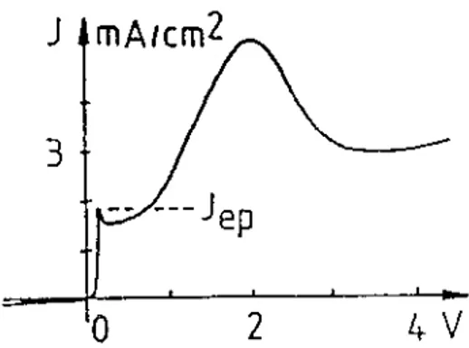
Observing a typical current density (J)/electrodic potential (V) curve, Fig. 1.4, for J > JBepB the electropolishing occurs and for J ≤ JBepB the PS formation occurs.
(b) (a)
10
Fig. 1.4. Dependence of the current density on the potential in a Si sample submitted to the anodization.
The JBepB depends mostly on the composition of the HF solution in EtOH and little on the substrate. A large variety of layers morphologies (pore diameter, pore spacing, direction of propagation, etc.) may be obtained with single crystalline Si, according to the substrate (surface orientation, doping level and type) as well as the composition of the aqueous solutions (pH, HF concentration, etc.) and to the anodization conditions (J and t).
The skeleton remaining among the channels preserves its original crystallinity, showing that pore formation occurs through a direct dissolution of the bulk of the material and not by some redeposition or recrystallization process.
The exact Si dissolution chemistry is still matter of discussions, although it is generally accepted that the holes are necessary in the initial oxidation stage both for the electropolishing and for the pore formation. In-situ and ex-situ spectroscopy has confirmed the presence of Si-H bonds in the surface during the PS formation. The hydrogen exists on the Si surface in at least two different forms, Si-H and Si-HB2B, with a third possible form Si-HB3B (the superficial concentration of the dihydride, Si-HB2B, increases with the increase of the anodic potential).
The (100) plane has the more sterically favorite geometry for the Si divalent superficial state, that is two bonds symmetrically direct inside the solution, important preferential site of the anodic etching.
The presentation and discussion of the various proposed models, in literature, for the PS electrochemical formation processes in the HF various solutions, go beyond the purposes of the present treatment. Therefore, the interested reader can consult the specific articles quoted in the bibliography and associated to the various models indicated in the following list:
1. The “Beale” model [18, 19];
2. The “diffusion-limited” model [18, 20]; 3. The “quantum-based” model [18, 21]; 4. The “Zhang” model [19];
11
6. Mathematical models with growing simulations [22 ÷ 24].
We present here a general scheme of p-type Si dissolution process, in HF ethanoic solution, the aim is to emphasize the two fundamental steps of the process (universally accepted): (i) The Si dissolution that involves hole (hP
+
P
) participation, at the interface Si/electrolyte and (ii) the passivation, namely the end of this process, when the hole supply is interrupted, and that causes the stability of the produced PS structure.
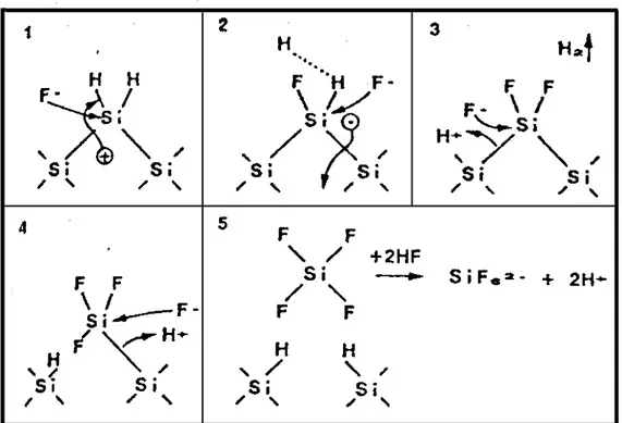
Before to start the anodic dissolution the Si thin plate is kept in contact for few minutes with the HF solution to eliminate the native oxide (SiOB2B) always and inevitably present on the crystalline Si surface leaving it H-terminated [10]. Indeed, although the bond energy for the Si—F bonds is the highest of all superficial species (see table 1.1), such bonds, thermodynamically more stables, are not observable on the Si surface, because they hydrolyze easily to Si —OH and Si — H in presence of water. The SiH species present on the Si surface depends on the Si substrate orientation; PS layers produced from a (100) Si plate, as in our case, present their surface mostly SiHB2B-terminated.
Table 1.1. Bond energies for various bond type presents on the crystalline Si surface. Bond type Bond energy (Kcal/mol)
Si—F 129.3 Si—O 88.2 Si—H 70.4 Si—Si 42.2
In some detail the formation process of PS during the anodization procedure can be summarized as it follows:
When a hole (hP
+
P
) reaches the Si hydrogenated surface fluoride ions nucleophilic attack can occurs on Si—H bonds and a Si—F bond is established (step 1 Fig. 1.5).
12
Fig. 1.5. Porous Si formation reaction scheme starting from a crystalline Si substrate in an HF ethanoic solution by anodic dissolution reaction.
Due to the polarizing influence of the first fluorine Si-bonded atom, another FP
-P
ion can attack the other Si-H bond of the same Si atom under generation of an HB2B molecule and injection of one electron into the electrode (step 2). Due to the polarization induced by the Si—F groups, the electron density of the Si—Si back bonds is lowered and these weakened bonds will now be attacked by HF or HB2BO (step 4 and 5) in such a way that the Si surface atoms remain bonded to hydrogen (step 5). The dissolved Si will remain in solution as species HB2BSiFB6B that appear in some ionized forms according to the concentration and pH of the HF solution.
If a Si atom is removed from an atomically flat surface by this reaction, an atomic size dip remains. This modification in surface geometry will change the electric field distribution in such a way that hole (hP
+
P
) transfer occurs at this location preferentially. The defect points on the Si surface generates a local concentration of the electric field that increases the hole concentration in these regions that becomes larger than in the other Si surface regions passivated by Si-H bonds.
At a certain point the dissolution reaction breaks off. This self-limiting process, that gives rise to the Si surface passivation and to the stabilization of the produced PS structure, can be attributed to different mechanisms: (i) if the pore walls are lacking in holes they will be protected against further dissolution. While the Si skeleton size decreases the supply of free carriers diminishes (hole depletion) and its resistivity increases until reach the intrinsic Si
13
value [1 (g), 25]. (ii) The thinning of the Si skeleton can reduce and stop the dissolution reaction, because of the quantum confinement of the charge carriers due to the small pore wall dimensions. This quantum confinement provokes a gap widening and an energy barrier DEBVB for holes and DEBCB for electrons formation to come into the Si region between the etched pores [21].
Similar processes occur for the n-type Si samples, in this case, because they have an excess of electrons, the necessary holes for the anodic dissolution process are produced exposing the samples to a controlled lighting. In the dark n-type Si samples anodization occurs only at high potential and the resulting structure is different from that obtained at same operative conditions but under illumination.
1.2 DISSOLUTION CHEMISTRIES
When Si samples remain in contact with the HF solution for long times, a dissolution of purely chemical nature is added to the phenomenon of the electrochemical dissolution. The contribution of the chemical dissolution has therefore a larger impact in the layers formation of thicker PS, in fact, for p-type Si samples, increasing the layer thickness of a factor 5 the average porosity increases of 10% and the peak of the pore size distribution increases of 3 nm [1 (a)].
For the substrates heavily doped (e. g. ρ = 0.01 Ωcm) the effect of the chemical dissolution on the porosity is negligible and not measurable due to the low specific surface area (200 mP
2 P cmP -3 P ) of the material, compared to that of the layers obtained from low resistivity Si (~600 mP
2 P cmP -3 P ). In the case of n-type porous layers, the pore radii increase and the distribution broadens when the sample thickness is increased, because the contribution of the chemical dissolution is added to the electrochemical one.
1.3 RELATIONS BETWEEN PREPARATION AND PROPERTIES OF
THE PS LAYERS
In this paragraph the relations are described between the parameters preparations (for example the type of substrate, the composition of the electrolytic solution, etc.) and the characteristics of the PS produced layers (porosity, morphology, pore dimensions, etc.).
All the properties of the PS layer, such as porosity, thickness, pore diameter, microstructure, are strongly dependent on the anodization conditions. These conditions include the HF concentration, the pH of the solution and its chemical composition, current density, wafer type
14
and resistivity, crystallographic orientation, temperature, anodization duration, stirring conditions and illumination conditions during anodization. Optimum control of the porous layers fabrication and the reproducibility are possible only if all the parameters listed above are taken into account.
In the most general sense a “pore” is an etch pit whose depth, d, exceeds its width, w. Generally single pores are generally closed at one end and partially interconnected to some degree. The most common shape by far is that of cylindrical pores with varying degrees of “branching” and “necking”. The use of chemically aggressive electrolytes, excessively long anodization times or light-assisted etching all act to generate a funnel-type shape. The anodization of (100) oriented wafers can generate pores of square cross-section whilst (111) oriented wafers can exhibit triangular shaped pores [1 (b)].
The IUPAC defines pore size ranges, reported in the table 1.2, where are associated different PS typologies:
Table 1.2. Definition of the pore typology as a function of the width range.
Pore width (nm) Pore type
§ 2 Micro
2π50 Meso
> 50 Macro
Clearly, pore size only has a precise meaning when the geometrical shape of the pores is well defined and known. For low porosity macroporous Si, and sometimes of mesoporous Si, this is the case, but micro pore shape is currently ill-defined. Extreme caution, however, is needed to distinguishing rough surface from incipient pore formation via surface topography measurements relying on “Atomic Force Microscopy” (AFM) or “Scanning Tunneling Microscopy” (STM) alone. Such images can be significantly distorted in the vertical direction and completely miss or underestimate the depth of very narrow features. Individual pore examination is most frequently made by high resolution transmission electron microscopy (HRTEM) or high resolution scanning electron microscopy (HRSEM).
Pore size determines much of the absorptive properties of a material, and that are important in application area such as sensing or biofiltration.
15
U
1.3.1 Properties dependence from the used Si type
The pore nucleation starts from the defect sites on the crystal surface, therefore the doping atoms are selectively removed during the anodization process leaving an intrinsically porous structure. This allows to explain the dependence of the pore density on the doping level. A gradual increase of the pore number and the decrement of their radius to the increasing of the semiconductor doping level occur. The pore size increases with the decrease of the resistivity for the p-types and vice versa for the n-types (that is the size increases with the increasing of the resistivity) [19].
Increasing the doping concentration also the pore diameter and the average skeleton dimensions slightly increase (the pP
+
P
-type produce formation of channels) [18].
The characteristic curves J/V for p-type Si wafers of different dopant concentrations in an HF solution are independent of the thickness of the PS layer and successive potential sweeps on the same Si electrode lead to the same dependence [1 (c)]. When the doping concentration increases the curves shift towards cathodic potential, as we can observe in Fig. 1.6 [1 (c)]. As a consequence, of this if a Si wafer with an average dopant concentration is anodized the PS formation takes place previously in the heavily doped regions producing a spatial selectivity.
Fig. 1.6. Anodic current density-voltage characteristics of p-type Si in a 35% HF solution and with e of different substrate doping concentrations.
16
The relation J/V depends also on the relative doping of the material: the curves J-V for every type of samples are moved to the right in the general order nP
+ P < pP + P < p < n, see Fig. 1.7 [1 (c)]. If the potential is controlled with care to the appropriate value, the pore formation occurs in preferential way for the different types of dopants: nP
+
P
can be preferentially anodized over pP
+ P , p or n; pP + P
can be preferentially anodized over p or n; etc…
Fig. 1.7. Comparison of the anodic current density-voltage characteristics obtained from p- and n-type Si in a 35% HF solution using substrates of different doping levels (nP
+ P and pP + P : 10P 19 P cmP -3 P , nP -P and pP -P : 10P 15 P cmP -3 P ). U 1.3.2 Effect of Illumination
Si dissolution requires holes (hP
+
P
). When lightly doped n-type Si (~10P
18 P cmP -3 P ) is anodized in the dark, PS formation is observed only at high voltages (>5V) and macroporous layers are obtained (pore diameter ~0.2 µm). If the anodization is performed under illumination, PS is formed at lower potentials (< 1V) and the resulting material consists of two parts: the top surface layer is nanoporous (d ~3 nm) and its thickness lies in the 0.2 ÷ 1 µm range, depending on the doping of the substrate. The underlying part is macroporous. For a heavily doped substrates (~10P
19 P cmP -3 P ) PS formation is observed even in the dark [1 (c)].
The anodic dissolution of p-type Si generally is performed to the dark because the p-type generally is not very sensitive to the presence to the lighting.
17
U
1.3.3 Effect of the solution composition
When for the PS formation a purely aqueous HF solution is used, the hydrogen bubbles stick to the surface inducing lateral and in-depth inhomogeneity. To improve the uniformity of the PS layer these bubbles must be quickly eliminated and one of the most appropriate means to overcome this problem is to add surfactant agents to the HF solution.
The more used surfactant in the case of the PS formation is absolute ethanol and it is known that for an efficient elimination of the bubbles the ethanol concentration should not be less than 15% [1 (c)]. It has been shown [26, 27] that the ethanoic HF solution completely infiltrates the pores, while a purely aqueous solution does not, due to wettability and capillary phenomena (the Si surface hydrogen terminated is hydrophobic [26, 27]).
These phenomena play an important role in the smoothness of the interface between Si and PS and thus in the uniformity of the PS thickness. In fact, the role of the ethanol is to improve the uniformity of the PS layer by elimination of the hydrogen bubbles and to improve the penetration of the electrolyte in the pores.
When the electrolytic HF concentration is decreased: the radii corresponding to the maximum distribution shift to higher values, and the distributions broaden [1 (a)]. Increasing the HF concentration in the electrolyte solution decreases the PS layer porosity [1 (c)]. Lower porosity can be obtained using a higher HF concentration, at the most a solution of pure HF (50%). Nevertheless the PS layers obtained in such a solutions, without ethanol, exhibit poor homogeneity and the best way to obtain lower porosity with good homogeneity is to use acetic acid as surfactant [1 (c)].
Although commonly the most used method for the PS formation is the anodization at constant current density, in some cases (thick layers, > 50 µm, obtained at high current density, > 100 mA cmP
-2
P
) to reduce the effects of the local concentration inhomogeneity of the electrolytic solution in the PS, a pulsed current is used. Indeed during the pauses of the anodic current there is regeneration of the active species (HF) and the out-diffusion of the inactive species through the pore network. Such current regime contributes to maintain an almost constant HF concentration in the pore tips and leads to a more in-depth homogeneous layer [1 (c)].
18
U
1.3.4 Current density effects
In general at low current density the pore are randomly direct and filamentous. At current density close to the electropolishing regime, the pores assume a pipe shape [18]. Porosity increases with the increase of the current density.
For given anodization conditions (current density and HF concentration) the porosity is much higher for the thicker layer (we remember that the thickest layer is more porous due to the extra chemical dissolution of the PS layer in HF).
For p-type substrates, when the forming current density is increased, the porosity increases, and the radii of the maximum of the distribution widen, while the distribution also broaden.
U
1.3.5 Anodization time effects
The layer thickness linearly increases with the increase of the anodization time, therefore it is useful to know the anodic etching rate for the specific Si substrate. Thönissen et al [1, 28] have planed a model from which they have obtained an expression for the anodic etching rate as a function of the formation parameters, that is in good agreement with the experimentally results. The anodic etching rate r, defined as the PS volume obtained in the unity of time, is correlated to the porosity P (j), which is function of the current density, j, through the equation:
r = [j/ (P (j) n (j))][A
BrB/ [e N
BABr]
where n (j) it is the number of exchanged charge carriers per dissolved silicon atom (valence that for PS = 2) also it function of the current density, ρ the Si density (2.33 g/cmP
3
P
), ABrB the Si relative atomic mass (28.08 g/mol), e is the charge of the electron, NBAB the moles number [1, 28].
1.4 POST TREATMENT AND OXIDATION, FUNCTIONALIZATION
Some post-treatments of PS samples are shortly described, that are important for the stabilization and for successive modifications (also in sight of possible applications) of the properties of the materials, i.e.: drying, storage, controlled oxidation, capping and functionalizations.
19
U
1.4.1 Drying
After the formation of a PS samples and rinsing in some liquids (water, ethanol, pentane, etc.), during the drying the cracking of the layer can occurs, the drying, in fact, is particularly critic, especially for microporous samples.
The origin of the cracking is due to the large capillary stresses associated with the nanometric size of the pores. Based on the PS mechanical properties and on the X rays diffraction data can be seen that the cracking occurs for PS layers thicker than a critical thickness hBcB which mainly depends both on the porosity of the layer and on the surface tension of the drying liquid. The use of highly porous Si films has been limited from the mechanical fragility provoked during the drying. So among the techniques of drying, that have recently been set, trying to decrease or suppress the capillary stresses we can list the supercritical drying [1 (d), 29 ÷ 31], the freeze drying [1 (d), 32, 33], the drying with pentane [1 (d), 34] and the drying by slow evaporation rate [1 (d), 35].
U
1.4.2 Storage of PS
The morphology of PS is such that as-prepared layers can have extremely large internal surface areas (up to 900 mP
2
P
/g) and are largely passivated through relatively weak Si—H bonds. A consequence of this is that as-anodized material is unstable and chemically very reactive to the surrounding ambient. Indeed such layers readily oxidize if stored in air. The extension of the oxidation depends on the ambient humidity, temperature and storing time. The concentration of F and H atoms decrease, and impurity elements (such as C, B, S and N) gradually accumulate inside the resulting native oxide. The oxidation extent and the atmospheric contamination depends on both storage time and temperature, and is influenced by other factors such a spore morphology (macro-, micro-, or meso-porous) and storage conditions (light or dark ambient, type of container). Changes in material properties, such as electrical resistivity, strain, and optical properties, such as refractive index and photoluminescence, can accompany the ageing process.
The ageing of the PS results from the reaction of the material with the surrounding including its container.
In the most of the cases the PS is stored in air at RT. The exposure in air, however, changes gradually the structural and physical properties of the material, due to the oxidation of its inner surface. To minimize the variability and the extension of such storage effects various treatments have been suggested and applied:
20
• Intentionally oxidize the material in a controlled fashion [1 (e), (h)];
• isolate the inner surface by capping film or by storage in inert gases such as nitrogen or helium, or, finally by storage in UHV (<10P
-9
P
torr) [1 (e), (f)]; • modify its surface [1 (e), (f)];
• Impregnate the pores by suitable non-aqueous liquids such as ether or alcohols [1 (e), (f), (i)];
• Try to optimize storage time and conditions for the given application requirements [1 (e), (f)].
The storage and characterization in inert gas as NB2B or He clearly show a lower growth of native oxide, but a complete suppression is unlikely for periods of storage of weeks, unless the humidity levels and OB2B are lowered below the level of the ppm. Similar considerations are valid for storages in not aqueous liquid like ether or alcohols. Even with the drying of the electrolyte by distillation under vacuum and the degassing, the residual water to levels of ppm can produce islands of oxide that after a week cover the 60% of the surface [1 (e), 36].
For short-term uses (times or few days) the storage in ultra-pure alcohol or HF gives relatively cleaned returns of free-oxide material [1 (e), 37 ÷ 39]. Nevertheless the used concentration (HF aqueous solution 1 ÷ 10%) can increase the layer porosity of a significant amount (variation of the porosity a day < 2%) [1 (e), 40]. The PS has shown a rapid adsorption of carbon and oxygen also under vacuum of ~10P
-6
P
Torr. This contamination is minimized in UHV (< 10P
-9
P
Torr). The storage under vacuum does appreciably slow the ageing process down but it does not eliminate it, the material still pick up C and O, mainly through the variety of residual species (hydrocarbons, water vapor) that can be present within a vacuum system.
The storage into the dark is generally recommended to minimize photochemical effects. These can occur not only at the air but also during the storage in liquids as alcohol and HF. Ultra-dry inert gases or UHV storage are necessary to minimize the oxidation at RT of fresh etched material.
Both not anodized Si wafers and the anodized ones commonly are stored in plastic containers, which, while they offer protection from the contaminants of the air, such containers are able to spread some contaminants for degassing of the same container material. Due to such pollution highly porous materials can become doped with the volatile constituents of the container in which it is stored. A non luminescent material could gradually become impregnated of chromophores for example (this has been verified by accelerated ageing studies [41]) [1 (e)].
21
U
1.4.3 Controlled Oxidation
PS controlled oxidation would seem to be a simple process to realize and to control by thermal way. Due to the porosity of the material and the easy penetration of the gaseous OB2B in the pore we would expect a fast oxidation with the formation of a superficial oxide layer. Nevertheless due to the mechanical fragility solicited during the thermal treatments of the material its oxidation requests for some precaution. In fact, when a PS layer is annealed, under vacuum or in a non oxidizing gas, the partial collapse occurs (“coarsening”) of the pore structure at T ≥ 400°C that increases with the increase of the temperature. After heating at ~900°C inside the material wide voids are formed, surrounded of thick Si walls [42]. A quantitative measure of the “coarsening” can be obtained by the change determination of the specific superficial area induced by the thermal annealing under vacuum. The “coarsening” of the PS structure is attributed to the superficial diffusion of the Si atoms along the pore walls, which has the tendency to minimize the high surface energy. During the annealing there is desorbing of HB2B from the PS surface. The coverage of H seems to be stable up to ~300°C; for higher temperatures the H partial pressure increases reaching a maximum around 400°C and the total H desorbing is complete at ~600°C. The bonds Si—H are nevertheless a stabilizing factor that prevents the diffusion on surface of the Si atoms below the 300°C. For higher temperatures the microstructure can be stabilized against every “coarsening”, by total coverage of the inside surface with a thin layer of SiOB2B that is thermally stable. Such layer of stabilizing oxide is obtained by thermal oxidation in two steps, first the formation of the spongy thin layer of SiOB2B at low temperature (~300°C) for ~2 hours and then a densification of such layer at higher temperatures than 1000°C [42].
Besides the thermal oxidation other oxidizing methods have been proposed, e. g. immersion in liquid water with or without surfactants, in organic bases saturated atmospheres. As anticipated in the introduction, a new method based on the exposure of humid air saturated with some organic bases will be presented and discussed in the chapter 3.
U
1.4.4 Capping
To minimize, or to take under control, the associated effects to the ageing the capping, namely the coverage of the PS surface by a protective film, has been proposed. The total effectiveness of all the means of coverage depends on many interconnected factors: morphology, topology and porosity of the underlying PS, thickness and type of covering layer. It also needs to consider the effect of the same capping process on the PS properties and the compatibility of the coverage
22
process with the other stages of the processes that can be involved in the PS devices fabrication. Also the applicability is an important factor to be considered when the type of coverage layer is chosen. For example, metallic layers or of opaque semiconductors (of enough thickness to stabilize the PS) could be useless for the transmission of the visible light from the photoluminescents or electroluminescents processes.
The photoluminescence degradation caused by the modification of the passivation layer on the inner pore walls can be, temporarily avoided by covering the PS surface with a thin paraffin film. PS can be covered with conductive polymers e. g. polyaniline and polypyrrole. This capping methodology is slightly different, since the polymers can be deposited in the PS, rather than simply on the surface; polymerization occurring from the pore bottom, upwards. Such a methodology prevents degradation by ambient oxidation. Another type of organic film deposited onto PS is based on carboxylic acid derivatives of the calixarenes, a molecular group consisting of methylene-linked phenolic macrocycles [1 (f)].
U
1.4.5 Functionalizations
An organic molecule can be immobilized by covalent bond (hydrosilylation) on the Si surface, replacing the Si-H superficial bonds with Si-C bonds and thus stabilizing or providing new properties to the PS materials. Indeed, the organic molecules eventually anchored on the PS surface would protect it from the oxidizing phenomena, being the Si-C bond energetically stronger and more stable (see table 1.1) of that Si-H. The PS functionalization can be also useful in sensors applications. In fact, if the anchored molecule has properties that respond to determined stimuli it can easily be integrated in some electronic device using PS as a support. Moreover, the elevated surface area of the PS allows to increase the response of the sensor device.
Functionalization reactions can be catalyzed from Lewis acids, from organometallic compounds and also from the UV radiations. PS surface has been functionalized with a vast range of molecules, both aromatic and aliphatic, with linear chain or branched, having double or triple bonds as centers of attack, using one of the three procedures up mentioned [3 ÷ 6].
The functionalization of PS surfaces by contact with species in liquid phase and aimed to the realization of a material suitable for sensors applications is the second important subject of this thesis and it will be treated in the following chapters.
23
Finally, at the end of this chapter, we mention some applications in various fields in which PS materials are used or can be applied with promising results.
U
1.5.1 Applications in optoelectronics (PL and EL)
The integrated electronic circuits are based on crystalline Si, which is not able to emit light efficiently (see Fig. 1.2); Si, therefore, cannot be used as light emitter (LED or Laser). The lasers that read CDs and send light impulses in optical fiber are made of different semiconductors as gallium arsenide, which does not epitaxially grow on Si so that the semiconductors laser cannot easily be fabricated on Si chips. This makes the actual cumbersome optoelectronic technology and relatively expensive. If Si is shaped in wires, foils, pieces that measure in section some nanometers, characteristics typical of PS, its optical properties vary respect to crystalline Si. For nanostructured Si with crystallite size below 2 nm the band gap widens and the energy gap follows in the visible (see Fig. 1.8).
Fig, 1.8. Compilation of optical band gaps of silicon crystallites and porous silicon samples obtained from optical absorption (unfilled symbols) and luminescence (filled symbols). The dashed and continuous lines represent the calculated values with and without the excitonic correction.
24
For these reasons macroporous PS can emit visible radiation when excited by UV light (PL) or when electrically stimulated (EL).
In PS highly luminescent samples we know that the intensity of the luminescence and the position of the peak are strongly influenced by the presence of organic substances, which modify significantly also the electric conductivity of the samples. From all of this it derives the possibility to get a multi-parametric optical/electronic PS sensor. In fact, the position of the peak depends on the refraction index of the organic compound while the intensity of the luminescence from its dielectric constant at low frequency and the electric properties depend on the moment of dipole of the molecules. All these dependences associated to the variations of the PS samples optoelectronic characteristics allow to discriminate among different organic substances, so the specificity of the PS based optoelectronic sensor [7].
Also photoluminescent PS structures like Fabry-Perot, see also following paragraph, can be used as optoelectronic sensors, in fact the microcavity structure is highly sensitive to the environment and every small modification of the real optical thickness changes the reflectivity spectrum causing a shift of the interference peak in the spectrum. On the base of these considerations a biosensor has been built for DNA on a PS structure with multiple peak microcavity [43] in which luminescence peak shift are observed (selected by Fabry-Perot) for different concentrations of DNA.
Recently, Pavesi et al. [2], have shown that a crucial stage is possible for the creation of a Si based laser and that is the stimulated amplification of light in a system of Si nanoparticles in a SiOB2B matrix. This result is very important, because it can open the way to the construction of optoelectronic devices based entirely on nanostructured or porous crystalline Si opportunely oxidized.
For a review related to the PS optoelectronic properties (PL and EL) we suggest to interested reader to see references [1 (chap. 8 and 9), 44, 45].
U
1.5.2 Optic and Spectroscopic Applications of PS multilayer systems
The ability to control the porosity (and the morphology) as the PS layers thickness through the value of the current density J and the etching time, it allows to realize also PS multilayer systems through opportune modulations in the time of the values of J. In fact, since the Si dissolution proceeds at the interface between the electrolyte and the Si of the bulk, leaving nearly unchanged the PS layers already products and passivated above the same interface, varying the current
25
density for opportune times is possible to get further layers of different porosity and thickness, and predefined.
Structures of multilayer PS can be obtained also at constant anodization current but on a substrate consistent of alternate layers with different doping concentration.
The principal interest is the possibility to realize in controlled way PS systems constituted by layers with different microstructures and therefore with different optical properties useful for the construction and the functioning of optical devices.
As it is well known, the complex refraction index determines as the electromagnetic (e.m.) waves are propagated inside a material; being the square of the refraction index ñ (λ) equal to the complex dielectric function [ε (λ) = ñP
2
P
(λ)]. The e.m. radiation inside the material has a wavelength that differs of a 1/n factor from the corresponding wavelength in the vacuum. Since the wave frequency does not vary when the e.m. wave crosses an interface between two media the phase velocity differs by the same factor. Additionally, the wave amplitude exponentially decays propagating inside the material if the imaginary part of the refraction index is not null, namely there is an optical absorption.
It is clear that for every application of a material in optics or in optoelectronics it is essential to know its refraction index. For the PS n will depend on the morphology and porosity and it will be determined by the two principal components of the material: the air contained in the pore (increasing the porosity the refraction index decreases) and the Si of the skeleton. This approximation is more valid the smaller the dimensions of the pores, d, in comparison to those of the wavelength, λ, of the radiations (it is surely true for d < 50 nm, micro and mesoporous PS, in the IR and in the visible range). The morphology and the porosity are however both related to the anodization current, that implies a relation between the intensity of the current and the dielectric function, as illustrated in the Fig. 1.9, where is introduced the case of a pP
+
P
Si sample (0.01 Ωcm) anodized in ethanoic solution 1:2 = HF:EtOH.
26
Fig. 1.9. The real part of the dielectric function, ε’, to the wavelength of 5 µm, as a function of the current intensity applied during the anodization of a p+ type Si sample, of resistivity 0.01 Ωcm.
It is possible to obtain the refraction index of a material knowing the thickness of a layer that produces interference fringes in transmission or reflection spectra from the spectral distance between two adjacent minima or two maxima of the fringes. It is possible, besides, to obtain such quantity through theoretical models that simulate the spectra obtained in reflectance or in transmittance. The most used in the case of the PS is the Bruggeman model.
It is also possible to produce multilayers systems with various porosity by changing the applied current density during the anodization, because the porosity depends on the current density and the thickness on the anodization time.
It is clear that a PS layers stack of different porosities (and therefore refraction index) and thickness can be used to realize interferential devices and optical filters.
A PS antireflective optical filter, constituted by one or more PS layers, of opportune optical thickness, can show a reflectivity less than 2%, against 30% of the crystalline Si. High reflectivity (near 100%) PS structures, called Bragg mirrors, can be obtained alternating layers with low and high refraction index of appropriate thickness and such that the product of the refraction indexes of the single layers for their thickness, namely the optical thickness, is equal to λB0B/4, where λB0B is the wavelength to which the 100% reflectivity zone is centered. We can also obtain complex structures as Fabry-Perot inserting a cavity layer of optical thickness λB0B/2 between two Bragg mirrors. In this case λB0B correspond to the reflectivity minimum in the reflectance spectra, Fig. 1.10.
27
Fig. 1.10. Scheme of a PS Perot (a), we alternate layer with high (H) and low (L) porosity; Photo SEM of a PS Fabry-Perot (b); PS Fabry-Fabry-Perot characteristic Trend of the reflectivity as a function of the wavelength (c).
An example of a Fabry-Perot (FP) reflectance spectrum in the visible region is presented in Fig. 1.11. In this case we have a high reflectivity region and a cavity mode centered at 638 nm.
(a)
(b)
(c)
Si substrate
28
Fig. 1.11. Example of a Fabry-Perot (FP) reflectance spectrum in the visible region.
The presence of the cavity mode makes the PS interesting for optical, spectroscopic and sensing applications.
For example a Fabry-Perot microcavity has been realized in a PS multilayer sample in the region of the IR around the 2000 ÷ 2200 cmP
-1
P
and it has been observed that its interaction with the vibration modes of the Si-HBxB species, which are in this spectral region, determines an enhancement of the IR absorption signal of these species [46]. The same type of amplification of the signal has been observed in the Raman spectra of the PS FP [47]. Obviously, a highly sensitive sensor that amplifying the signals will also give us a best signal/noise ratio and a lower detection limit.
U
1.5.3 Sensors and functionalization
PS could play an important role in the future of the chemical sensor since it is easy to be synthesized and to modify and it is easily integrable with the Si microelectronic. A PS sensor can be obtained exploiting the variations of its conductivity [48], capacity or photoluminescence. The fundamental limitations to the development in the sector of the PS chemical sensor derive from the chemical instability of the material in air or in aqueous means and from its lack of specificity. Nevertheless it has been shown possible the use of PS as sensor for NOB2B gas [49] with sensibility equal to 1 ppm at RT. More recently, beginning from the well known “quenching” of the PS photoluminescence due to the oxygen, a stable and reversible PS sensor for OB2B gaseous has been obtained [50], particularly important above all for applications in the food industry field.
29
The possible PS use in the medical sensor field has been considered for more than 10 years. The first of such studies used a membrane of PS as inside electrode reference that could easily be integrated with an ion-sensitive field effect transistor complementary with a metal oxide semiconductor [1 (k)]. Recently a PS device has been used to monitor in situ the proteins adsorbing in the man [51] and thoroughly studies have been made about the reactions of the animal tissues with PS [52] in sight of the numerous possibilities of application of this “new” biocompatible material [53].
U
1.5.4 Solar cells
PS is also a promising material for the applications in solar cells. In fact, PS thin layers (thick less than 100 nm), with a porosity in the 60 ÷ 70% range, prepared by either chemical or electrochemical etching, are effective as anti-reflective coatings (as previously shown), particularly for poly-crystalline Si solar cells [1 (j)]. It is possible to get reflected intensities lower than 2% in the spectral region from 400 to 1000 nm using PS coverage of the crystalline Si substrate constituents the solar cells [54].
It has been shown, besides, that PS active layers show a photovoltaic effect in the solar cells with structures of new conception, and the possibility to prepare substrates for purer solar cells using thin film of crystalline Si, deposited for epitaxial growth, and transform subsequently, by anodic etching, to PS has been also shown [55 ÷ 62]. The optimization of the PS use in the solar cells at industrial levels requires, to the moment, further studies necessary to improve the efficiency of the cells that use the PS and to exploit at the most its potentialities.
30
CHAPTER 2
Experimental part
2.1 SAMPLES PREPARATION
Preparation has been developed according to the following scheme:
• Anodization cell assemblage; in the anodization cell, realized in teflon (Fig. 2.1), we used as a cathode a gold wire and a gold coated brass plate as back contact of the Si plate (the anode). Hence with this geometry only the front side of the sample (a circle of 1.4 cm in diameter) is exposed to the anodizing solution.
Fig. 2.1. Scheme of our electrochemical cell for the anodic etching PS generation starting by crystalline silicon.
• Cell filling with pure EtOH to verify the absence of any solution leakage, emptying and refilling with the electrolytic solution;
Si sample
Metal disk
31
• Electric connection of the cell to the galvanostat (AMEL 594) linked to a PC (through an opportune software) that controls the current and the anodization time to realize the designed PS systems;
• We start the electrolysis after having kept the sample in the cell in contact with the electrolytic solution for 2 min and we wait for the planned time elapsing;
• Finally, once completed the PS formation reaction the samples were washed for 5 min with EtOH and/or HB2BO, dried with flowing NB2B and stored in plastic boxes.
Some preparation tests have been performed following the procedures described above, with various solutions and types of Si substrates. At the end of these tests the choice of a pP
+
P
-type (0.01 Ωcm) Si substrate and of an electrolytic solution in the proportions 1: 2 = HF (50%): EtOH has been selected as optimal, for the preparation of mesoporous PS (pore of diameter 3 ÷ 50 nm) with low-level of luminescence.
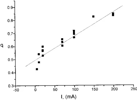
After the preparations of several PS single layers at various current densities and times, some calibration curves i.e. porosity (q), (Fig. 2.2) and formation rate of the PS layer (µm/s)TP
1
PT
, (Fig. 2.3) as a function of the current intensity (I) were obtained.
Fig. 2.2. Dependence of the porosity q (varying from 0 to 1) as a function of the current intensity for our PS samples.
We recall that the average current density, J (mA/cmP
2
P
), is obtained dividing the current intensity, I (mA), by the surface area (in our case 6.16 cmP
2 P ) of the Si samples. TP 1 PT
32
Fig. 2.3. Dependence of the porous layer growth rate from the current intensity applied during the electrochemical reaction of PS formation beginning from pP
+
P
-type crystalline Si, doped B, of 0.01 Ωcm resistivity.
The thickness was determined by: cross section SEM, weight loss measurements and IR or visible reflection spectra (see successive chapter).
Once defined the relation among the process parameters (J and t) and the characteristics of the produced PS layer, they have been used for preparing PS samples with well-established properties (both single layers and multilayer systems).
2.2 SAMPLES POST-TREATMENTS
U
2.2.1 Oxidation
For better comparing the results of the oxidizing processes, every sample has been cut in four parts, each of them was then separately treated with air saturated with vapors of HB2BO of different liquid organic substances at RT. The liquids were poured in a glass and that was inserted inside a glass bell, acting as a sort of reaction chamber (Fig. 2.4). After two hours, when the environment was considered saturated, the PS sample was introduced (movement showed by the arrow in the left side of Fig. 2.4), having care to perturb as little as possible the equilibrium formed inside the chamber. The samples have been kept in contact with the saturated vapors, for predefined times. The induced oxidation was then studied by FTIR spectroscopy.
33
Fig. 2.4. System used for the oxidation studies in various saturated atmospheres. (a) is the glass chamber that contains the saturated environment; (b) is the glass that contains the liquid used for the oxidation; the arrow (c) indicates the movement of the samples in and out of the chamber.
U
2.2.2 Functionalization
Generally PS samples are first produced by the classical electrochemistry process and then functionalized following various post-treatment procedures. The PS samples are derivatized by the contact with the molecules of pure liquids or present in a solution. The functionalization reaction can develop in various conditions:
• Under white or UV, light Irradiation of variable intensity for times ranging from 30 min to few hours;
• At high temperature, refluxing the PS sample in the liquid;
• In presence of chemical catalyzer e. g. Lewis acids in the liquid for suitable times.
During our activity, we have first tested the above mentioned function procedures, then, we have developed a new in-situ PS formation-functionalization method. This new method consists in putting the molecules to be chemisorbed directly in the solution used for the PS formation reaction. The time duration of the functionalization reaction is that of the PS formation process: from few seconds to several minutes according to the desired thickness of
(a)
(b)
34
the porous layer. The percentage of functionalization depends on the concentration of organic substance in the solution.
The method and its peculiarities will be described in details in next chapter.
2.3 SAMPLES CHARACTERIZATION
U
2.3.1 Gravimetric Analysis
By gravimetric measurements it is possible to determine the porosity and the thickness of a PS layer, although it is a destructive technique.
The porosity is defined as the fraction of void within the PS layer and can be determined easily by weight measurements with an accuracy of about 1%. The virgin wafer is first weighed before anodization (mB1B), then just after anodization (mB2B) and finally after dissolution of the whole porous layer in a molar NaOH aqueous solution (mB3B).
Uniform and rapid stripping in the NaOH solution is obtained when the PS layer is covered with a small amount of ethanol which improves the infiltration of the aqueous NaOH in the pores.
The porosity (q) is given simply by the following equation:
q (%) = (m
B1B- m
B2B)/ (m1- m
B3B) *100.
From these measured masses, it is also possible to determine the thickness (d) of the layer according to the following formula:
d = (m
B1B- m
B3B)/(S*r)
where r is the density of the bulk Si and Sis the wafer area exposed to HF during anodization.
U
2.3.2 SEM analysis
The produced PS samples have been analyzed on the surface and on the cross section by scanning electron microscopy, SEM, using an instrument Leica, Cambridge Streoscan 360 having as source of electrons a LaBB6B crystal and Field Emission SEM (FE-SEM, Leo Supra 35). The micrographies have been obtained through collection of secondary electrons using a beam of primary electrons of 20 KeV.
35
U
2.3.3 Raman spectroscopy analysis
Raman measurements were performed with a Dilor XY triple spectrometer allowing macro- and micro-Raman measurements, with a liquid nitrogen cooled charge couplet device (CCD) detector and an adapted Olympus microscope. The spectra were excited with an ArP
+
P
laser (514.5 nm or 488 nm). The laser light was focused onto a spot of 0.2 mm in diameter for macro-Raman, and 1 µm, 2 µm, 10 µm in diameter (depending on the used objective: 100x, 50x, 10x) for micro-Raman. The scattered light was not analyzed in polarization; spectral resolution was 0.5 cmP
-1
P
; lines of a Ne lamp were used for frequency scale calibration. Care has been taken to avoid the heating of the sample by using a low power density (less than 500 W/cmP
2
P
). For theoretical information see the annex B at the end of this thesis.
U
2.3.4 Fourier Transform Infrared Spectroscopy (FTIR) analysis
The IR spectroscopy is a technique based on absorption or emission of IR radiation caused from the atoms vibrations of a molecule. An IR transmission spectrum is obtained crossing a sample by a radiation and determining what fraction of the incident radiation is absorbed at particular frequency. The frequency to which every peak appears, in an absorption spectrum, corresponds to the vibration or rotation frequency of the molecules of the sample.
The emission or absorption frequency, ν, of the radiation for the transition between the energetic states EB0B, fundamental state, and EB1B, excited state, is given by the following relation:
n = (E
B1B-E
B0B)/h
where h is the Planck constant.The interactions between the IR radiation and the matter can be described in terms of changes of the molecule dipole moment associated to the vibrations or rotations.
The IR measurements were performed in reflection mode by a FTIR Biorad Spectrometer FTS-40A with dynamic alignment. The resolution was 2 ÷ 4 cmP
-1
P
in the spectra range 400 ÷ 4000 cmP
-1
P
a gold mirror was used as a reference. The IR spectra of the PS sample has been elaborated by computer to correct the instrumental effects and to obtain spectral information namely the frequency of the various present bands, their FWHM, their intensity, etc, using the “GRAMS/32” (Galactic) software.
Besides, the IR spectra treatment allowed the correction of the IR reflection spectra for the contribution due to the support (see annex C) and for the base line.
36
The experimental spectra have been finally compared with those calculated by the software Scout, [63, 64] using the Bruggeman model (see annex D). From this comparison the porosity, the thickness and the dielectric function of the measured samples have been obtained.
37
CHAPTER 3
Research Activity
In this section the original results obtained during the course of the research activity are presented and discussed.
PART I: Effect of the interaction of PS with the environment
First part is devoted to the illustration of some studies (mainly by FTIR and SFG spectroscopy) regarding the effect of the interaction of PS single layers and superstructures with the environment. The controlled oxidation of PS in humid air accelerated by the presence of various organic molecules (Pyridine, Picoline, Lutidine, Ethylamine, Diethylamine, Triethylamine) will be presented. Finally also the case of a dosimeter of urotropin vapors will be discussed. In the second part the functionalization by different procedures of PS layers in view of application of the material as a sensor and biosensor will be illustrated.
3.1 STUDY OF THE INDUCED OXIDATION IN AIR OF PS IN
PRESENCE OF PYRIDINE VAPOR
We have studied the interaction of chemical species, from both vapor and liquid phases, with PS because this is of great importance to elucidate several aspects of the surface properties of this material, such as surface adsorption, chemical reactivity, oxidation process, surface functionalization, that are also relevant for all the possible technological applications of PS especially in the sensing field [1, 15, 25].
Recently we have studied the fast oxidation induced in PS layers by the exposure to air with saturated vapors of organic bases. Further work has been carried on to complete an FTIR study of porous silicon layers exposed to humid air with and without pyridine vapors at room temperature.
Oxidation processes can strongly influence the properties of porous silicon (PS) material. The oxidation of porous silicon (PS) has been matter of extensive studies in the past years. Intentional oxidation is used to stabilize the PS properties through the formation of passivating surface oxide layers. Moreover, there is a large interest in Si/SiOB2B systems in view of new applications in the field of opto-electronics [2]. In this work, with the aim of a better understanding of this oxidation process, we discuss the results of an FTIR study of PS samples
38
exposed to humid air with and without pyridine vapor at room temperature in the time range from 0.1 to 10,000 min (300 h). The oxidation has been followed by recording the time evolution of the IR absorption intensities of the main species involved in the process, namely: Si-HBxB, OByB Si-HBxB, Si-OH and Si-O-Si. We found that in the presence of pyridine the oxidation is much faster. The PS samples were prepared by partial anodic dissolution of pP
+
P
Si (100) wafers, with a resistivity of 0.01 Wcm, in an electrochemical cell containing a HF (50%) ethanoic solution (1:2 by volume). The cathode was an Au wire and the current density was 100 mA/cmP
2
P
. The produced samples were mesoporous PS layers with 68% porosity and thickness around 0.7 mm. They were introduced in a chamber containing air saturated with water vapor or air (relative humidity 25-30%) saturated with pyridine vapors. The temperature was kept at around 24 °C. After different exposure times ranging from few seconds to 12 days, the FTIR reflection spectra of the PS samples were measured ex-situ. Care was taken to minimize the perturbation of the open atmosphere in getting the samples in and out of the chamber.
The experimental conditions were: angle of incidence 20°, spectral range 500 –4000 cmP
-1 P and resolution 4 cmP -1 P .
First we consider the case of PS exposed to air saturated with water vapor at RT. With increasing the exposure time (tBeB), the infrared spectrum evolves as exemplified in Fig. 3.1.
Fig. 3.1. FTIR reflection spectra of a PS sample exposed at RT to air saturated with water vapor for 0 min (a), 3880 min (b) and 12372 min (c). The vertical lines indicate the positions of the main bands: OByBSi-HBx B(1), Si-HBxB (2) and
39
For the sample as prepared (tBeB = 0) the main absorption bands are due to the Si-H vibrations of SiHBxB (Si-H stretching in SiH at 2080 cmP
-1
P
and in SiHB2B at 2106 cmP
-1
P
), as expected for the hydrogen terminated PS surface. With increasing tBeB the reflection minimum due to the interference moves to higher frequency owing to the reduction of the effective refractive index of the PS layer due to the substitution of Si with silicon oxide. Besides, new bands appear and the relative intensities of all the bands change. Strong silicon oxide absorption bands appear in the region 950 – 1250 cmP
-1
P
(that includes the bulk as well the surface Si-O-Si stretching vibrations [63]) and their intensity increases with the exposure time. In the region 2100 – 2300 cmP
-1
P
, bands attributable to the Si-H stretching for silicon back-bonded to oxygen atoms, OByBSiHBxB (Si-H stretching in OSiHB3B at 2136 cmP -1 P , in OB2BSiHB2B at 2200 cmP -1 P and in OB3BSiH at 2249 cmP -1 P [65]), grow up. In the 3000 – 3700 cmP -1 P
region weak and broad bands due to the O-H vibrations also appear (inset in Fig. 3.1). While the intensities of all the above mentioned new bands tend to increase with tBeB, the Si-H stretching bands due to the original H terminated PS surface have opposite trend.
A complete set of time dependencies for the mentioned species is summarized in Fig. 3.2 where the total integrated absorption intensities, obtained by spectral treatments and by adding the contributions of all the bands present in the specific spectral regions mentioned above, are reported as a function of tBeB. te (min) 1 10 100 1000 10000 I (a .u .) 0 2 4 6 8 10 12 14 16 18 te(min) 0 5000 10000 15000 20000 I (a.u. ) 0 1 2 3 4 5 6 te (min) 1 10 100 1000 10000 I ( a .u. ) -1 0 1 2 3 4 5 6 7 8 te(min) 1 10 100 1000 10000 I ( a .u .) 0 1 2 3 (a (b) (c (d) I II III Si- OByB Si-Si-O-Si Si-(OH)BxB