Amorphous Silicon Solar Cells obtained by Hot-Wire Chemical Vapour Deposition
3. a-Si:H to nc-Si:H transition
Improved performance has been attributed to a-Si:H deposited near the transition to nc-Si:H. In this chapter, the influence of different deposition parameters on the crystallinity of the material, and consequently, on its optoelectronic properties, is analysed. The transition from a-Si:H to nc-Si:H is studied after variation of either the filament temperature, the process pressure or the hydrogen dilution. Finally, the mechanisms leading to the observed microstructural changes are discussed.
3.1. a-Si:H on the onset of microcrystallinity
The beneficial role of hydrogen dilution in PECVD deposited a-Si:H has been widely accepted since observations of improved stability were first reported [Guha et al 1981]. Moderate hydrogen dilutions (lower than those used in PECVD) have also led to reduced defect metastability in a-Si:H obtained by Hot-Wire CVD [Bauer et al. 1998b]. Not only improved material properties have been obtained after hydrogen dilution, but also enhanced stabilized performance of a-Si:H based solar cells has been achieved in both PECVD and Hot-Wire CVD [Xu et al. 1996, Tsu et al.1997, Bauer et al. 1998, Guha et al.1999, Yue et al. 2000, Guha et al. 2003]. Thus, a-Si:H obtained just before the onset of microcrystallinity has yielded the most stable solar cells. Improved order, etching of weak bonds, and lower hydrogen content (CH) seemed to account for the observed improvement.
On the other hand, recent results on nc-Si:H solar cells grown by both PECVD and Hot-Wire CVD have also focused attention on that material obtained near the transition edge between a-Si:H and nc-Si:H [Vetterl et al. 2000, Klein et al 2002]. Furthermore, a variety of thin film silicon materials produced near the onset of crystallisation, which exhibit very promising properties, have gained interest during the last years. Thus, polymorphous silicon (pm-Si:H) [Roca i Cabarrocas et al. 1998] or protocrystalline silicon (pc-Si:H) [Koh et al. 1999, Fontcuberta i Morral and Roca i Cabarrocas, 2001] are new terms that have been recently introduced into the terminology of thin film silicon technology.
The above-mentioned results clearly point to the necessity of a clear evaluation of the effect of the different technological parameters on the crystallinity of thin film silicon
3. a-Si:H to nc-Si:H transition
layers obtained by Hot-Wire CVD. Microstructure features have been typically varied by means of properly tuning hydrogen dilution (DH) and/or substrate temperature (Ts) [Tsu et
al. 1997, Bauer et al. 1998b, Mahan et al. 2000, Han et al. 2003], though some questions arise regarding the role of other technological parameters such as the filament temperature (Tf) or the process pressure (P). In the following sections, microstructural properties as a
function of the above-mentioned parameters (Tf, P, DH and Ts) will be analysed. Substrate
temperature was kept in the range of 200ºC, except when evaluating its own influence, as this regime allows the use of low cost substrates such as polymer foils [Alpuim et al. 2000], which we expect to employ in the future. In fact, preliminary results concerning the growth of transparent conductive oxides (TCO) on plastic substrates have already been presented by our group [Escarré et al. 2004].
3.2. Influence of filament temperature
In this section, results concerning the evolution of microstructural properties of thin silicon films after Tf variation will be presented. Structural properties depend critically on the
growth precursors, which are influenced by the radicals emerging from the filament. In that sense, Tf plays a key role, as its value determines the decomposition efficiency per silane
collision (αdec) and the nature of the released radicals after the catalytic reaction.
A significant concentration of atomic hydrogen (H) near the growing surface has been identified as a critical parameter for the growth of nc-Si:H [Godet et al. 1995, Solomon and Drévillon 1993]. In fact, Hot-Wire CVD has been proved to be especially effective in the production of nc-Si:H (when compared with PECVD), as the filament itself acts as a very effective source of atomic hydrogen. This fact allows the deposition of nc-Si:H with no hydrogen dilution (differently from PECVD where a certain amount of H2 is necessary), as
we will see in this section.
As far as our study is concerned, a series of samples was grown at Tf ranging from 1600ºC
to 1800ºC, whereas DH = 0% and low substrate temperature (Ts = 200ºC) were employed.
The Tf range was selected after taking into account those limitations linked to the filament
properties. The use of too low temperatures (below 1500ºC) results in the rapid breakage of the filament due to the formation of silicides after Si atoms are bonded to metallic (M)
Amorphous Silicon Solar Cells obtained by Hot-Wire Chemical Vapour Deposition
ones (M-silicides). High Tf leads to the desorption of Si atoms, so that the surface of the
metallic wire returns to its original state. Nevertheless, at low Tf, the growth rate of the
M-silicides might be faster that the Si atom desorption one, thus leading to increased brittleness [Matsumura et al. 2004]. On the other hand, too high Tf (above 2000ºC) can
cause the incorporation of impurities in the sample [Horbach et al. 1991, Zedlitz et al. 1993] and the deformation of the wire after thermal dilatation. The mentioned Tf range is
associated to the most commonly used tungsten filaments, whereas tantalum ones, which were in fact used in this section, seem to allow lower temperatures (down to 1300ºC) [Bauer et al. 1998, Van Veenendaal et al. 2001], but suffer from thermal deformation at Tf
above 1900ºC. In summary, the deposition parameters used throughout the present section were those listed in Table 3.1.
Ts (ºC) Tf (ºC) P (mbar) φSiH4 (sccm) DH (%)
200 1600-1800 3.8×10⁻² 4 0
Table 3.1. Deposition parameters for samples deposited in the Tf series. The distance between the filament and the substrate ranged between 3 and 5 cm as an inverted basket geometry was selected.
Regarding the filament characteristics, an inverted-basket shaped Ta filament as that shown in Fig. 3.1 was employed. The distance between the filament and the substrate (df-s),
whose value plays a crucial role [Dusane et al. 1993], ranged between 3 and 5 cm for the top and bottom parts of the wire respectively, leading to a mean distance of around 4 cm.
1 cm
Figure 3.1. Inverted-basket shaped Ta filament.
Firstly, the thickness (d) and the deposition rate (rd) for samples under study were
measured (Table 3.2). Only a slight increase in rd can be appreciated as Tf varied from
1600ºC to 1800ºC, giving evidence of only slightly enhanced αdec.
3. a-Si:H to nc-Si:H transition Tf (ºC) d (µm) rd (Å/s) 1600 0.75 4.2 1650 0.75 4.2 1700 0.80 4.4 1750 0.80 4.4 1800 0.80 4.4
Table 3.2. d and rd for samples considered in the Tf series.
Structural features were first analysed by means of Raman spectroscopy, from which the crystalline fraction could be evaluated. Raman spectra as a function of Tf in the region
studied are plotted in Fig. 3.2.
350 400 450 500 550 600 650 1600 ºC 1650 ºC 1700 ºC 1750 ºC Tf = 1800 ºC Intens ity (a.u.) Raman shift (cm-1)
Figure 3.2. Raman spectra for samples deposited at different Tf showing increasing Xc as Tf was varied from 1600ºC to 1800ºC.
Raman spectra of samples grown at Tf ≥ 1750ºC exhibited a clear contribution at 520 cm-1,
indicating an important nanocrystalline character. Crystalline fractions above 0.6 were obtained for these samples. On the contrary, purely amorphous layers were grown at Tf ≤ 1650ºC, for which only a broad band around 480 cm-1 could be distinguished.
Regarding that sample deposited at intermediate filament temperatures (Tf = 1700ºC), a
Amorphous Silicon Solar Cells obtained by Hot-Wire Chemical Vapour Deposition
Consistent results were obtained by FTIR spectroscopy as seen in Figure 3.3. A dominant contribution around 2000 cm-1 was observed for samples deposited at T
f ≤ 1650ºC,
pointing to an important fraction of hydrogen atoms bonded in monohydride bonds, SiH, and surrounded by a dense network. On the other hand, an increasing contribution around 2100 cm-1 was obtained for samples grown at Tf ≥ 1700ºC, indicating the presence of
either multihydride (SiH2 or SiH3) or monohydride bonds in a porous structure. The
important contribution around 2100 cm-1 has been commonly associated to low-quality a-Si:H or nc-Si:H, as most hydrogen atoms in nc-Si:H are bonded at grain boundaries, where they are on the surface of crystallites facing intergrain voids. Besides, CH, deduced
from the absorption band at 630 cm-1, decreased from ~ 12% to ~ 7% as Tf ranged from
1600 to 1800ºC, this being an additional indication of crystalline growth [Han et al. 2003].
2300 2200 2100 2000 1900 1200 1000 800 600 1600ºC 1650ºC 1700ºC 1750ºC Tf = 1800ºC Wavenumber (cm-1) Transmit tance (a.u.)
Figure 3.3. FTIR spectra for samples deposited at different Tf showing increasing contribution at 2100 cm-1 and decreasing C
H as Tf was varied from 1600ºC to 1800ºC. Both Raman and FTIR spectra showed that the Tf variation was enough to clearly affect
the microstructural properties. Moreover, it is worth remarking that equivalent results were observed when either electrical or optical properties were considered (Fig. 3.4). Both the activation energy (EA) and the dark conductivity at room temperature (σd) were coherent
with the structural characterization, as they also attested the existence of a transition as Tf
approached 1700ºC. However, electrical properties at 1700ºC seemed to be mainly dominated by the crystalline contribution, even though a measurable amorphous fraction (Xc ~ 0.12) was evidenced by Raman spectroscopy measurements.
3. a-Si:H to nc-Si:H transition 0.4 0.5 0.6 0.7 0.8 0.9 E A (eV) 1600 1650 1700 1750 1800 10-10 10-9 10-8 10-7 10-6 10-5 Tf (ºC) σ d ( Ω -1 cm -1 ) 1600 1650 1700 1750 1800 1.0 1.2 1.4 1.6 1.8 Tf (ºC) E g (e V ) a) b)
Figure 3.4. Electrical properties (a) and optical band gap (b) of thin silicon films as a function of Tf.In the transition zone, both amorphous and nanocrystalline optical absorption edges were observed.
In order to clarify the electrical behaviour observed at intermediate filament temperatures, a typical TEM image corresponding to a two-phase material is presented in Figure 3.5.
50 nm
Figure 3.5. TEM image of a two-phase material where crystallites (dark grey spots)
are embedded in an amorphous tissue (light grey).
The relationship of the mean distance between crystallites and the diffusion length of carriers plays a very important role when determining the electrical properties of the material. Crystalline properties can be observed when crystallites are close enough, which
Amorphous Silicon Solar Cells obtained by Hot-Wire Chemical Vapour Deposition
seemed to be our case at Xc values as moderate as 0.12. Conversely, an abrupt transition to
amorphous conduction is expected when the separation between crystalline grains becomes larger, so that conduction becomes dominated by the amorphous tissue surrounding them. Clearer insight into the observed mechanism is given by the effective medium approximation (EMA), which allows the study of the properties of inhomogeneous materials [Stroud 1975]. A simplified vision will be employed in our case just to bring some light. Thus, thin silicon films will be considered as a random mixture of both crystallites and a-Si:H spherical shaped grains exhibiting volume fractions f and 1-f respectively. More accurate studies would require the presence of a third medium (void) and the analysis of the actual geometry, that is, crystalline silicon grains embedded in an amorphous matrix. Thus, although qualitatively correlated, f and Xc can not be
quantitatively compared. Anyhow, an effective conductivity (σeff) combining the
conductivities of a-Si:H and crystallites can be extracted in this simplified case [Stroud 1975] as seen in eq. 3.1 0 2 ) 1 ( 2 + = − − + + − eff c eff c eff a eff a f f σ σ σ σ σ σ σ σ (3.1)
The conductivity of bulk single-crystal Si (c-Si) might have been expected to be used in equation 3.1 for σc, but the finite size of the microcrystallites affects σeff (as also observed
when the pseudoelectric function, ε, is evaluated [Kang et al. 2002]). Consequently, σc = 10-6 Ω-1cm-1, this value corresponding to samples with very high crystalline fractions,
was chosen. Figure 3.6 shows the evolution of σeff as a function of f, where a percolation
threshold value is observed around 0.33 in agreement with different reported results [Kovácik 1998, Stroud 1998, Shimakawa 2000]. Thus, regions (grains) exhibiting high conductivity are small and isolated at low crystalline fractions, whereas with further increase in f, these regions start to interconnect until the critical (or threshold) f is reached. At this point, high conductivity regions establish some kind of high conductivity network throughout the entire layer, thus leading to high effective conductivity [Kovácik 1998].
3. a-Si:H to nc-Si:H transition 0.0 0.2 0.4 0.6 0.8 1.0 10-10 10-9 10-8 10-7 10-6 σ eff ( Ω -1 cm -1 ) f fth
Figure 3.6. σeff as a function of f evidencing an abrupt transition around f
th.
σa = 10-10Ω-1cm-1 and σc = 10-6Ω-1cm-1 were chosen as typical values.
Regarding optical properties, Eg (Fig. 3.4(b)) exhibited a clear amorphous character for Tf
below 1650ºC, showing an average value of 1.7 eV. On the other hand, at Tf above
1750ºC, the optical properties evidenced the nanocrystalline behaviour of the samples, in agreement with their structural properties. In the transition zone, both amorphous and nanocrystalline absorption edges were observed, as the material consisted of a mixture of both phases (Xc ~ 0.12), each being dominant at a different energy range.
In order to analyse the presented results, both the SiH4 decomposition efficiency and the
nature of the released radicals must be considered. As far as αdec is concerned, only a slight
increase seemed to occur in our case, as deduced from the subtle change observed in rd
(from 4.2 Å/s at 1600ºC to 4.4 Å/s at 1800ºC). In that sense, the correlation between rd and
Tf was not as straightforward as that reported by other groups [Matsumura 1986, Horbach
et al. 1991]. The SiH4 decomposition efficiency on a metallic filament (tungsten in this
case) was first analysed by [Doyle et al. 1988], whose results pointed out a clear dependence of αdec on Tf. Some years later, a similar study was performed by [Horbach et
al. 1991] at higher Tf. Both experiments showed that high Tf led to enhanced SiH4
decomposition. Different hydrogen coverage of the wire was pointed as the main reason leading to such behaviour. Thus, high Tf values led to rapid hydrogen evaporation after
absorption of SiH4, therefore allowing the filament to be “fresh” for new SiH4 molecules.
Amorphous Silicon Solar Cells obtained by Hot-Wire Chemical Vapour Deposition
linked to αdec) increased only slightly. This result might be correlated with our deposition
parameters set and/or reactor design.
As far as the nature of the radicals emerging from the gas-filament reactions is concerned, they are known to affect the nature of the growth precursors. On one hand, some of the released species can reach the substrate without undergoing any collision, thus becoming growth precursors, whereas, on the other hand, secondary gas-phase reactions giving rise to different growth precursors can also occur [Molenbroek et al. 1997, Gallagher 2001]. Different studies identified H and Si as the radicals most effectively generated on the filament surface [Doyle et al. 1988, Duan et al. 2002b]. In fact, hydrogen can be effectively released from the wire, either as H2 or H, for Tf values as low as 1200-1300ºC. On the
other hand, Si atoms require higher energy to begin evaporating from the surface of the filament (Tf ~ 1500ºC). Higher Tf lead to enhanced production of Si until almost all Si
atoms produced from absorbed SiH4 molecules are evaporated at Tf > 1800ºC. Our results
pointed to an increased production of atomic hydrogen as Tf was raised. H production at
the filament is favoured as Tf is raised by limiting the formation of H2 after combination of
two H atoms. High Tf values lead to reduced hydrogen coverage of the surface and, though
lower energy is required to evaporate H2 than to release H, the need of proximity of two H
atoms to form H2 can only be satisfied at low Tf [Mahan 2003]. Not only enhanced
concentration of H near the growing surface is achieved at high Tf, but also the production
of high mobility species (such as SiH3) is favoured by the presence of atomic hydrogen
through the well-known reaction
H + SiH4 Æ SiH3 + H2 (3.2)
In summary, αdec changed only slightly, so that selective favoured production of H at
higher Tf seemed to be the main mechanism leading to nc-Si:H in agreement with reported
results [Bourée 2001, Jadkar et al. 2003]. In particular, increased H/SiH3 ratio between the
fluxes of atomic hydrogen and SiH3 radical on the growing surface at increasing Tf was
reported by [Abe et al. 2000]. Alternative approaches, such as the use of large area wires leading to enhanced H production were expected to favour the growth of nc-Si:H. In fact, previously performed experiments [Peiró 1999] manifested a shift towards low Tf on the
microstructure transition as the area of the filament was enlarged. Thus, two
3. a-Si:H to nc-Si:H transition
basket shaped tungsten filaments with either five or six loops were employed. Moreover, studies performed with a simple linear filament exhibiting smaller area led to purely amorphous samples for Tf as high as 1850ºC.
3.3. Influence of pressure
Pressure is expected to influence the structural properties of silicon thin films through different mechanisms. High deposition rate leading to disordered and porous material is expected as P increases. Moreover, the mean free path (λmfp) of the involved species is
affected by P, so that low λmfp is obtained at high pressures due to the increased density of
molecules in the deposition chamber. Besides, it is known that secondary reactions in gas phase, which eventually determine the nature of the growth precursors, strongly depend on the relation between λmfp and df-s [Molenbroek et al. 1997, Feenstra et al.1999].
Different wire geometries involving varying shapes and df-s were used in this work. In this
section, a detailed study was performed with an inverted-basket shaped tungsten filament (similar to that shown in Fig. 3.1). P was varied between 2.4×10⁻² and 1.9×10⁻¹ mbar
according to the position of the butterfly valve of the reactor, whereas the rest of the deposition conditions were kept constant as listed in Table 3.3. In accordance with the P range under study, λmfp ranged from ~ 2 cm at P = 2.4×10⁻² mbar to ~ 0.25 cm at
1.9×10⁻¹ mbar, as deduced from
) · · 2 /( P T kB coll mfp σ λ = (3.3)
where T is the gas temperature and σcoll is the collision cross section. A gas temperature
value of 500 K and σcoll of10 Å2 were used [Perrin et al.1996].
Ts (ºC) Tf (ºC) P (mbar) φSiH4 (sccm) DH (%)
200 1640 2.4×10⁻² - 1.9×10⁻¹ 4 0
Amorphous Silicon Solar Cells obtained by Hot-Wire Chemical Vapour Deposition
Both the thickness and the deposition rate for samples under study are listed in Table 3.4, where lower rd at both ends of the pressure range under study can be observed.
P (mbar) d (µm) rd (Å/s) 2.4×10⁻² 1.6 4.4 3.8×10⁻² 2.5 6.9 9.2×10⁻² 2.3 6.4 1.1×10⁻¹ 2.7 7.5 1.9×10⁻¹ 1.4 3.9
Table 3.4. d and rd for layers analysed in the P influence study. Lower rd was measured for samples deposited at both the lowest and the highest pressures.
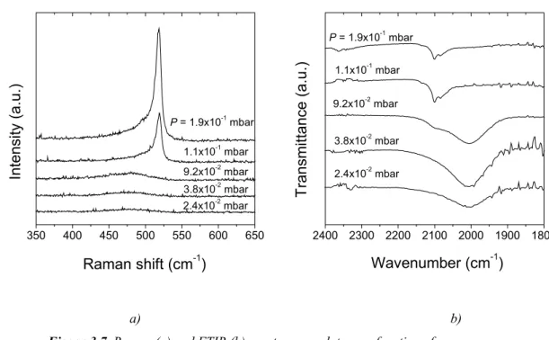
The influence of the process pressure on the structural properties was clearly manifested by both Raman and FTIR spectra (Fig. 3.7), as a clear transition from a-Si:H to nc-Si:H was observed at P ~ 1×10⁻¹ mbar. 350 400 450 500 550 600 650 2.4x10⁻² mbar In te ns ity ( a.u .) Raman shift (cm-1) P = 1.9x10⁻¹ mbar 1.1x10⁻¹ mbar 9.2x10⁻² mbar 3.8x10⁻² mbar 2400 2300 2200 2100 2000 1900 1800 2.4x10⁻² mbar T ransmit tance (a.u. ) Wavenumber (cm-1) P = 1.9x10⁻¹ mbar 1.1x10⁻¹ mbar 9.2x10⁻² mbar 3.8x10⁻² mbar a) b)
Figure 3.7. Raman (a) and FTIR (b) spectroscopy data as a function of pressure.
As already observed in the Tf study, slight variations in the parameter under study induced
very significant changes in the microstructure of the material. Accordingly, samples
3. a-Si:H to nc-Si:H transition
deposited at P = 9.2×10⁻² mbar exhibited a purely amorphous character, whereas a
significant crystalline fraction was obtained at P = 1.1×10⁻¹ mbar, thus evidencing a
remarkably abrupt transition. Regarding FTIR data, an important absorption band around 2100 cm-1 was observed at P = 1.1×10⁻¹ mbar, most probably due to the presence of
hydrogen bonds at internal surfaces (mainly crystallites). On the other hand, only the absorption peak corresponding to monohydride bonds (2000 cm-1) could be detected at P ≤ 3.8×10⁻² mbar. Furthermore, a measurable contribution around 2100 cm-1 could also be
identified for that sample grown at P = 9.2×10⁻² mbar, this being an indication of incipient
microstructural changes at increasing pressures.
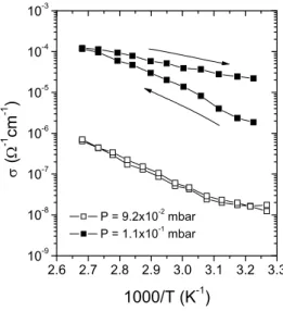
Once more, the optoelectronic properties of the material were clearly correlated with its microstructure. As an example, the Arrhenius plots of the dark conductivity corresponding to samples deposited at P = 9.2×10⁻² and P = 1.1×10⁻¹ mbar are presented in Fig. 3.8.
2.6 2.7 2.8 2.9 3.0 3.1 3.2 3.3 10-9 10-8 10-7 10-6 10-5 10-4 10-3 P = 9.2x10⁻² mbar P = 1.1x10⁻¹ mbar 1000/T (K-1) σ ( Ω -1 cm -1 )
Figure 3.8. Arrhenius plots of the dark conductivity, σ, for films deposited at
P = 9.2×10⁻² (a-Si:H) and 1.1×10⁻¹ (nc-Si:H) mbar.
The amorphous character of the sample deposited at P = 9.2×10⁻² mbar could be clearly
observed, as σd lay in the region of 10-8 Ω-1cm-1, whereas σd ~ 10-6 Ω-1cm-1 was obtained at P = 1.1×10⁻¹ mbar. On the other hand, E
A exhibited values of 0.84 and 0.61 eV for samples
Amorphous Silicon Solar Cells obtained by Hot-Wire Chemical Vapour Deposition
The deposition of nc-Si:H at high pressures might seem surprising, as low pressures are supposed to lead to a softer and gentler deposition process which might, eventually, give rise to a more ordered material. In fact, a transition from nc-Si:H to a-Si:H might not be discarded in our set-up if even higher pressures leading to very high deposition rates had been employed.
Studies dealing with the influence of P on the nature of the growth precursors have been published [Brogueira et al. 1996, Ichikawa et al. 2000]. The influence of P on the radical production is twofold. On one hand, the impingement rate of molecules on the filament can be expressed as P/ 2πmkBT [Feenstra et al. 1999], where m is the molecular mass, kB the Boltzmann’s constant, T the gas temperature, and P the working pressure. Higher production of radicals is then obtained as P is increased and, in particular, higher concentration of atomic hydrogen leading to nanocrystalline growth in accordance with [Ichikawa et al. 2000] is expected. On the other hand, P has a clear influence on λmfp,
whose relation with df-s determines the number of secondary reactions and, consequently,
the properties of the growth precursors [Dusane et al. 1993]. Experimental quantification of the importance of secondary reactions was performed by [Molenbroek et al. 1997]. Pressure was clearly observed to play a key role and, as a consequence, the product P·df-s
was first introduced as an indicator of the number of gas-phase reactions. More details concerning this issue will be given in Chapter 4.
3.4. Influence of hydrogen dilution
Direct variation of the hydrogen dilution is the most immediate approach to modify the microstructure of the material. Different groups have reported a wide range of microstructures (from purely amorphous to polycrystalline silicon) after DH changes
[Brogueira et al. 1996, Heintze et al. 1996, Alpuim et al. 1999, Peiró 1999, Brüggermann et al. 2000, Han et al. 2000, Mahan et al. 2000, Bourée 2001, Levi et al. 2003]. Atomic hydrogen is effectively produced at the hot filament surface [Jansen et al. 1989], so that lower hydrogen dilutions than those commonly employed in PECVD are required to deposit nc-Si:H. In that sense, our group reported on the growth of highly crystalline material at low Ts and elevated hydrogen dilution by means of Hot-Wire CVD back in
1994 [Cifre et al. 1994].
3. a-Si:H to nc-Si:H transition
DH, whose value was varied between 0 and 95%, is defined as shown in equation 3.4. In
our study, φSiH4 was kept constant at 4 sccm, whereas φH2 ranged from 0 to 76 sccm.
DH =φH2/(φH2+φSiH4) (3.4)
The deposition conditions for samples grown in this section are listed in Table 3.5, whereas Table 3.6 shows the corresponding thicknesses and growth rates.
Ts (ºC) Tf (ºC) P (mbar) φSiH4 (sccm) DH (%)
200 1640 3.8×10⁻² 4 0 - 95
Table 3.5. Deposition parameters for samples grown in the DH series.
φSiH4 was kept constant at 4 sccm whereas φH2 was varied between 0 and 76 sccm.
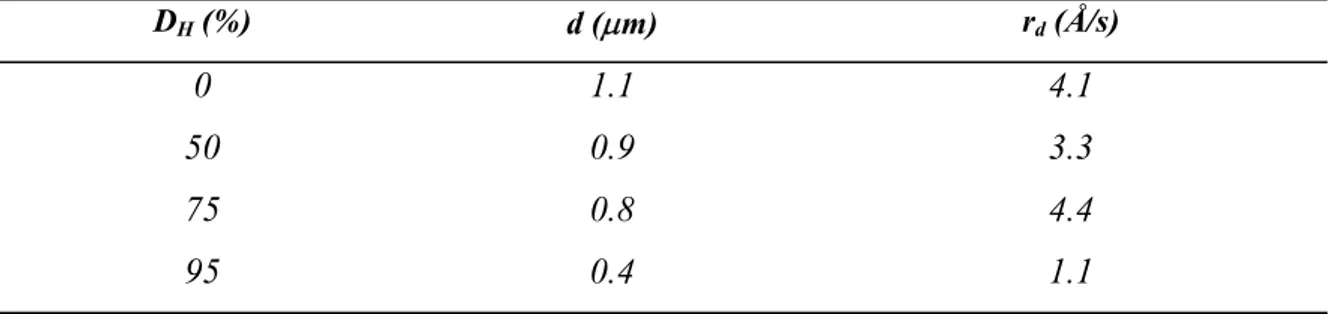
DH (%) d (µm) rd (Å/s)
0 1.1 4.1
50 0.9 3.3
75 0.8 4.4
95 0.4 1.1
Table 3.6. d and rd as a function of hydrogen dilution. A clear decrease in rd for DH = 95% is observed.
A drastic reduction in rd could be observed for that sample deposited at DH = 95%. Etching
of the growing surface due to atomic hydrogen reaching the substrate was pointed as a probable explanation for this result. Due to the etching selectivity (the etch rate of amorphous silicon by atomic hydrogen is higher than that for crystalline material), an important crystalline fraction was expected for that layer.
Raman spectroscopy results are plotted in Fig. 3.9, where the a-Si:H/nc-Si:H transition can be observed at approximately DH = 75% (Xc around 0.12). Highly crystalline material
(Xc ~ 0.65) was grown when dealing with DH above 90%, whereas no contribution around
Amorphous Silicon Solar Cells obtained by Hot-Wire Chemical Vapour Deposition 350 400 450 500 550 600 650 0 % 50 % 75 % DH = 95 % Intensity (a.u. ) Raman shift (cm-1)
Figure 3.9. Raman spectra as a function of DH. Incipient crystallinity was obtained at DH = 75%.
In order to get additional information, the electrical properties of this series of samples were also analysed (Fig. 3.10). A clear transition was observed in both σd and S for
DH ~ 75% in accordance with the microstructural properties.
0 20 40 60 80 100 10-11 10-10 10-9 10-8 10-7 10-6 10-5 DH (%) σ d ( Ω -1 cm -1 ) 100 101 102 103 104 105 106 107 S
Figure 3.10. σd and S as a function of hydrogen dilution.
A similar result to that obtained in the study concerning the influence of Tf could be also
observed. Thus, despite the moderate crystallinity obtained at DH = 75% (Xc ~ 0.12), the
3. a-Si:H to nc-Si:H transition
electrical properties seemed to be mainly determined by the crystalline phase. Therefore, and although neither σd nor S at DH = 75% were the typical ones expected for nc-Si:H,
their values showed the preponderance of the crystalline phase. Referring once more to Fig. 3.5, it seemed that the distance between crystallites was short enough as to prevent the amorphous tissue from determining the transport properties. In that sense, results reported by [Han et al. 2000] indicate that the onset of microcrystallinity is below the measurement limit of Raman spectroscopy, so that crystalline properties can be identified in optoelectronic properties even before any significant crystalline contribution appears in the Raman spectra.
In summary, and as already expected, DH was observed to lead to enhanced production of
H at the wire, so that the concentration of atomic hydrogen in the region close to the substrate was also favoured. It has been reported that the flux ratio H/SiH3 is increased
with DH, causing the transition to nc-Si:H when the flux of H is large enough [Abe et al.
2000]. Furthermore, the use of hydrogen dilution can interestingly compensate for the utilisation of low substrate temperatures, so that nanocrystalline samples can be deposited at low Ts [Alpuim et al. 1999].
3.5. Influence of substrate temperature
The influence of the substrate temperature on the crystallinity of silicon thin films was also analysed. Although low substrate temperatures (Ts ≤ 200ºC) were mainly employed in this
work, the influence of Ts was also studied to get a deeper understanding of the deposition
process. Nevertheless, only Raman spectroscopy results showing the microstructural properties of the deposited samples will be presented in this section.
The key role of H on thin silicon microstructure has been clearly demonstrated in previous sections. Anyhow, a different behaviour might be expected in this section, as two competing mechanisms coexisted in this case. On one hand, high Ts favours the surface
mobility of growth precursors, thus leading to increased order and, eventually, crystalline growth. On the other hand, low H concentrations near the growing surface are expected as Ts is increased due to H desorption, this fact contributing negatively to the surface
Amorphous Silicon Solar Cells obtained by Hot-Wire Chemical Vapour Deposition
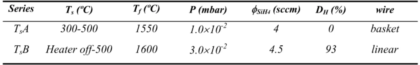
Two different technological series, whose deposition parameters are listed in Table 3.7, were studied in this section. These series allowed us to correlate both the Ts and the DH
influence on the microstructural features.
Series Ts (ºC) Tf (ºC) P (mbar) φSiH4 (sccm) DH (%) wire
TsA 300-500 1550 1.0×10⁻² 4 0 basket
TsB Heater off-500 1600 3.0×10⁻² 4.5 93 linear
Table 3.7. Deposition parameters for samples deposited in the Ts series. No hydrogen dilution was used in the first series (TsA), whereas DH ~ 93% was selected for the second one (TsB).
No hydrogen dilution (DH = 0%) was employed in the first series (TsA), for which an
inverted basket shaped Ta filament with three coils (Fig. 3.1) leading to rd values around 5
Å/s was used. In previous sections, the ability of Hot-Wire CVD to produce nc-Si:H at such growth rates was already demonstrated. Besides, only high Ts values (≥ 300ºC) were
considered in this study. Deposition conditions closer to the onset of the a-Si:H/nc-Si:H transition were employed in series TsB. In particular, relatively high DH and P values were
selected, so that a more critical dependence on Ts than in the previous series was expected.
Additionally, a linear Ta wire with df-s ~ 4 cm was used in this case, which, in combination
with the enhanced concentration of H, led to low rd values (around 1.5 Å/s). It is important
to remember that Ts values presented in Table 3.7 do not correspond to the actual
temperature of the substrate, but to the set-point temperature (Tset-point) of the controllers. Ts
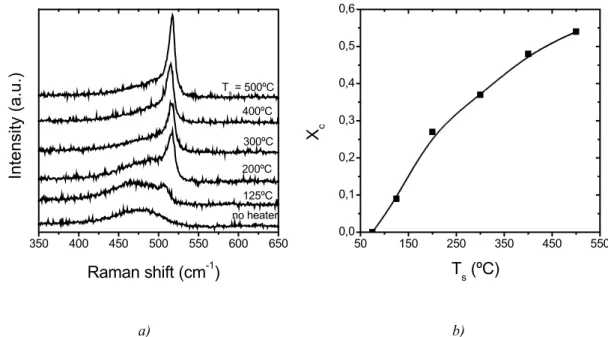
is affected by radiation from the filament, especially when dealing with its lowest values as already mentioned in Chapter 2 (section 2.1), so that our lowest temperature (with no heater) was actually around 125ºC. On the contrary, the upper limit (500ºC) corresponded in fact to Ts around 400ºC as also seen in section 2.1.
Information regarding the microstructural properties of the deposited layers was obtained by Raman spectroscopy. Purely amorphous material was obtained in series TsA (Fig. 3.11),
even when dealing with Ts as high as 500ºC. Similar results have recently been reported by
different research groups [Han et al. 2003, Levi et al. 2003]. In this case, the amount of atomic hydrogen seemed to be insufficient to allow crystalline growth, despite the surface mobility was favoured by the high substrate temperatures employed.
3. a-Si:H to nc-Si:H transition 350 400 450 500 550 600 650 Intensity (a.u.) Raman shift (cm-1) 300ºC 400ºC 350ºC 450ºC Ts = 500ºC
Figure 3.11. Raman spectra as a function of Ts for series TsA.
No crystalline growth could be observed in this series, for which DH = 0% was kept.
As far as series TsB is concerned (Fig. 3.12), a different behaviour was observed. In this
case, a clear transition to nanocrystalline growth could be observed at low Ts (125ºC), thus
evidencing enhanced surface mobility.
50 150 250 350 450 550 0,0 0,1 0,2 0,3 0,4 0,5 0,6 350 400 450 500 550 600 650 Intensity (a.u.) Raman shift (cm-1) no heater 300ºC 400ºC 200ºC 125ºC Ts = 500ºC X c Ts (ºC) a) b)
Figure 3.12. Raman spectra (a) and Xc values obtained from them (b) as a function of Ts for series TsB. Enhanced crystallinity was obtained at increasing temperatures.
Amorphous Silicon Solar Cells obtained by Hot-Wire Chemical Vapour Deposition
A DH dependent threshold for Ts in the range under study seemed to exist for the transition
a-Si:H/nc-Si:H. In particular, lower Ts values would be required at increasing DH and vice
versa [Han et al. 2003]. The evolution of Xc in this case is represented in Fig. 3.12(b),
where higher Xc values are observed as Ts was varied from “room-temperature” (Xc ~ 0)
up to 500ºC (Xc ~ 0.55). Purely a-Si:H was obtained at the lowest temperature under study,
although a large concentration of atomic hydrogen was present in the deposition chamber (DH = 93%). In fact, this DH value would have led to significant crystalline fractions if
similar filaments to those used in section 3.4 had been employed. Nevertheless, enhanced crystallinity was easily obtained at moderate Ts values, pointing to an increased surface
mobility of the growth species combining both the beneficial effect of increased Ts and a
sufficient supply of atomic hydrogen on the growing surface.
3.6. Summary
Thin silicon films with microstructural properties ranging from purely amorphous to highly crystalline (Xc > 0.65) were obtained by properly tuning the different technological
parameters. High filament temperature, pressure and/or hydrogen dilution allowed the deposition of highly crystalline material, even when dealing with relatively low substrate temperatures (Ts = 200ºC). In all cases, the enhanced production of atomic hydrogen was
pointed as the fundamental mechanism leading to increased crystallinity. Atomic hydrogen leads to selective etching of the amorphous tissue and to enhanced diffusion of precursors due to coverage of the growing surface [Solomon and Drévillon 1993, Godet et al. 1995, Brogueria et al. 1996]. Additionally, the nature of the growth precursors was also expected to play a role, with high mobility species (such as SiH3) leading to more ordered structures.
In that sense, the flux ratio of species near the substrate ([H]/[SiH3] [Abe et al. 2000] or
[H]/[SixHz] with z ≤ 3x [Brogueira et al. 1996]) has been proposed as an indicator in the
literature, with high values leading to nc-Si:H and low values driving to the deposition of a-Si:H.
It is worth reminding that, in accordance with reported results, the transition from a-Si:H to nc-Si:H was remarkably abrupt, especially when the influence of either hydrogen dilution or pressure were analysed [Feenstra 1998, Levi et al. 2003], thus evidencing the drastic influence of the studied parameters on the microstructural features. Finally, it was proved
3. a-Si:H to nc-Si:H transition
that an increase of the substrate temperature in the range under study (actual Ts ≤ 400ºC)
was insufficient to grow nc-Si:H, as long as the rest of the deposition parameters were not shifted to conditions favouring H production.
Amorphous Silicon Solar Cells obtained by Hot-Wire Chemical Vapour Deposition
4. Intrinsic a-Si:H by Hot-Wire CVD
In this chapter, the required structural, electrical and optical properties of a-Si:H layers for their application in photovoltaic devices are presented. The influence of the deposition conditions on the material quality is evaluated and our state-of-the-art material is presented. Moreover, low substrates temperatures (below 200ºC) are employed throughout the study taking into account the future use of low-cost substrates.
4.1. Device-quality intrinsic amorphous silicon
Several features are required to intrinsic amorphous silicon (a-Si:H) for its incorporation as the active layer in photovoltaic devices. Although structural, electrical and optical properties can be individually analysed by means of different characterization techniques, a clear correlation between them is observed. In this section, the required features will be briefly summarized, whereas a deeper insight will be given in the forthcoming sections. High absorption in the solar spectrum range allowing the maximum amount of electron-hole pairs to be generated is, obviously, one of the first requirements. The absorption coefficient (α) is expected to be above 3×104 cm-1 at 600 nm, whereas an optical band gap
(Eg) in the range of 1.6-1.8 eV (depending mainly on the hydrogen content and
microstructure properties) is expected. On the other hand, suitable transport properties are also required to collect the above-mentioned photogenerated carriers. Different parameters can be evaluated to determine the electrical properties of the samples, namely, the conductivity at room temperature (σd), the photoconductivity at standard illumination
conditions (σph), the photoresponse (S), or the mobility-lifetime product (µτ) of carriers.
Low σd values (σd < 1×10⁻¹⁰ Ω-1cm-1) are demanded as an indication of the absence of
electronically active impurities [Torres et al. 1996]. σd exhibits a thermally activated
behaviour, whose activation energy (EA) allows the determination of the Fermi level
position, which should be around midgap. On the other hand, σph is expected to reach high
values (above 1×10⁻⁵ Ω-1cm-1) indicating reasonably low recombination of the
photogenerated carriers. µτ can be also determined from photoconductivity experiments, thus giving additional insight into the carrier transport properties. Anyhow, and despite the
4. Intrinsic a-Si:H by Hot-Wire CVD
fact that µτ deals with the properties of both minority and majority carriers, it is known that majority carriers play a dominant role due to its much longer lifetime. In particular, µτ values above 1×10⁻⁷ cm2/V are required for device-quality material. Finally, S accounts for
the electrical behaviour of the material both under illumination and dark conditions, being values above 105 desirable for the application of the material in solar cells. As far as the specific properties of minority carriers are concerned, they are known to play a critical role on the device performance. In that sense, large diffusion length (LD > 200 nm) is needed to
allow collection. The Steady-State Photocarrier Grating technique (SSPG) allows direct insight into the diffusion length of the minority carriers.
Although the influence of optical and electrical properties can be easily understood, structural features play a very important role too. Dense and compact material is required to prevent oxidation after air exposure, which clearly limits the device performance by modifying the properties of the material. Moreover, the above-mentioned electrical and optical properties are also affected by structural features. Thus, dense and “ordered” material is desired, as it exhibits improved optoelectronic properties. The demand for “ordered” material might seem surprising when dealing with a-Si:H, so it requires further explanation. It is known that amorphous silicon lacks long-range order, but its structure is highly ordered in the short range. As a matter of fact, that local order is responsible for the relatively similar properties of both crystalline and amorphous silicon. Accordingly, different “amorphous” materials can be deposited with different degrees of disorder in the long range. The expression “ordered” material refers then to those thin film layers exhibiting an atomic structure where local order is maintained to a certain degree beyond the first neighbours. Additionally, improved stability after long time exposure to light is required to prevent degradation due to the formation of metastable defects (Staebler-Wronski effect). In that sense, enhanced stability has been associated to a-Si:H grown near the transition to nc-Si:H in the literature [Xu et al. 1996, Bauer et al. 1998b], whose structure is supposed to exhibit enhanced order.
The properties required for device-quality a-Si:H have been summarized in Table 4.1, whose numerical values have been extracted from the literature [Street 1991, Schropp and Zeman 1998]. It must be mentioned that parameters in Table 4.1 correspond to optimum material, whereas solar cells with reasonable performance have been obtained when active
Amorphous Silicon Solar Cells obtained by Hot-Wire Chemical Vapour Deposition
layers not fulfilling all the above-mentioned properties are used. In particular, the trend to increase the deposition rate (rd) and decrease the substrate temperature (Ts), which usually
implies the use of intrinsic layers with non-optimum properties, has recently focused great attention [Molenbroek et al.1997, Mahan et al. 2001, Van Veen and Schropp 2002].
Property Requirement
density high ⇒ no oxidation
Structural
properties “order” high ⇒ improved optoelectronic properties
σd low ⇒ < 10-10Ω-1cm-1 σph high ⇒ > 10-5Ω-1cm-1 Electrical properties µτ high ⇒ > 10-7 cm2/V Eg 1.6 - 1.8 eV Optical
properties absorption high ⇒ α(600 nm) > 2×104 cm-1
Table 4.1. Material properties for device-quality a-Si:H.
4.2. Our intrinsic amorphous silicon
In the following sections, structural, electrical and optical features for our state-of-the-art material will be presented. These characteristics will be compared with the properties presented in section 4.1 and, besides, the correlation between different properties will be emphasized. Details regarding the deposition conditions and their influence on the material features will be given in section 4.3. Nevertheless, and as a first approach, it is worth mentioning that filament temperatures leading to a proper H generation (Tf ~ 1600 ºC for
inverted-basket geometry), intermediate pressures (P between 1×10⁻² and 4×10⁻² mbar) and
no (or very low) hydrogen dilution led to our state-of-the-art a-Si:H. 4.2.1. Structural properties
Different observations attest the influence of microstructural properties on the behaviour of intrinsic a-Si:H layers and on the performance of solar cells. Oxidation after air exposure,
4. Intrinsic a-Si:H by Hot-Wire CVD
stability after light soaking and initial optoelectronic properties have been shown to depend on the structure of deposited layers.
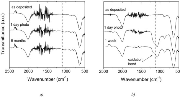
As a first requirement, high density is needed to prevent oxidation after exposure to atmosphere. Oxygen acts as an electronically active impurity that drastically worsens the transport properties of the material, so its diffusion into the bulk material must be minimized. Infrared spectroscopy measurements (FTIR) allow a direct identification of the oxygen incorporation into the film [Curtins and Veprek 1986]. Figure 4.1 shows the time evolution of FTIR spectra of two samples exhibiting different structural features.
2500 2000 1500 1000 500 Wavenumber (cm-1) 6 months 1 day photo as deposited Tr ans mi ttance (a.u.) 2500 2000 1500 1000 500 oxidation band 1 week 1 day photo as deposited Wavenumber (cm-1) a) b)
Figure 4.1. FTIR spectra of different a-Si:H layers. No oxygen incorporation was observed for our
state-of-the-art a-Si:H (a), whereas low-quality material exhibited significant oxidation after either prolonged expose to air or just one day under illumination (photo) (b).
The time evolution of the peak associated to Si-O groups clearly depended on the properties of the material. As seen in Fig. 4.1(a), samples with no detectable presence of oxygen even after several months of exposure to air were obtained. Conversely, enhanced oxidation after a few weeks or, more dramatically, after just one day under illumination, was confirmed for those samples exhibiting porous structures. Regarding measurements under illumination, impinging photons seemed to be responsible for the breaking of weak bonds (usually found in low-quality material), which eventually led to the incorporation of oxygen atoms into the growing structure.
Amorphous Silicon Solar Cells obtained by Hot-Wire Chemical Vapour Deposition
Regarding FTIR data, valuable information could also be gained from the absorption bands around 2000 and 2100 cm-1 and the calculated microstructure factor (R*) [Schropp and Zeman 1998]. R* values around 0.1-0.15 are commonly required to incorporate the material into solar cells. Nevertheless, recent results have shown the ability to grow solar cells with reasonable conversion efficiencies, even with intrinsic layers exhibiting R* between 0.2-0.3 [Van Veen and Schropp 2003]. In our case, three different spectra can be seen in Fig. 4.2, where a sample corresponding to our state-of-the-art is compared to two layers exhibiting increased disorder (all of them obtained at our laboratory).
2300 2200 2100 2000 1900 1800 c b a R*↓ Wavenumber (cm-1) Transmittance (a.u.)
Figure 4.2. FTIR spectra for a-Si:H films exhibiting different R* values. Sample “a” corresponds to our state-of-the-art material whereas “b” and “c” correspond to low-quality material deposited at
unsuitable conditions (“b” at too high pressure and “c” at too high filament temperature).
R* around 0.11 (± 0.01) was obtained for our state-of-the-art material (sample a in Fig. 4.2). The increased contribution around 2100 cm-1 observed in Fig. 4.2 for the other samples can be attributed to unsuitable deposition conditions. In this case, the use of a too high pressure (P) was responsible for the behaviour observed in sample b, whereas increased filament temperature (Tf), which in fact led to a detectable crystalline fraction
(see Chapter 3), accounted for the contribution at 2100 cm-1 observed in sample c. Additional information can be obtained from the absorption bands situated between 800 and 900 cm-1. These peaks correspond to hydrogen atoms bonded in multihydride configuration, which evidences a disordered structure. The increase of this contribution is
4. Intrinsic a-Si:H by Hot-Wire CVD
therefore related to the band centred at 2100 cm-1 as can be observed in Fig. 4.1(b), where increased absorption at 800-900 cm-1 can be appreciated for the porous sample.
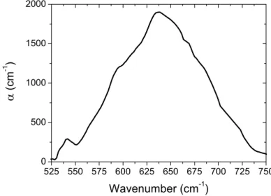
As far as the total amount of hydrogen (CH) is concerned, it can be evaluated from the
absorption peak centred on 630 cm-1 [Langford et al. 1992]. In Fig. 4.3, the absorption coefficient is presented for our state-of-the-art material. CH around 11% was observed, this
value being close to those typically observed in PECVD material [Mahan et al. 1991, Schropp and Zeman 1998]. Much lower amounts of hydrogen leading to increased stability against light soaking have been reported [Mahan et al. 1991], although high Ts were
employed (Ts > 400ºC) in those studies. Conversely, the use of low substrate temperatures
(as in our case), favours the growth of highly hydrogenated material due to less hydrogen effusion from the substrate [Smith and Wagner 1987, Mahan et al. 1991, Van Veen 2003].
525 550 575 600 625 650 675 700 725 750 0 500 1000 1500 2000 Wavenumber (cm-1) α (cm -1 )
Figure 4.3. Absorption band around 630 cm-1 for our state-of-the-art material.
Valuable information was also provided by Raman spectroscopy, as proofs of a certain structural order in a-Si:H are given by this technique. Hence, the root-mean-square bond-angle variation (∆θ) has been proposed as a measure of the degree of order [Beeman et al. 1985]. ∆θ can be analysed by the observation of the transversal optic (TO) peak, associated to the Si-Si bond, which can be observed around 480 cm-1 for amorphous material and 520 cm-1 for crystalline one. In that sense, both the width of the TO peak (Γ) and its position have been proposed as an indication of ∆θ. Different models have been suggested [Beeman et al. 1985, Vink et al. 2001], where increased order (low ∆θ values) is
Amorphous Silicon Solar Cells obtained by Hot-Wire Chemical Vapour Deposition
characterized by a narrow band (low Γ) and a shift of the peak (ωTO) toward high
frequencies. Raman spectra for both a high-quality and a low-quality layer are plotted in Fig. 4.4. 400 420 440 460 480 500 520 540 560 580 high-quality a-Si:H low-quality a-Si:H ωTO shift Γ/2 ~ 27 cm-1 Γ/2 ~ 31 cm-1 Raman shift (cm-1) Rama n In ten sity ( a. u. )
Figure 4.4. Difference observed in Raman spectra (Γ and ωTO) between device-quality a-Si:H and low quality films obtained at too high pressure (P ~ 1×10⁻¹ mbar).
As seen Fig. 4.4, Γ/2 at the high-energy side is given as a parameter instead of the full width, so that the influence of the longitudinal acoustic (LA) mode at 330 cm-1 and the longitudinal optic (LO) mode centred around 445 cm-1 can be avoided. Γ/2 below 30 cm-1
was observed for our state-of-the-art material, this value being fully comparable to those reported [Brockhoff et al. 1998, Jadkar et al. 2002]. According to different models, this Γ/2 value gives rise to ∆θ values below 8º [Tsu et al. 1984, Beeman et al. 1985]. Regarding the peak position, its dependence on the material quality can also be observed in Fig. 4.4, where a shift (5-6 cm-1) towards higher wavenumbers is observed for our optimised material. The mentioned shift can also be interpreted as a displacement towards the crystalline phase band (520 cm-1). A similar trend has been observed after hydrogen dilution [Tsu et al. 1997, Han et al. 2003b], which is known to enhance stability [Guha et al. 1981, Bauer 1998b]. Besides, reported Transmission Electron Microscopy (TEM) measurements have shown the presence of small crystallites [Brokhoff et al. 1998] or linear like objects with some degree of order [Tsu et al. 1997], which seemed to account for the frequency shift and, eventually, for the improved microstructure.
4. Intrinsic a-Si:H by Hot-Wire CVD
High values of ∆θ indicate the presence of strained bonds, which induce the formation of localized states near the band edges. These states give place to the so-called band tails in the optical absorption spectrum. Thus, a clear correlation can be found between ∆θ and the Urbach slope (Eu) [Bustarret et al. 1988b]. Moreover, localized states in the band tails can
be correlated to localized states in the mid-gap region (mainly due to dangling bonds) [Smith and Wagner 1987, Stutzmann 1989]. Optical measurements performed by means of Photothermal Deflection spectroscopy (PDS) are helpful to determine the structural order of the material through its influence on the Urbach front slope. Two different spectra are plotted in Fig. 4.5 corresponding to our state-of-the-art and to highly disordered material grown under unsuitable deposition conditions.
0.8 1.0 1.2 1.4 1.6 1.8 2.0 2.2 101 102 103 104 105 high-quality a-Si:H low-quality a-Si:H Eu ~ 53 meV Eu ~ 98 meV E (eV) α (cm -1 )
Figure 4.5. PDS measurements of a-Si:H samples with different Urbach slopes indicating different
degree of disorder. Different filament characteristics leading to different production of radicals on its surface were responsible for the change observed in this case.
Eu values around 55 meV were deduced for our state-of-the-art material from the
represented data. The obtained Eu values are acceptable and comparable to the ones
reported by other research groups [Heintze et al. 1996, Alpuim et al. 1999], though they are slightly higher than those (< 50 meV) typically associated to PECVD device-quality a-Si:H [Stutzmann 1989]. In general, Hot-Wire CVD gives rise to broader absorption curves as measured by PDS than PECVD [Alpuim et al. 1999], therefore leading to higher Eu. Nevertheless, CPM measurements, which only account for bulk properties, result in
Amorphous Silicon Solar Cells obtained by Hot-Wire Chemical Vapour Deposition
comparable Eu values for both PECVD and Hot-Wire CVD deposited samples.
Consequently, Hot-Wire CVD material seems to have a larger surface defect density than PECVD obtained one [Papadopoulos et al. 1993]. In our case, the relatively high Eu could
also be related to the use of low Ts (≤ 200ºC).
The midgap density of states due to defects in the material (mainly dangling bonds) also contributes to light absorption in the low energy range. In that sense, absorption measurements below 1.2 eV approximately have been used to calculate the density of defects in the material [Jackson and Amer 1982]. For that purpose, PDS spectra can be employed, although some drawbacks arise from its use. In particular, PDS is known to be extremely sensitive to the presence of defects at both the front surface and the layer/substrate interface [Jackson et al. 1983]. This fact results in a clear dependence of the subgap absorption on the layer thickness [Ziegler 1997], thus making it difficult to distinguish between the contributions of the bulk and the surface.
Constant Photocurrent Method (CPM) allows the determination of subgap optical absorption without taking into account superficial effects, so more reliable results are consequently expected from this technique. CPM measurements of some of our samples were performed at the Debye Institut of the Universiteit Utrecht. Comparison between CPM and PDS spectra for the same sample can be seen in Fig. 4.6.
0.8 1.0 1.2 1.4 1.6 1.8 2.0 2.2 10-1 100 101 102 103 104 α (c m -1 ) E (eV) PDS CPM
Figure 4.6. PDS and CPM measurements of an a-Si:H sample indicating different subgap absorption.
The solid line corresponds to the combination of PDS and CPM measurements. 65
4. Intrinsic a-Si:H by Hot-Wire CVD
It is important to remark that the measured sample did not correspond to our state-of-the-art material, although the clear difference between CPM and PDS in the low energy range was clearly evidenced. In fact, the sample presented in this case exhibited lower Nd values
than those observed in our best material. Unfortunately, very low photoconductivity impeded its use in photovoltaic devices. In that sense, defect densities (Nd) in the range of
5×1016 cm-3 (~1017 cm-3 as determined from PDS) were achieved for our best material, this
being a slightly higher value than that observed in device-quality a-Si:H (Nd < 1×1016 cm-3). This result is correlated with the Eu value, and could be associated with
the high value of CH (once more a consequence of the low Ts values used).
In summary, and as far as structural features are concerned, the most important results for our state-of-the-art a-Si:H are next enumerated:
1) a-Si:H resistant to oxidation diffusion after prolonged exposure to air was deposited indicating a compact structure.
2) Relatively high CH around 11% seemed to be necessary to achieve high-quality material
when keeping low substrate temperatures (Ts = 200ºC).
3) a-Si:H with quite an ordered structure was grown, i.e., low R* values (~ 0.11), narrow Raman spectroscopy bands around 480 cm-1 (Γ/2 below 30 cm-1), and E
u ~ 55 meV.
4.2.2. Electrical properties
Carrier transport properties have a dramatic influence on the solar cell performance, as proper collection of photogenerated pairs is required. The collection efficiency is affected by both the characteristics of the internal electric field (Ei) and the transport properties of
the different layers involved in the structure, especially the active one. A clear connection between disorder and localized states in the mobility gap, which reduce the transport properties of photogenerated carriers, exists. On one hand, localized states in the band tails reduce the mobility of carriers through trapping and subsequent release. A relation was already proposed in 1970 [Le Comber and Spear 1970] to correlate the drift mobility (µD)
Amorphous Silicon Solar Cells obtained by Hot-Wire Chemical Vapour Deposition
simplest case of only one energetic level for localized states (at energy E), the next expression was found
(
)
[
Ec E kT]
N N T C D =µ0 exp− − / µ (4.1)where NC and NT represent the density of extended (non-localized) and localized states
respectively near the mobility gap, and Ec corresponds to the upper limit of the mobility
edge. Similar expressions to that presented in equation 4.1 can be applied to more realistic distributions of traps. Moreover, electronic properties can be reduced dramatically by recombination mechanisms, where both an electron and a hole recombine in a deep defect state. A schematic view of the band diagram including the localized states and their effect on transport properties can be seen in Fig. 4.7.
E
CE
VE
F Recombination Localized States Trapping ReleaseFigure 4.7. Band diagram indicating the influence of localized states
on the transport properties of generated carriers.
Figure 4.8 shows σ(T) for our state-of-the-art and for a low-quality material obtained at unsuitable conditions (too high P). σd values between 5×10-11 and 2×10⁻¹⁰ Ω-1cm-1 and
activation energies between 0.8 and 0.9 eV were measured for our best a-Si:H. On the other hand, the low quality sample exhibited a too high σd value (~ 3×10⁻⁸ Ω-1cm-1). In that
sample, too high P seemed to have led to an increased void fraction, which might have resulted in the posterior oxidation. Unfortunately, oxygen is then expected to act as an electronically active impurity, thus limiting the device performance. EA is expected to be
around midgap for purely intrinsic material with no significant concentration of impurities,
4. Intrinsic a-Si:H by Hot-Wire CVD
as it corresponds to the distance between the Fermi level and the extended states band. It must be taken into account that even low impurity concentrations can significantly shift the Fermi level, thus reducing EA. That seemed to be the case in our low-quality sample, for
which EA ~ 0.46 eV was determined.
2.6 2.8 3.0 3.2 3.4 10-11 10-10 10-9 10-8 10-7 10-6
low quality a-Si:H state-of-the-art a-Si:H σ ( Ω -1 cm -1 ) 1000/T (K-1)
Figure 4.8. Temperature dependence of the electrical conductivity for
our state-of-the-art material (•) and a low quality layer ( ).
Some additional information can be gained from the shape of the Arrhenius curves. In particular, different conduction mechanisms are responsible for different regimes, which result in three temperature regions each one exhibiting a different slope [Le Comber and Spear 1970, Street 1991]. Extended state conduction is dominant at high temperatures, whereas conduction through hopping in either band tails or deep states near the Fermi level does also contribute as temperature is lowered. Thus, the evaluation of these contributions to the total conductivity gives some insight into the width of the band tails and the density of defect states in the midgap region. Nevertheless, temperatures involved in the present measurements only allowed the observation of transport through extended states. Additionally, relevant information is given by hysteresis effects [Street 1991], which are characteristic of disordered material. In that sense, two different curves are plotted in Fig. 4.9 for both low-quality and state-of-the-art material. Increased hysteresis is attributed to
Amorphous Silicon Solar Cells obtained by Hot-Wire Chemical Vapour Deposition
increased concentration of localized states in the band tails, where carriers accumulate during the heating cycle.
2.3 2.5 2.7 2.9 3.1 3.3 10-11 10-10 10-9 10-8 10-7 10-6 10-5 10-4 10-3 10-2 state-of-the-art a-Si:H low quality a-Si:H
σ ( Ω -1 cm -1 ) 1000/T (K-1)
Figure 4.9. Temperature dependence of the electrical conductivity evidencing
hysteresis effects on low-quality a-Si:H.
A relaxation process leading to the decay of the band tail carrier concentration causes the σ dependence on the thermal history of the sample. Fig. 4.10 shows the time evolution of σd
evidencing the relaxation process.
2.6 2.8 3.0 3.2 3.4 10-9 10-8 10-7 10-6 Relaxation σ ( Ω -1 cm -1 ) 1000/T (K-1) 102 103 104 105 2x10⁻⁹ 3x10⁻⁹ 4x10⁻⁹ 5x10⁻⁹ 6x10⁻⁹ 7x10⁻⁹ σ d ( Ω -1 cm -1 ) Time (s)
Figure 4.10. Time dependence of σd showing the relaxation process.
Regarding the response under illumination, Steady State Photoconductivity (SSPC) measurements were performed to determine σph. This parameter as a function of the
4. Intrinsic a-Si:H by Hot-Wire CVD
generation rate (G) was analysed using a monochromatic light (λ = 620 nm), for which a uniform generation of electron-hole pairs can be expected when dealing with 1 µm thick samples. These experiments allowed the determination of the µτ of generated carriers [Ziegler 1997, Schropp and Zeman 1998]. In Fig. 4.11, a typical σph(G) curve for our
device-quality intrinsic a-Si:H is presented. σph was approximately proportional to G for
the range under study. Nevertheless, it is known that a deviation from that behaviour can be observed when wider illumination ranges are employed, leading to a power dependence between σph and G (σph ~ Gγ). 1019 1020 10-7 10-6 Generation (cm-3s-1) σph ( Ω -1 cm -1 )
Figure 4.11. σph as a function of G for our state-of-the-art material.
From photoconductivity measurements, µτ of majority carriers could be determined from
σph = eµτG (4.2)
In the ideal case, µτ does not depend on the illumination conditions, though the above-mentioned power relation between σph and G causes µτ to vary with the generation rate. In
our case, µτ was then evaluated at G = 1021 cm-3s-1, corresponding to the expected
generation rate under one sun illumination. µτ values above 1×10⁻⁷ V/cm2 were usually
achieved for our best material, though samples exhibiting µτ as high as 1×10⁻⁶ V/cm2 were
deposited. Anyhow, these layers exhibited also relatively high σd values (~ 10-9 Ω-1cm-1),
Amorphous Silicon Solar Cells obtained by Hot-Wire Chemical Vapour Deposition
Regarding the value of σph under standard illumination conditions (G = 1021 cm-3s-1),
values above 5×10⁻⁵ Ω-1cm-1 were achieved for our best material, which is expected to be
large enough. Nevertheless, high σph values under standard illumination conditions cannot
be straightforwardly associated to device-quality a-Si:H, as they can be related to abnormally high values of σd. Therefore, both σph and σd must be jointly considered.
According to its definition, S above 105 are required [Schropp and Zeman 1998]. In our
work, S values in the range of 5×10⁵ were obtained for our state-of-the-art material
combining both high σph values and low σd values.
Finally, it must be considered that majority carriers (electrons in our case) show a major contribution to µτ [Voz 2001], so the transport features of minority carriers, which in fact limit the performance of solar cells, remain hidden. Different techniques allow the determination of minority carriers properties. SSPG deals with the ambipolar transport, which is mainly dominated by the mobility of the less mobile carriers, allowing the determination of their diffusion length (LD). Measurements performed at the Debye Institut
of the Universiteit Utrecht led to values above 200 nm for our state-of-the-art material, these values being compatible with the requirements for later implementation in solar cells.
4.2.3. Optical properties
The optical band gap (Eg) is one of the key parameters when determining the properties of
a-Si:H. Eg between 1.6 and 1.8 eV are usually found in a-Si:H, this value depending on
different material parameters, such as CH [Cody 1981, Maley and Lannin 1987, Mahan
1991] or band tail width [Yamaguchi and Morigaki 1999]. As high α is achieved at energies near the optical band gap, transmittance (T) measurements are suitable for the determination of Eg. This situation appears as opposed to the absorption in the low energy
region due to defects in the material, which gives rise to very low absorption coefficients. These low α values are best measured by means of highly sensitive techniques (PDS or CPM for example), which measure the absorptance of the sample (A). Thus, both T and A measurements must be complemented to fully acquire the optical absorption spectrum. Once T and A are measured, α over the whole range can be evaluated from
4. Intrinsic a-Si:H by Hot-Wire CVD
(
)
(
)
2 2 2 2 2 2 4 1 4 1 4 s n s n T A ns T A ns e d + − + + + + = α (4.3)where d is the thickness of the sample, and n and s are the refractive indexes of the film and the substrate respectively [Ritter and Weiser 1986, Voz 2001]. The measured absorption coefficient spectrum for one of our standard film is presented in Fig. 4.12.
0.8 1.0 1.2 1.4 1.6 1.8 2.0 2.2 100 101 102 103 104 105 E04 Hot-Wire CVD a-Si:H PECVD a-Si:H α (cm -1 ) E (eV)
Figure 4.12. α spectrum showing an abrupt increase as the energy reaches values near Eg.
Once the above-represented spectrum is obtained, different approaches can be followed to analytically determine the value of Eg. Tauc’s approach [Tauc 1974] considers parabolic
band edges, so the next expression (Tauc’s law) is proposed
) (h Eg A
hν = ν −
α (4.4)
On the other hand, if the distribution near the band edges is assumed to be linear [Klazes et al. 1982], a cubic dependence between the absorption coefficient and the energy emerges, which, in fact, seems to fit the spectrum over a wider range than the most commonly employed Tauc’s law. In this case, the so-called cubic gap is obtained from
) ( ) ( 13 g E h A hν = ν− α (4.5)