ECOC 2005 Sottomission Appendice
Optical Reconfigurable and Integrable Inverted XOR Gate based on SOA
Gianluca Berrettini (1), Alessandro Simi (2), Antonio Malacarne (1), Antonella Bogoni (3), Luca Potì (3)1 : CEIRC – Scuola Superiore Sant’Anna, Via Moruzzi 1, 56124 Pisa Italy, [email protected] 2 : Information Engineering Department, Pisa University, via Diotisalvi, 56100 Pisa, Italy,
3 : Photonic Network National Laboratory – CNIT, Via Moruzzi 1, 56124 Pisa Italy,
Abstract inverted-XOR function has been optically implemented exploiting a simple reconfigurable and integrable SOA-based scheme producing also AND, NOR and NOT gates. Performance in terms of BER for 20-ps pulsed signals at 10Gbit/s are reported.
Introduction
The development of all-optical technologies is fundamental to realize future telecommunication networks, where all the node functionalities should be carried out in the optical domain. All-optical functions such as add-drop multiplexing, packet synchronization, clock recovery, address recognition, signal regeneration are essential to avoid optoelectronic conversions, which can represent the bottleneck toward broadband and flexible networks. All-optical logic gates are key elements in the realization of such functionalities. In literature some scheme of all-optical logic gates are reported, using non linear effects in optical fibers [1] or in semiconductor devices [2-4]. In particular, Semiconductor Optical Amplifiers (SOAs) are very attractive nonlinear elements for the realization of different logic functions, since they can exhibit a strong change of the refractive index together with high gain. Moreover, differently from fiber devices, SOAs allow photonic integration.
In this paper, we propose a novel simple scheme to realize a XOR logic function, exploiting simultaneously Four Wave Mixing (FWM) and Cross Gain Modulation (XGM) in a single SOA. The same scheme, allows to implement also NOT, AND, and NOR logic gates. Bit Error Rate (BER) measurements in the case of 20 ps-signals at 10 Gbit/s confirm the high performance of the reconfigurable scheme and its suitability in long cascaded configurations.
XOR, AND, NOT
SOA BPF λ2 = λFWM BPF λ1 ≠ λFWM Pump CW NOR, NOT A B Probe
Fig. 1. Scheme of the reconfigurable logic gate. SOA-based XOR logic function
In Fig. 1 the scheme of the reconfigurable SOA-based XOR is shown. A and B are the signals that have to be processed, whose wavelengths are λA and λB
respectively. The logic function is obtained exploiting simultaneously FWM between the two polarization-aligned signals A and B, and XGM on a co-propagating probe signal, whose wavelength is the same as one of the generated FWM term
(λprobe=λFWM). The proposed scheme is able to
process both Non Zero (NRZ) or Return-to-Zero (RZ) signals. In the first case the probe is a Continuous Wave (CW) light whereas in the second case it is a pulsed clock. In order to avoid the phase interference between probe and FWM component, the probe channel is launched into the SOA with orthogonal polarization with respect to the signals and consequently to the FWM term. The signals A and B have the same input peak power, and it is high enough to saturate the device and to induce a high-efficiency FWM effect. On the other hand, the probe peak power is sufficiently low to avoid SOA saturation. Finally, a band pass filter centered at λFWM
provides the output signal for the XOR logic gate.
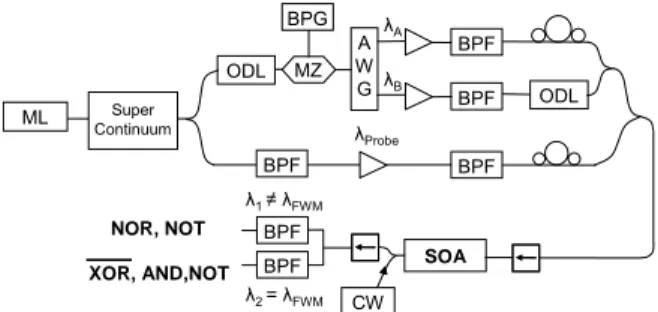
ML ContinuumSuper A W G ODL MZ BPG BPF BPF BPF ODL SOA BPF BPF λ1 ≠ λFWM λ2 = λFWM λProbe λA λB CW NOR, NOT XOR, AND,NOT BPF
Fig. 2. Experimental setup of the reconfigurable logic gate.
When both signals are present (case 11) the FWM component is generated and simultaneously the probe channel experiences a very low gain into the saturated device. After the SOA the FWM term is present, and therefore the logic gate output is at the high level. In case both signals A and B are absent (case 00) the FWM effect does not occur and the SOA is not saturated. Therefore the probe channel experiences a strong amplification, and at the filter output a high power level is present. By opportunely setting the probe channel input power it is possible to equalize the high power level at the output of the
XOR gate in the two cases 00 and 11. On the other hand if only one of the signals A and B is present (cases 10 and 01) the FWM does not occur but the SOA is saturated (the input power of only one channel is sufficient to saturate the device) strongly reducing the gain of the probe. In these cases at the output of the optical filter the power level is low. In order to avoid pattern dependent signal distortions,
ECOC 2005 Sottomission Appendice
a counter-propagating high-power CW pump has been launched into the device, decreasing the mean life time of the carriers and keeping an optimum saturation level in the SOA.
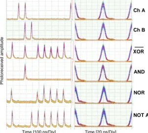
The same scheme can be exploited in order to obtain different logic gates, maintaining the same input condition for the signals A and B. In particular if the probe channel is turned off the output of the optical filter centered at λFWM represents a FWM-based logic function AND. Moreover, changing the wavelength of the probe channel so that λprobe≠λFWM allows to extract the NOR signal, using an optical band pass filter centered at λprobe. In this case, the NOR gate is based on XGM in the SOA. Finally, the NOT function can be obtained considering only one input signal in both the XOR and NOR implementation, exploiting XGM on the probe channel. Therefore the simple and integrable scheme reported in Fig. 1, which includes two different filters at the output of the SOA (or alternatively only one tunable filter), can be easily reconfigured to obtain different logic gates, just controlling the wavelength of the probe channel or turning it off. Time [100 ps/Div] Ph ot orec eiv ed ampli tu de Time [20 ps/Div] Ch A Ch B AND NOR NOT A XOR
Fig. 3. Sequences of the input signals and of the corresponding logic gate output (left) and respective eye diagrams (right).
Experimental results
In Fig. 2 the experimental setup used for the implementation of the reconfigurable all-optical logic gate is shown. An active fiber ML (Mode Locking) pulsed laser at 10GHz has been used to produce both signals and probe channel by means of supercontinuum generation. In particular the 20ps-pulsed signals A and B and the 20ps-20ps-pulsed probe are obtained from a supercontinuum in 500m of Highly NonLinear Fiber (HNLF), filtering at
λA=1550.9nm, λB=1552.5nm, and
λprobe=λFWM=1549.3nm or λprobe≠λFWM=1546.1nm. The wavelength of the counter-propagating CW pump has been fixed at 1544nm. The used semiconductor device is a commercial polarization independent bulk SOA, with small signal gain of 31dB at 1547nm. The
input average power was 3dB, -15dB, and 10dB for signals, probe and pump respectively.
In order to demonstrate the effectiveness of the proposed scheme we have considered particular bit sequences for the signals A and B at the input of the reconfigurable logic gate. We report in Fig. 3 (left) the input sequences and the corresponding output functions, using the scheme as XOR , AND, NOR and NOT respectively. In Fig. 3 (right) are also reported the eye diagrams for each implemented logic gate. -11 -10 -9 -8 -7 -6 -5 -4 1E-12 1E-10 1E-8 1E-6 1E-4 0,01 1 BER
Received peak power
BtoB chA BtoB chB AND XOR NOT NOR
Fig. 4. BER of the signals A and B back-to-back (BtoB), and of the logic gate output.
Fig. 4 shows the BER curves at the output of each logic port using the same input sequences. It can be noticed that the introduced penalty at 10-9 is lower than 0.5dB with respect to the worst input signal, making the proposed scheme suitable for long cascaded configurations. Moreover the AND logic gate presents regenerative characteristics due to the SOA saturation effect that compress the noise on the high level.
Conclusions
An all-optical XOR logic gate based on simultaneous XGM and FWM in a single SOA has been implemented using a simple and integrable scheme. The proposed gate can be reconfigured to produce also AND, NOR, and NOT logic functions. BER measurements using 20ps-pulsed signals at 10Gbit/s have shown a penalty lower than 0.5dB for each logic function, demonstrating the effectiveness of the scheme for cascaded configurations.
References
1 R. Proietti et al, proc. ECOC (2004), We4.P.115T.A.
2 Ibrahim et al. IEEE Photon. Technol. Lett., v.15, n.10, (2003), pp. 1422-1424.
3 K.E.Stubkjaer, IEEE J. Sel. Topics. Quantum Electron, v.6, n.6, (2000), pp.1428-1435.
4 H.J.S. Dorren et al, IEEE JSTQE, v.10, n.5,.(2004), pp.1079-1092.