CHAPTER 5
Integrated optofluidic microsystem based on vertical high-order
one-dimensional silicon photonic crystals
Abstract
In this work, fabrication and testing of an optofluidic microsystem exploiting high aspect-ratio, vertical, silicon/air one-dimensional (1D) photonic crystals (PhC) are reported. The microsystem is composed of an electrochemically micromachined silicon substrate integrating a 1D PhC featuring high-order bandgaps in the near-infrared region, bonded to a glass cover provided with inlet/outlet holes for liquid injection/extraction in/out the PhC-itself. Wavelength shifts of the reflectivity spectrum of the photonic crystal, in the range 1.0–1.7 µm, induced by flow of different liquids through the PhC air gaps are successfully measured using an in-plane all-fibre setup, thanks to the PhC high aspect-ratio value. Experimental results well agree with theoretical predictions and highlight the good linearity and high sensitivity of such an optofluidic microsystem in measuring refractive index changes. The sensitivity value is estimated to be 1,049 nm/RIU around 1.55µm, which is among the highest reported in the literature for integrated refractive index sensors, and explained in terms of enhanced interaction between light and liquid within the PhC.
Keywords Optofluidics · Microsystem · Photonic crystals · Refractive index
Reprinted from: G. Barillaro, S. Merlo, S. Surdo, L. M. Strambini, F. Carpignano, Integrated optofluidic microsystem based on vertical high-order one-dimensional silicon photonic crystals, Microfluid Nanofluid 2011, DOI 10.1007/s10404-011-0896-0 - license num. 2856660279718
1 Introduction
Integrated optofluidics aims at manipulating fluids and light at the microscale and exploiting their interaction to create highly versatile microsystems (Monat et al. 2007; De Stefano et al. 2007). Synergic combination of microfluidic systems and microphotonic devices opens up a number of potential applications that are mainly twofold: (a) fluids can be used to carry substances to be analyzed through highly sensitive microphotonic devices (biochemical sensing); (b) fluids can be exploited to control microphotonic devices, making them tunable, reconfigurable, and adaptive (tunable photonics). Photonic crystal (PhC) (Sakoda 2005) structures obtained by periodic arrangement of air gaps in dielectric materials provide a powerful building block for optofluidics (Monat et al. 2008; Mogensen and Kutter 2009). On one hand, PhC optical properties are very sensitive to tiny changes of the dielectric constant and thickness of the composing materials. On the other hand, injection of suitable fluids into air gaps allows PhC optical properties to be effectively modified/tuned. The generation of photonic crystals used so far for optofluidic applications has been based on planar 1D/2D structures with reduced value of the aspect-ratio (height-towidth ratio about 1), mainly due to technological limitations. A few representative examples of such a generation of optofluidic PhCs can be found in the literature (Chow et al. 2004; Lee et al. 2008; Grillet et al. 2004). Despite the noteworthy theoretical and experimental results reported in the literature on this subject, the reduced aspect-ratio limits potentialities of PhCs as optofluidic building blocks. Fluid injection into air gaps cannot be easily performed through microfluidic channels integrated on the same chip together with PhCs. Another substrate, usually the chip cover, is provided with the necessary net of channels for delivering fluids into PhC structures. Changes in the optical properties induced by fluid injection into air gaps are commonly investigated by reflection measurements using an out-of-plane readout. An in-plane readout beam cannot be easily exploited due to the reduced aspect-ratio, thus reducing on-chip optical signal routing/processing potential. Optical tuning is obtained by local modification of the refractive index at the PhC surface through fluid injection, often limiting the PhC sensitivity due to the reduced interaction length between light and fluid. Based on advantages and limitations of the up-to-date generation of PhCs, a new generation of 1D/2D PhC structures featuring high aspect-ratio can be envisioned as core element of future optofluidic microsystems and lab-on-chip with advanced features. In principle, high aspect-ratio PhCs allow both microfluidic channels and optical paths to be effectively integrated together with optical transducers (i.e. the PhC itself) on the same chip, thus envisioning on-chip manipulation/routing/processing of the optical signals before and after fluidic modification. They also allow moving light-fluid interaction from surface to bulk, so enabling deeper interaction between light and fluid and, in turn, better tuning and higher sensitivity. In particular, vertical 1D PhCs with high aspect-ratio periodic air-trenches are very appealing for the development of optofluidic
microsystems as they inherently feature independent fluidic (in the direction of the air gaps) and optical (perpendicular to air gaps) on-chip paths. Moreover, besides mere optofluidics, vertical 1D PhCs are very interesting as building block for label-free biosensors due to the possibility of using reflections from multiple periodic surfaces—instead of reflection from just a single surface as it usually happens for 1D/2D planar structures—for the detection of biological matter immobilized on the surfaces themselves.
Despite the potential of high aspect-ratio 1D/2D PhC structures for optofluidic/biosensing applications, only a few cases have been reported in the literature so far (Gruning and Lehmann 1996; Chelnokov et al. 2002; Tolmachev et al. 2002; Saadany et al. 2006; Barillaro et al. 2006; Lipson and Yeatman 2007; Mandal et al. 2009), mainly because of their more challenging fabrication with respect to planar 1D/2D PhCs. Moreover, an even lower number of papers have been published to date concerning optofluidic application of high aspect-ratio, vertical 1D PhCs (Nunes et al. 2008; Barillaro et al. 2009a). Nunes et al. (2008) reported on the fabrication of vertical silicon dioxide/air 1D PhCs for optofluidic applications by Deep Reactive Ion Etching (DRIE) trenching of a 9-µm-thick silicon dioxide layer grown by thermal oxidation of silicon substrates for 21 days at 1,075°C. The higher value of the aspect-ratio (about 3) of the fabricated PhC structure allowed microfluidic channels and waveguides to be integrated on the same chip together with the PhC itself. A maximum sensitivity value of about 800 nm/Refractive Index Unit (RIU) was claimed for such a microsystem, which is higher than sensitivities achieved with planar PhC structures (Chow et al. 2004; Lee et al. 2008; Grillet et al. 2004), thanks to the enhanced interaction between light and fluid compared to evanescence-based devices. Recently, we demonstrated that vertical silicon/air 1D PhCs with high aspect-ratio (over 30), fabricated by electrochemical micromachining (ECM) technology, featuring high-order bandgaps in the near infra-red region (wavelength range 1.0–1.7 µm), allow discriminating between liquids (ethanol and isopropanol) with a refractive index difference of the order of 10-2 through the 8 nm red-shift of the reflectivity spectrum around 1.55 µm, in good agreement with theoretical calculations (Barillaro et al. 2009a). ECM is a microstructuring technique based on the electrochemical etching of n-type silicon in hydrofluoric aqueous electrolytes (Barillaro et al. 2002a, b). This technique, which is commonly used for regular macropore formation (Lehmann and Foll 1990; Lehmann 1993), only recently has been assessed as a powerful method for fabricating silicon microstructures. ECM represents today a unique case of straightforward, low-cost wet-etching technology with microfabrication flexibility typical of complex, high-expensive dry-etching processes. Vertical high aspect-ratio (about 50) silicon/air 1D PhCs with optical high-quality surface (losses\1 dB) for optical communication applications (bandgap or reflectivity notch at 1.55 µm) fabricated by ECM have been also reported (Barillaro et al. 2008, 2010).
In this work, we demonstrate the feasibility of an optofluidic microsystem based on high-order, vertical silicon/air 1D PhCs fabricated by ECM. A micromachined silicon substrate integrating a 1D PhC micromirror is anodically bonded to a glass cover provided with inlet/outlet holes for liquid injection in the PhC air gaps. The 1D PhC micromirror is composed of 2.16-µm-thick silicon walls, separated by 5.84-µm-wide air gaps, featuring a depth of 90 µm (aspect-ratio over 40). After bonding, the microsystem is equipped with two fitting ports for an easy-to-use fluidic connection to a peristaltic pump, thus ensuring reproducible filling and withdrawing sequences. Among the advantages of such an optofluidic microsystem, with respect to planar and non-planar devices reported in the literature, there are the high uniformity of the silicon walls and the good optical quality of the surfaces; moreover, efficient coupling with the readout optical fibre is obtained in reflection. A further advantage of our assembly is related to the relaxed, single-side alignment procedure between the PhC structure and the readout optical fibre thanks to the comparable size between standard fibre diameter and silicon wall height. Experiments are performed by pumping liquids (water, ethanol, isopropanol) through the optofluidic microsystem and measuring the reflectivity spectrum in the wavelength range 1.0–1.7 µm (at normal incidence) with an optical fibre setup. As theoretically expected, insertion of liquids with increasing refractive index in the PhC structure causes a redshift of the reflectivity spectrum. Sensitivity, which is defined as wavelength shift as a function of the refractive index variation and evaluated for the reflectivity peak of different high-order bandgaps, is found to be of 1,049 nm/RIU around 1.55 µm, which is of the same order of magnitude of the best integrated refractive index sensors reported in the literature.
2 Design and fabrication of the optofluidic microsystem
The integrated optofluidic microsystem is realized by anodically bonding a micromachined silicon substrate integrating vertical, high aspect-ratio silicon/air 1D PhCs with a borosilicate glass cover provided with suitable inlet/ outlet holes through which liquid insertion into the air-gaps of the PhC can be performed. 2.1 Optofluidic section
Vertical silicon/air high-order 1D PhCs featuring a high-order bandgap around a selected wavelength λ can be designed according to the so-called hybrid quarter-wavelength stack and consist in periodic arrays of silicon layers with thickness dSi and air gaps of width dAir that must satisfy the conditions dSi = Mλ /4nSi and dAir = Nλ/4, where M and N are odd integer, independent parameters, nSi is the silicon refractive index at λ (whereas air refractive index is 1), and n = (M + N)/2 is the order of the nth bandgap, which is centred at λ (Barillaro et al. 2008). On the other hand, by choosing even integer values for M and N, 1D PhCs can be designed featuring a narrow notch, corresponding to a reflectivity minimum between two
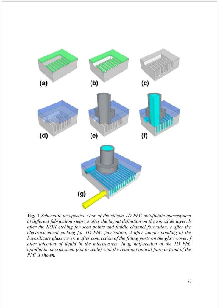
Fig. 1 Schematic perspective view of the silicon 1D PhC optofluidic microsystem
at different fabrication steps: a after the layout definition on the top oxide layer, b after the KOH etching for seed points and fluidic channel formation, c after the electrochemical etching for 1D PhC fabrication, d after anodic bonding of the borosilicate glass cover, e after connection of the fitting ports on the glass cover, f after injection of liquid in the microsystem. In g, half-section of the 1D PhC optofluidic microsystem (not to scale) with the read-out optical fibre in front of the PhC is shown.
consecutive high-order bandgaps, which can be considered as a resonance peak with high quality-factor (Q) at the selected wavelength k (Barillaro et al. 2010). In this work, vertical silicon/air 1D PhCs featuring a number of high-order bandgaps in the near-infrared region between 1.0 and 1.7 µm, among which one (namely the 17th) centred at the operation wavelength λ = 1.55 µm, are designed and fabricated. Design parameters are the silicon refractive index value nSi = 3.48, the spatial period p = 8 µm, and the porosity of the structure D = dAir/( dAir + dSi) = 0.73. The fabrication is performed by means of the ECM technology according to the process developed by Barillaro et al. (2008).
The starting material is a 675-µm-thick n-doped silicon wafer (100) oriented, with a 3–8 Ω·cm resistivity, and with a 100-nm-thick thermally grown silicon dioxide layer on its top. An array of 1-cm-long parallel straight lines, with a width of 4 µm and a pitch of 8 µm, enclosed by a squared frame is defined in the silicon-dioxide layer by means of a standard lithographic step and subsequent buffered hydrofluoric acid (BHF) etching. A quarter of the silicon die after the lithographic step and BHF etching is sketched in Fig. 1a. A potassium hydroxide (KOH) etching is used to transfer the pattern in the silicon substrate surface (Fig. 1b). The KOH etching forms full V-grooves in the straight-line area, which are used as initial seeds for silicon trenching by means of the following electrochemical etching step (Barillaro et al. 2002b, 2008), and a microchannel having trapezoidal section in the squared frame area, which surrounds the V-grooves and is exploited in optofluidic applications for filling all the trenches with suitable liquid. Electrochemical etching in a HF-based solution (HF:H2O = 5%:95% by volume, with the addition of 1,000 ppm of Sodium Lauryl Sulfate, SLS, used as surfactant) is properly controlled to produce deep regular trenches in the patterned substrate and, in turn, a vertical, high aspect-ratio silicon/air PhC micromirror (Fig. 1c). The etching voltage Vetch is set to a constant value of 3 V for the entire etching process, while the etching current Ietch is set to an initial value Ietch0 = 30.85 mA over a circular etching area of 0.66 cm2 and properly reduced during the etching in order
to obtain a constant (nominal) porosity value of 73% through the entire etching depth (Barillaro et al. 2008). This porosity value corresponds to silicon walls of 2.16 µm (M = 19 at λ = 1.55 µm) separated by 5.84-µm-thick air gaps (N = 15 at λ = 1.55 µm). The etching time tetch = 3,900 s is chosen to fully etch 90-µm-deep trenches. After the electrochemical etching, a cleaning step in HF:H2O:EtOH (10%:10%:80% by volume) aimed to the removal of the surfactant from the silicon surface and a subsequent drying step aimed to the evaporation of the liquid filling the trenches are performed.
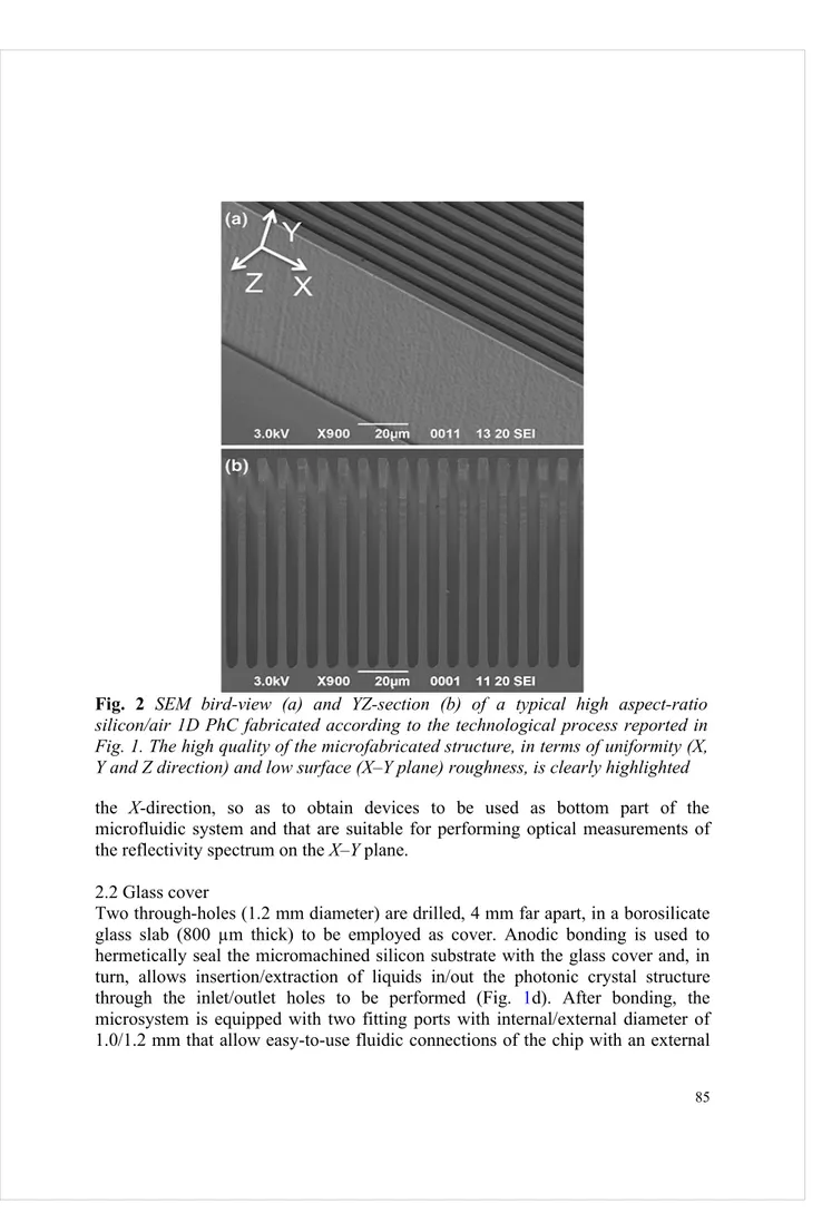
A Scanning Electron Microscope view of a typical 1D PhC fabricated according to the described technological process is reported in Fig. 2. The high quality of the microfabricated structure, in terms of uniformity (X, Y and Z direction) and low surface (X–Y plane) roughness, is clearly highlighted. As shown in Fig. 2, after the PhC fabrication process is ended, micromachined silicon substrates are cut along
Fig. 2 SEM bird-view (a) and YZ-section (b) of a typical high aspect-ratio
silicon/air 1D PhC fabricated according to the technological process reported in Fig. 1. The high quality of the microfabricated structure, in terms of uniformity (X, Y and Z direction) and low surface (X–Y plane) roughness, is clearly highlighted
the X-direction, so as to obtain devices to be used as bottom part of the microfluidic system and that are suitable for performing optical measurements of the reflectivity spectrum on the X–Y plane.
2.2 Glass cover
Two through-holes (1.2 mm diameter) are drilled, 4 mm far apart, in a borosilicate glass slab (800 µm thick) to be employed as cover. Anodic bonding is used to hermetically seal the micromachined silicon substrate with the glass cover and, in turn, allows insertion/extraction of liquids in/out the photonic crystal structure through the inlet/outlet holes to be performed (Fig. 1d). After bonding, the microsystem is equipped with two fitting ports with internal/external diameter of 1.0/1.2 mm that allow easy-to-use fluidic connections of the chip with an external
setup to be performed (Fig. 1e). As already mentioned, the trapezoidal-section microchannel distributes the liquid inserted through the fitting port in all the air trenches of the 1D PhC (Fig. 1f). The microchannel is thus closed at each end with epoxy glue in order to avoid liquid leakage during optofluidic measurements. Figure 1g shows half-section of the fabricated microsystem (not to scale) with a sketch of the read-out optical fibre in front of the 1D PhC.
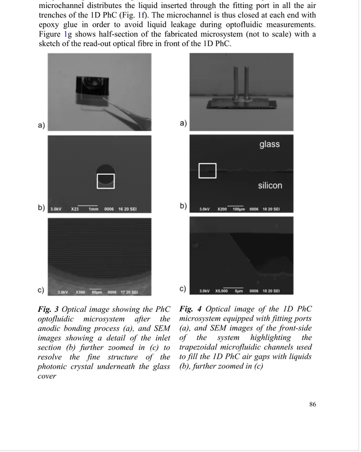
Fig. 3 Optical image showing the PhC optofluidic microsystem after the anodic bonding process (a), and SEM images showing a detail of the inlet section (b) further zoomed in (c) to resolve the fine structure of the photonic crystal underneath the glass cover
Fig. 4 Optical image of the 1D PhC microsystem equipped with fitting ports (a), and SEM images of the front-side of the system highlighting the trapezoidal microfluidic channels used to fill the 1D PhC air gaps with liquids (b), further zoomed in (c)
2.3 Microsystem assembly
Anodic bonding is a well-established, reliable, simple and inexpensive silicon packaging technique (Knowles and van Helvoort 2006). It is nowadays used for a range of material combinations (i.e. glass/silicon, glass/glass, glass/metals, etc.), device design (i.e. pressure sensors, micropumps, lab-on-chip, etc.) and applications (i.e. automotive, microfluidics, biomedical, etc.). Anodic bonding allows silicon and glass to be hermetically joined together through application of a suitable voltage (typically between 100 and 1,000 V) across the materials (silicon at the anode side) after the materials are heated up to a temperature in the range 300–500 °C. Flat (root mean square of the roughness lower than 0.05 µm), smooth and clean surfaces of both materials are required. Significantly higher values of surface roughness, surface steps or foreign contaminant particles as well as lower temperature and voltage will all prevent full-scale hermetic sealing.
The micromachined silicon substrate and glass cover are cleaned before bonding by 15 min immersion in H2SO4:H2O2 (1:1 vol), a chemical solution known as Piranha etch, so as to remove organic contaminants off the substrates. The silicon substrate is then rinsed in HF:EtOH (1:1 vol) for 2 min to remove thin oxide layer from the silicon surface. The glass cover is anodically bonded to the micromachined silicon substrate using a voltage of 600 V at the temperature of 400°C. An optical image showing the photonic crystal microsystem after the bonding process is reported in Fig. 3a, along with Scanning Electron Microscope images showing a detail of the inlet section (Fig. 3b), further zoomed in Fig. 3c to resolve the fine structure of the photonic crystal underneath the glass cover. An optical image of the assembled optofluidic 1D PhC microsystem equipped with fitting ports is shown in Fig. 4a. Figure 4b reports an SEM image of the front-side of the system highlighting the trapezoidal microfluidic channels used to fill the 1D PhC air gaps with liquids. A detail of one of the channels is reported in Fig. 4c. Evaluation of functionality
The functionality of the optofluidic microsystem is investigated by pumping different liquids (water, ethanol, and isopropanol) through the 1D PhC and measuring the reflectivity spectrum in a wide wavelength range (1.0–1.7 lm) at normal incidence and room temperature, with angle accuracy of ±1° and wavelength-steps (spectral resolution) of 0.8 nm. The optical measuring setup incorporates standard telecommunication single-mode optical fibres (SMR-28 9/125/250 µm core/cladding/coating diameter) (Barillaro et al. 2009b). Radiation from a white light source emitting in the selected wavelength range is launched into one port of a 50/50% coupler and shined onto the front face of the PhC. Radiation back reflected from the PhC is coupled back to the monochromator input of an Optical Spectrum Analyzer (OSA) for signal detection. The readout fibre is mounted on a precision micropositioner and alignment of the fibre termination in front of the PhC is monitored by means of a digital camera with a
telecentric lens, oriented at 45° with respect to the fibre axis. Good optical coupling between fibre and PhC is obtained using a tapered lensed termination characterized by a working distance of 35 µm. The alignment procedure is performed after flexible tubings are connected to the inlet/outlet fittings port. The optical alignment is not very critical since the spot diameter is 5 µm whereas the PhC is 90 µm in height. Care is just required to avoid crashing the lensed fibre tip against the PhC front face. Fluids are pumped into and extracted from the microsystem using a peristaltic pump. For each tested liquid, reflected power spectra are acquired before liquid injection (empty microsystem), when liquid has filled the PhC air gaps between the silicon walls (filled microsystem), and after liquid has been removed from the gaps.
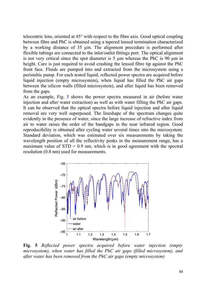
As an example, Fig. 5 shows the power spectra measured in air (before water injection and after water extraction) as well as with water filling the PhC air gaps. It can be observed that the optical spectra before liquid injection and after liquid removal are very well superposed. The lineshape of the spectrum changes quite evidently in the presence of water, since the large increase of refractive index from air to water raises the order of the bandgaps in the near infrared region. Good reproducibility is obtained after cycling water several times into the microsystem. Standard deviation, which was estimated over six measurements by taking the wavelength position of all the reflectivity peaks in the measurement range, has a maximum value of STD = 0.9 nm, which is in good agreement with the spectral resolution (0.8 nm) used for measurements.
Fig. 5 Reflected power spectra acquired before water injection (empty
microsystem), when water has filled the PhC air gaps (filled microsystem), and after water has been removed from the PhC air gaps (empty microsystem)
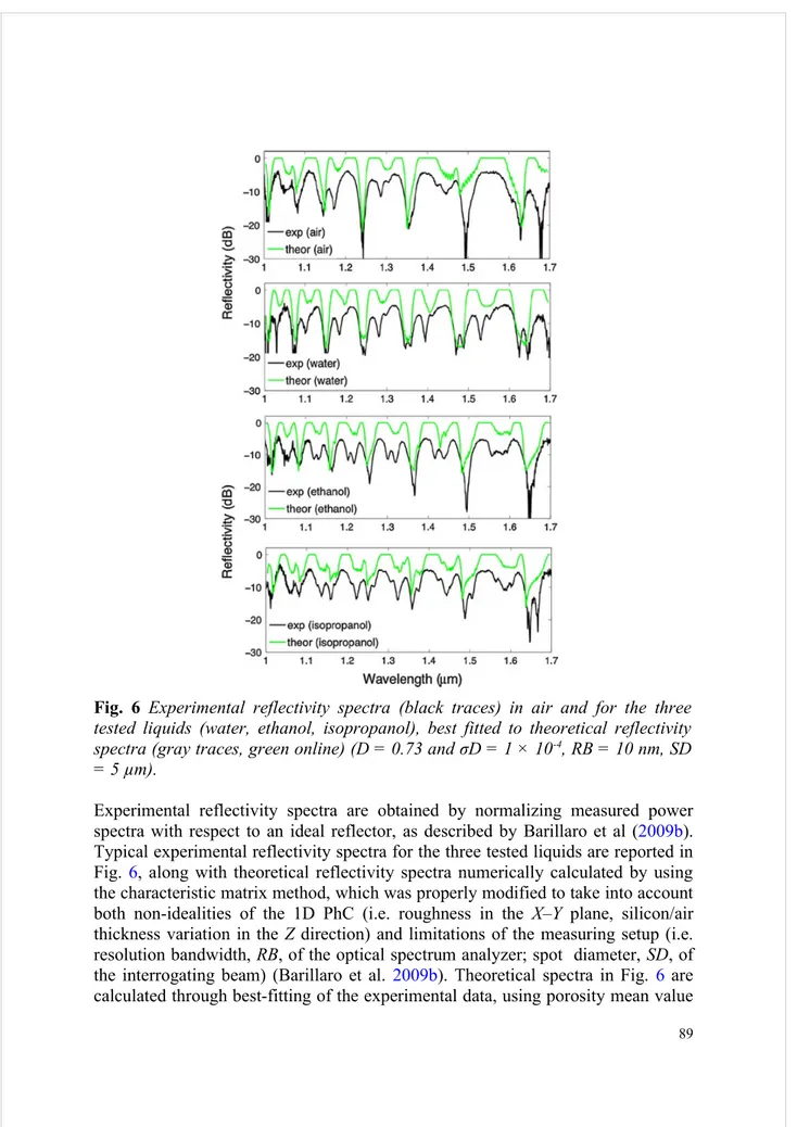
Fig. 6 Experimental reflectivity spectra (black traces) in air and for the three
tested liquids (water, ethanol, isopropanol), best fitted to theoretical reflectivity spectra (gray traces, green online) (D = 0.73 and σD = 1 × 10⁻⁴, RB = 10 nm, SD
= 5 µm).
Experimental reflectivity spectra are obtained by normalizing measured power spectra with respect to an ideal reflector, as described by Barillaro et al (2009b). Typical experimental reflectivity spectra for the three tested liquids are reported in Fig. 6, along with theoretical reflectivity spectra numerically calculated by using the characteristic matrix method, which was properly modified to take into account both non-idealities of the 1D PhC (i.e. roughness in the X–Y plane, silicon/air thickness variation in the Z direction) and limitations of the measuring setup (i.e. resolution bandwidth, RB, of the optical spectrum analyzer; spot diameter, SD, of the interrogating beam) (Barillaro et al. 2009b). Theoretical spectra in Fig. 6 are calculated through best-fitting of the experimental data, using porosity mean value
D and standard deviation σD as fitting parameters, taking into account the limited
resolution bandwidth, RB = 10 nm, employed for the measurement and the beam spot-size, SD = 5 µm. Under the hypothesis that porosity follows a Gaussian statistical distribution with mean value D and standard deviation σD, the mean
value D basically sets the spectral position of reflectivity bandgaps (high-reflectivity regions) and the standard deviation value σD essentially settles the
extinction ratio between high- and low-reflectivity regions (Barillaro et al. 2009b). According to porosity definition, the mean value D can be directly translated into silicon thickness, dSi = p(1 – D). On the other hand, the porosity standard deviation
σD can be related to the peak-to-valley amplitude of the surface roughness ρ= p3σD,
with probability 0.997. The fitting procedure yields D = 0.73 and σD = 1 × 10⁻⁴ for
the experimental reflectivity spectra of Fig. 6.
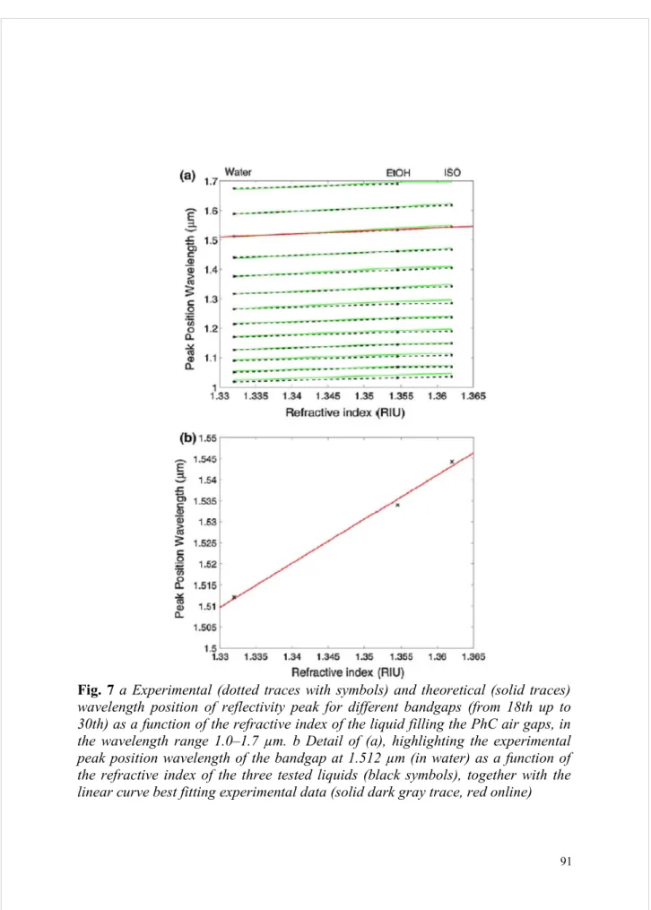
As expected, increasing the refractive index of the filling medium, from water to ethanol and isopropanol, a shift of the spectrum toward longer wavelengths is observed. In view of the application of this optofluidic microsystem as integrated refractive index sensor, we plot in Fig. 7 the peak wavelength of different bandgaps, namely from the 18th (around 1.688 µm in water) up to the 30th (around 1.028 µm in water) order, as a function of the refractive index value of the three liquids. The experimental position of each reflectivity peak is obtained after application of a numerical moving-average filter to the experimental data in order to increase the signal-to-noise ratio and, in turn, reduce the effect of measurement noise on the bandgap peak position. Experimental results (dotted traces with symbols) in Fig. 7a are in good agreement with theoretical calculations also reported in the figure (solid gray traces, green online). By best fitting the experimental curve corresponding to the bandgap at 1.512 µm (in water) with a linear relationship (solid dark gray trace in Fig. 7, red online) we obtain a sensitivity (defined as wavelength shift of the peak as a function of refractive index variation) S = dλ/dn = 1,049 nm/RIU, which is comparable to the highest value reported in the literature for integrated refractive index sensors, that is about 3,000 nm/RIU as claimed by White and Fan (2008). The use of a linear function for the experimental data fitting is fully supported by theoretical predictions, as shown in Fig. 7. An estimation of the actual limit of detection (LOD) of the proposed PhC microsystem cannot be easily performed due to both the limited spectral resolution (0.8 nm) and the high value of the OSA resolution bandwidth (10 nm) required for ensuring a sufficiently high signal-to-noise ratio and dynamics in the measurements. A worst-case estimation yields LODworst = 3 STD/S = 2.57 × 10⁻³
RIU for the bandgap at 1.512 µm (in water), which is calculated using the standard deviation maximum value STD = 0.9 nm obtained from spectral measurements above reported. A better estimation requires reducing both the spectral resolution and the resolution bandwidth, for example by using an amplified spontaneous emission source and limiting the spectral measurement to a narrow wavelength interval around the bandgap of interest.
Fig. 7 a Experimental (dotted traces with symbols) and theoretical (solid traces)
wavelength position of reflectivity peak for different bandgaps (from 18th up to 30th) as a function of the refractive index of the liquid filling the PhC air gaps, in the wavelength range 1.0–1.7 µm. b Detail of (a), highlighting the experimental peak position wavelength of the bandgap at 1.512 µm (in water) as a function of the refractive index of the three tested liquids (black symbols), together with the linear curve best fitting experimental data (solid dark gray trace, red online)
4 Conclusions
In conclusion, in this work the feasibility and functionality of an integrated optofluidic microsystem based on high-order, vertical silicon/air 1D PhCs, fabricated by electrochemical micromachining are for the first time demonstrated. In-plane read-out of the PhC spectral reflectivity is successfully performed for different liquids flowing within the microsystem, using a low coupling-loss optical-fibre setup and straightforward alignment procedure thanks to the high aspect-ratio of the PhC. Experimental wavelength shifts of PhC reflectivity spectra as a function of the refractive index of the different liquids injected in the microsystem yield a good linearity and a high sensitivity, in agreement with theoretical predictions. A sensitivity value of 1,049 nm/RIU is measured around 1.55 µm, which is comparable to the top state-of-the-art integrated refractive index sensors. A LOD worst-case of the order of 10-3 RIU is estimated from spectral
measurements, though limited by the specific parameters used for optical measurement.
Further tests will be aimed at performing an exhaustive characterization of the PhC microsystem using a larger set of refractive index values as well as estimating the actual LOD of the microsystem. Future work will be performed to obtain an optimized design of the PhC aimed at improving the microsystem sensitivity while reducing the LOD, as well as a better layout allowing read-out paths to be integrated in the silicon substrate together with the PhC structure and the fluidic channels. It is our opinion that the proposed microsystem represents a first step towards the development of a new-concept PhC optofluidic building block opening new horizons for both optofluidic microsystems and Lab-on-Chip.
Acknowledgments This research was partially supported by PRINMIUR and CARIPLO Foundation.
Reference
_________________________________________________________________
Barillaro G, Nannini A, Pieri F (2002a) Dimensional constraints on high aspect ratio silicon microstructures fabricated by photoelectrochemical etching. J Electrochem Soc 149(3):C180–C185
Barillaro G, Nannini A, Piotto M (2002b) Electrochemical etching in HF solution for silicon micromachining. Sens Actuators A 102(1–2):195–201
Barillaro G, Diligenti A, Benedetti M, Merlo S (2006) Silicon micromachined periodic structures for optical applications at 1.55 lm. Appl Phys Lett 89(15):151110–151113
Barillaro G, Strambini LM, Merlo S (2008) Bandgap tuning of silicon micromachined 1-D photonic crystals by thermal oxidation. IEEE J Sel Topics Quantum Electron 14(4):1074– 1081
Barillaro G, Merlo S, Strambini LM (2009a) Optical characterization of alcohol-infiltrated one-dimensional silicon photonic crystals. Opt Lett 34(12):1912–1914
Barillaro G, Strambini LM, Annovazzi-Lodi V, Merlo S (2009b) Optical characterization of high-order 1-D silicon photonic crystals. IEEE J Sel Topics Quantum Electron 15(5):1359– 1367
Barillaro G, Merlo S, Surdo S, Strambini LM, Carpignano F (2010) Optical quality-assessment of high-order one-dimensional silicon photonic crystals with a reflectivity notch at λ~ 1.55 µm. IEEE Photon J 2(6):981–990
Chelnokov A, David S, Wang K, Marty F, Lourtioz J-M (2002) Fabrication of 2-D and 3-D silicon photonic crystals by deep etching. IEEE J Sel Topics Quantum Electron 8(4):919– 927
Chow E, Grot A, Mirkarimi LW, Sigalas M, Girolami G (2004) Ultracompact biochemical sensor built with two-dimensional photonic crystal microcavity. Opt Lett 29(10):1093– 1095
De Stefano L, Rea I, Moretti L, Della Corte FG, Rotiroti L, Alfieri D, Rendina I (2007) An integrated pressure-driven microsystem based on porous silicon for optical monitoring of gaseous and liquid substances. Phys Stat Sol 204(5):1459–1463
Grillet C, Monat C, Smith CL, Lee MW, Tomlyenovic-Hanic S, Karnutsch C, Eggleton BJ (2004) Reconfigurable photonic crystal circuits. Laser Photon Rev 4(2):192–204
Gruning U, Lehmann V (1996) Two-dimensional infrared photonic crystal based on macroporous silicon. Thin Solid Films 276(1–2):151–154
Knowles KM, van Helvoort ATJ (2006) Anodic bonding. Int Mater Rev 51(5):273–311 Lee S-K, Park S-G, Moon JH, Yang S-M (2008) Holographic fabrication of photonic nanostructures for optofluidic integration. Lab Chip 8(3):388–391
Lehmann V, Foll H (1990) Formation mechanism and properties of electrochemically etched trenches in n-type silicon. J Electrochem Soc 137(2):653–659
Lehmann V (1993) The physics of macropore formation in low doped n-type silicon. J Electrochem Soc 140(2):2836–2843
Lipson A, Yeatman EM (2007) A 1-D photonic band gap tunable optical filter in (110) silicon. J Microelectromech Syst 16(3):521–527
Mandal S, Goddard JM, Erickson D (2009) A multiplexed optofluidic biomolecular sensor for low mass detection. Lab Chip 9(20):2924–2932
Mogensen KB, Kutter JP (2009) Optical detection in microfluidic systems. Electrophoresis 30(1):S92–S100 (and references within it)
Monat C, Domachuk P, Eggleton J (2007) Integrated optofluidics: a new river of light. Nat Photon 1:106–114
Monat C, Domachuk P, Grillet C, Collins M, Eggleton BJ, Cronin-Golomb M, Mutzenich S, Mahmud T, Rosengarten G, Mitchell A (2008) Optofluidics: a novel generation of reconfigurable and adaptive compact architectures. Microfluid Nanofluid 4(1-2):81–85 (and references within it)
Nunes PS, Mortensen NA, Kutter JP, Mogensen KB (2008) Photonic crystal resonator integrated in a microfluidic system. Opt Lett 33(14):1623–1625
Saadany B, Malak M, Kubota M, Marty F, Mita Y, Khalil D, Bourouina T (2006) Free-space tunable and drop optical filters using vertical bragg mirrors on silicon. IEEE J Sel Topics Quantum Electron 12(6):1480–1488
Sakoda K (2005) Optical properties of photonic crystals. Springer, Germany
Tolmachev A, Granitsyna LS, Vlasova EN, Volchek BZ, Nashchekin AV, Remenyuk AD, Astrova EV (2002) One-dimensional photonic crystal obtained by vertical anisotropic etching of silicon. Semiconductors 36(8):932–935
White IM, Fan X (2008) On the performance quantification of resonant refractive index sensors. Optics Express 16(2):1020– 1028