1
1. Introduction
1.1 New materials for energy conversion with solar cells
Organic materials gained broader interest for implementing in photovoltaic solar cells in the last decade,1, 2, 3 because they are typically inexpensive, easily processable and their functionality can be tailored by molecular design and chemical synthesis. Since the report of the first organic thin film solar cell in 1985 by Tang,1 several concepts have been presented using small molecules,4 conjugated polymers,5 conjugated polymer blends,3, 6 polymer-small molecule bilayers7 , 8 and blends 9,10 or combinations of organic−inorganic materials.11,12 The potential of semiconducting organic materials to transport electric current and to absorb light in the UV-visible part of the solar spectrum is due to the sp2-hybridization of carbon atoms. Organic thin films may show optical absorption coefficients exceeding 105 cm-1, which makes them good chromophores for optoelectronic applications.13
The basic working principle of efficient solid state organic solar cells is the dissociation of photogenerated excitons (the chemically bound electron–hole pair resulting from a photoinduced excitation from the valance to the conduction band of a semiconductor) at the interface between electron donor and acceptor phases by a photoinduced charge transfer process.14 Subsequently, the charge carriers have to be transported through the respective phases to the electrodes.15, 16 Some critical parameters for the photocurrent generation are therefore the light absorption in the active layer, the efficiency of the charge transfer at the interface between two immiscible components (charge and hole carrier, respectively) and the charge carrier transport properties of the materials involved.2 As the excitons in materials consisting of organic molecules are usually not very mobile, with diffusion lengths (average distance an exciton can travel before decay) in the range of 10 nm, only a small volume around the interface between donor and acceptor material is active in the photocurrent generation. A very good method to expand the charge carrier generation volume is the distribution of the donor−acceptor interface over the whole bulk of the solar cell active layer. This can be done with organic materials either by co-evaporation or casting the two materials from a common solution. The resulting solid state blend of a donor and acceptor material is called "bulk-heterojunction", its effectiveness depending on the quality of the natural dispersion of the two immiscible phases (ideally at the 10 nm level). A most promising candidate for flexible organic solar cells based on the bulk heterojunction concept consists of an interpenetrating network of a conjugated polymer and fullerene.
Bulk heterojunction solar cells can be prepared by solution processing techniques, such as spin coating, doctor blading,17screen printing18and spray coating.19 The printing technology has enabled roll-to-roll fabrication of large area flexible devices. Although the preparation of bulk heterojunction solar cells is rather simple, the operation principles are complex and their understanding requires interdisciplinary research at different fields of material science.
Solar cells based on an electrochemical mechanism (called dye-sensitized solar cells, DSSC) developed by Gratzel 20 has also been the subject of intensive investigation. The DSSC working principle is quite different from the current p–n junction photovoltaic devices. In contrast to the batter systems, where the semiconductor assume both the task of light absorption and charge carrier transport, the two functions are separated in DSSC. Light is absorbed by a sensitizer, which is anchored to the surface of a wide band semiconductor. Charge separation takes place at the interface via photoinduced electron injection from the dye into the conduction band of the solid. Carriers are transported in the conduction band of the semiconductor to the charge collector. The use of sensitizers having a broad absorption band in conjunction with oxide films of nanocrystalline morphology permits to harvest a large fraction of sunlight. Nearly quantitative conversion of incident photon into electric current is achieved over a large spectral range extending from the UV to the near IR region. Overall solar to photo conversion efficiencies (PCE) over 10% have been reached.21 While there are good prospects to produce these cells at lower cost than conventional devices, the development of extensive high output power production plants with a sizable operating lifetime is unlikely, as opposed to the solid state organic solar cells.
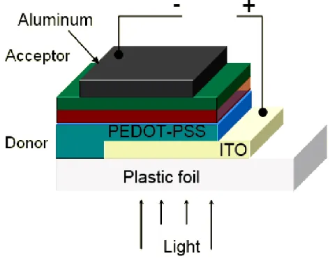
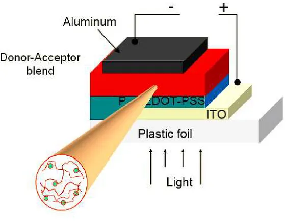
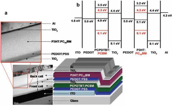
Active layers of p−n junction-type organic photovoltaic cells (OPV) loading to PCE of around 5% have been obtained using blends of poly(3-hexylthiophene) (P3HT) and [6, 6]-phenyl C61-butyric acid methyl ester (PCBM).1, 22 Heeger and co-workers have even proposed efficiencies greater than 6% with “tandem” solar cells.23 Figure 1.1, shows the structure of the multilayer polymer tandem solar cell together with the chemical structure of its components. The charge-separation layer for the front cell is a bulk heterojunction composed of poly[2,6-(4,4-bis-(2-ethylhexyl)-4H-cyclopenta[2,1-b;3,4-b']dithiophene)-alt-4,7-(2,1,3-benzothiadiazole)] (PCPDTBT) and [6,6]-phenyl-C61 butyric acid methyl ester (PCBM); that of the back cell is a bulk heterojunction composite of poly(3-hexylthiophene) (P3HT) and [6,6]-phenyl-C71 butyric acid methyl ester (PC70BM). The two polymer−fullerene layers are separated by a transparent TiOx layer and a highly conductive hole transport layer, poly(3,4-ethylenedioxylenethiophene)-polystyrene sulfonic acid (PEDOT:PSS). Electrons from the first cell combine with holes from the second cell at the TiOx-PEDOT:PSS interface. In this system,24 the TiOx layer serves five separate functions. First, hydrophilic TiOx separates the PEDOT:PSS that is cast on it from aqueous solution, from the
________________________________________________________________________________________________
3
underlying hydrophobic PCPDTBT:PCBM charge-separating layer of the front cell. However, the method of preparation of these blends suggests that there is limited control over the hetrophase topology of the photoactive material. Further optimizations of the nano and meso-structure of phase-separated electron donors and acceptors will be required to improve OPV efficiencies. Among the proposed methods to achieve such mesoscopic order, one involves using block copolymers consisting of covalently joined donor and acceptor segments.25 If the two blocks possess sufficient repulsive energy, their phase will separate into domains rich in one block or the other. The domain size, type and the topology of the interface between donor and acceptor blocks can be controlled by varying the lengths of each polymer block. Block copolymers containing a π-conjugated polymer may thus generate unique self-assembled hetrophase electronic materials with appropriate shape and size of the domains through which the photocharges may percolate to the electrodes.
Semiconducting block copolymers have been synthesized before. Of particular note are those formed using chain-end functionalized poly(phenylene vinylene)s 26,27 or poly(3-alkylthiophene)s 28 , 29 , 30
as macro-initiators for controlled radical polymerizations, or a P3HT macroinitiator for anionic polymerization.31 McCullough and co-workers prepared original semiconducting materials
a
b
Figure 1.1 (a) The device structure and TEM cross-sectional image of a polymer tandem solar cell
(b) Energy-level diagram showing the HOMO and LUMO energies of each of the component materials.23
of poly(3-hexylthiophene-b-styrene) (P3HT-b-PS) and poly(3-hexylthiophene-b-isoprene) via reversible addition fragmentation chain transfer (RAFT) and nitroxide mediated radical polymerizations (NRP) techniques, and showed the formation of nanofibrils and densely packed wires by self-assembling of these block copolymer structures.32
Among the methods available for the systems of block copolymers, the convenient scheme based on the coupling of the two pre-formed homopolymer blocks is becoming increasingly popular. A typical example is the addition of the Huisgen’s 1,3-dipolar cycloaddition-based “Click” chemistry for the production of block copolymer from end-functional homopolymers. The concept of “Click” chemistry was introduced in 2001 by Sharpless and co-workers,33 who revisited the Huisgen’s 1,3-dipolar cycloadditions34,35,36 between azido and alkynyl groups using copper salts as catalysts. It is a simple and well controlled reaction useful for building block or graft-copolymers by linking two macromolecules bearing suitable functional groups in the chain end or in the side chain, respectively.37,38,39,40 This synthetic approach presents specific advantages of considerable interest for organic semiconductors and electronics. First, it provides purer and more stable materials, properties which are of primary importance in electronics. Second, the “Click” reactions offers quantitative yields, generate inoffensive byproducts and require simple reaction procedures. Finally, this technique enables a precise control of the resulting block copolymer from well-defined end-functionalized parent homopolymers. Nowadays, a palette of living polymerization methods is available to provide such homopolymers. This approach was followed also in the present work to obtain poly(3-hexylthiophene)-block-poly(acrylonitrile) from alkynyl-terminated P3HT and azido-PAN.
A more complex but also more potentially interesting situation arises when one of the convents and bulk hetrojuncation polymer is replaced by one compound of semiconducting inorganic nanocrystals or quantum dots (QDs). In fact, their stability and surface chemistry must be accurately explored. In particular, because inorganic nanocrystals are metastable species, it has been shown that the workup and processing are strongly related to the nature and structure of the surface ligands, the interface between the organic and inorganic components, and the photochemical stability of the nanocrystal/ligand complex.
Among the various inorganic semiconducting nanoparticles or QD CdSe nanocrystals, with an electron affinity in the range 3.8−4.5 eV are suitable as electron acceptors when combined with conjugated polymers. Their band gap, as for any quantum dots is controlled simply by adjusting the size. The dispersion of QDs in the polymer matrix, however, is a critical issue due to the tendency of the inorganic nanoparticles to large aggregates. This is a particularly undesired feature if the final morphology of the nanosturcted hybrid or nanocomposite material influences the efficiency of the
________________________________________________________________________________________________
5
key process that, in our case, is the charge transfer at the polymer/QD interface. The role of the interface and its extension is thus a critical feature, as the junctions between acceptor and donor phase may contribute to the enhancement of the overall efficiencies of charge separation step in the active layer of OPV.
The role of donor−acceptor interfaces on the efficiency of photovoltaic devices implies that a number of criteria must be satisfied by the morphology of the blend for optimum solar cell performance: first, electron donor and acceptor domains must segregate into chemically homogeneous regions with typical sizes of the order of the exciton diffusion length, in order to enhance the exciton dissociation probability, thus avoiding wasteful radiative recombination events; second, donor (acceptor) domains must be continuously connected to the anode (cathode) to favor efficient charge transport. This is critical factor together with the intrinsic electron (hole) mobility within the given domain, to allow a balanced transport changes. The better is important to present local accumulation of charges.
1.2 Solar Cell Concepts
A solar cell or photovoltaic cell is a device that converts light directly into electricity by the photovoltaic effect. Sometimes the term solar cell is reserved for devices intended specifically to capture energy from sunlight, whereas the term photovoltaic cell is used when the light source is unspecified. Assemblies of cells are used to make solar panels, solar modules or photovoltaic arrays. Photovoltaic is the field of technology and research related to the application of solar cells in producing electricity for practical use.
In solar cells, the most important term is an electron donor and acceptor, and the way of preparing active layer by them. Below we can see some commonly used examples of electron donor and acceptor.
1.2.1Overview of π-conjugated polymers as electron donor
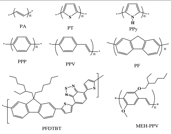
Conjugated polymers are macromolecules that possess alternating single and double bonds along the main chain. Some common conjugated polymers are poly(acetylene) (PA), poly(thiophene) (PT), poly(pyrrole) (PPy), poly(pphenylene) (PPP), poly(p-phenylenevinylene) (PPV), poly(fluorene) (PF), poly[2,7-(9,9’-dihexylfluorene)-alt-2,3-dimethyl-5,7-dithien-2-yl-2,1,3-benzothiadiazole] (PFDTBT) and poly[2-methoxy-5-(2'-ethylhexyloxy)-1,4-phenylene vinylene] (MEH-PPV) which are illustrated in figure 1.2.
* * S * N * * * * * * * H n n n n n n
PA
PT
PPy
PPP
PPV
PF
* S S N N S * O O * nPFDTBT
MEH-PPV
Figure 1.2 Structures of several common conjugated polymers
The potential use of conjugated polymers in electronic devices was realized in the late 1970s when the first electrically conductive polymer was discovered: PA doped with iodine.41 In recognition of this extraordinary discovery, the scientists (Shirakawa, MacDiarmid and Heeger) were jointly awarded the Nobel Prize (2000) in Chemistry. Many conjugated polymers that were studied in the early 1980s were based on heterocyclic compounds which were synthesized using chemical and electrochemical means.42, 43 Chemically synthesized conjugated polymers resulted in powders which were insoluble and uncharacterizable using conventional analytical techniques.42 The primary interest in these powders was their electrical conductivity and their corresponding electronic structure. Alternatively, electrochemical synthesis of conjugated polymers was a more attractive approach because films were formed on the electrode.43 Significant research on these polymer films was therefore performed to understand their spectroelectrochemical properties. In the mid 1980s, Elsenbaumer reported the novel synthesis of soluble conjugated polymers by attaching an alkyl side chain on PT. The solubility of the polymers allowed structural characterization and polymer processing using spin or drop cast methods.44, 45 ,46 To date, extensive of research on soluble conjugated polymers has been performed, due to their potential use as components in electronic applications, such as field effect transistors (FETs),46 light emitting diodes (LEDs), 47
________________________________________________________________________________________________
7
actuators,48 and solar cells.5 The development of these soluble conjugated polymers has led to significant improvement in their properties, including their electrical conductivity (up to 2000 S/cm),14, 49 field effect mobility (~0.12 cm2 V-1 s-1) with excellent on/off ratios in FETs, high solid state photoluminescent 50 and LED efficiencies (10% photons/electrons, external). Improvemens up to 6% PCE from single active layer polymer solar cells has been reported recently.5,51
P3HT is the polymer most intensively investigated as the main component of the active layer in OPV cells due to the very high hole mobility and good processability. However, the band gap of P3HT (about 2 eV) limits the range of light harvesting to about 650 nm. Therefore, the devices reported more recently have been based on low band gap homo- and co-polymers such as e.g.: poly(thiophene–co−benzothiadiazole).52
Selection of suitable polymers is also based on such properties as stability in the presence of moisture and oxygen. This requirement is reportedly matched by an alternating copolymer of bithiophene and dioctylfluorene units.53 However, the presence of octyl chains perpendicular with respect to the conjugated planes prevents close π−π
interchain stacking and is responsible for lower hole mobility than in P3HT (Table 1.1).
Table 1.1
Selected parameters for conducting polymers used in hybrid polymer–semiconductor PV cells Polymer (a) ELUMO
(eV) EHOMO (eV) Eg (eV) (b) Hole mobility (c) (cm2 V−1 s−1) Ref. P3HT (NR) −2.55 −4.65 2.1 10-5 to 10-4 54, 55 P3HT (RR) −3.0 −4.90 1.9 0.05 to 0.1 56, 57 P3OT (RR) −3.55 −5.25 1.8 56 MEH-PPV −2.9 −5.30 2.4 10-4 to 10-3 58 OC1C10-PPV −3.0 −5.26 2.86 10-6 59, 60 F8T2 −3.1 −5.50 2.4 0.01 to 0.02 61, 62 APFO-3 −3.53 −5.84 2.31 3.1×10⁻⁵ 63, 64 PCPDTBT −3.57 −5.30 1.73 0.02 65 a
(NR)= regiorandom ; (RR) = regioregular; P3HT: poly(3-hexylthiophene;, P3OT: poly-(3-octylthiophene); MEH-PPV: poly[2-methoxy-5-(2'-ethylhexyloxy)-1,4-phenylene vinylene]; OC1C10-PPV: Poly[2-(3,7-dimethyloctyloxy)-5-methoxy-p-phenylene vinylene]; F8T2: poly(9,9-dioctylfluorene-co-bithiophene); APFO-3: poly[(9,9-dioctylfluorenyl-2,7-diyl)-alt-5,5-(40,70-di-2-thienyl-20,10,30-benzothiadiazole)]; PCPDTBT: poly[2,6-(4,4-bis-(2-ethylhexyl)-4H- cyclopenta[2,1-b;3,4-b′]dithiophene)-alt-4,7-(2,1,3-benzothiadiazole)]
b
Band gap c
Hole mobility in the neutral state.
In addition to the band gap energy Eg, an additional but very important factor to be taken into account when choosing the most preferable conducting polymer as the electrodonating component of a hybrid PV cell is the position of the HOMO and LUMO energy levels with respect to the energy levels of conduction and valence bands of the second component, such as an inorganic semiconductor (Figure 1.3 and Table 1.2).
1.2.2 Overview of quantum dots as electron acceptor
QDs are nanometer-scale semiconductor crystallites. Since the size of the dots is much lower than the exciton Bohr radius (the physical distance between an electron in the conduction band of a semiconductor, and the hole it leaves behind in the valence band), the electron−hole pair in a QD is tightly confined in all three dimensions. This is known as quantum confinement, which produces a number of pronounced modifications in the optical and electronic properties of the semiconductor.
Semiconductors are often classified according to the periodic table group to which they belong. For reference purpose, in table 1.2 are listed some bulk phase physical properties of several common semiconductors, including their band gap energies, electron affinity average, exciton Bohr radii, and exciton binding energies. A closer examination of the exciton Bohr radius allows to understand that quantum confinement, because important when the size of the inorganic crystals is in the range of 1−5 nm, depending on the specific compound. In the case of CdSe, for example, a nanoparticle with the largest dimension of 5 nm would behave as a QD.
Table 1.2
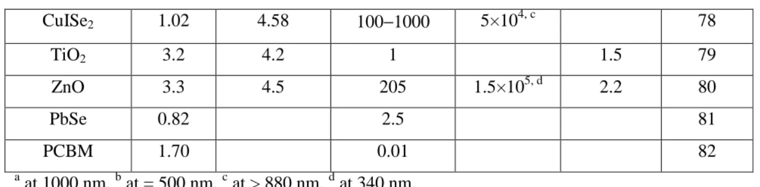
Material parameters for several common inorganic semiconductors Semiconductor (bulk material) Eg (eV) at 300K (eV) bulk electron affinity Electron mobility (cm2 V−1 s−1) at 300K Absorption coefficient (cm−1) Exciton Bohr radius (nm) Ref. Si 1.11 4.05 1500 103, a 66 CdSe 1.74 3.8−4.5 720 7×10⁴, b 6.1 67, 68, 69 CdS 2.53 4.5 200 4×10⁴, b 3.1 70, 71, 72 CdTe 1.50 4.28 1000 1.56×10⁴, b 6.5 73, 74,75 CuInS2 1.55 200 105, b 76, 77
________________________________________________________________________________________________ 9 CuISe2 1.02 4.58 100−1000 5×10⁴, c 78 TiO2 3.2 4.2 1 1.5 79 ZnO 3.3 4.5 205 1.5×10⁵, d 2.2 80 PbSe 0.82 2.5 81 PCBM 1.70 0.01 82 a at 1000 nm, b at = 500 nm, c at > 880 nm, d at 340 nm.
The structure and morphology of organic and inorganic nanoparticles, respectively that are commonly found in nanoparticle–polymer PV cells are shown in figure 1.3. The butyric acid methylester substituent of PCBM and PC71BM increases the dispersibility of the fullerene nanoparticles. The inorganic semiconducting nanoparticles (e.g, CdSe) can often be prepared in different shapes and various aspect ratios, including very high ones with rod-like or branched morphologies.83,84 The nanoparticle geometry and aspect ratio (AR) have a strong influence on PCE. Nanoparticles with ARs higher than 1 generally increase the PCE for inorganic nanoparticle– polymer PV cells. However, photoactive layers containing single wall carbon nanotube (SWNTs), which have very high AR values, give low PCE values.85 This may be suggestive of an optimum range for AR values.
1.3 Organic Solar Cells and Resources
The need to develop inexpensive renewable energy resources stimulates new approaches for the production of efficient, low cost PV devices.86 The development of organic, polymer based PV elements has introduced the possibility of obtaining cheap and easily produced energy from light.87 Organic materials have several advantages over inorganics such as lower cost and easy manufacture of thin film devices by vacuum evaporation or solution cast technologies. Organic electronic materials are conjugated molecular solids where both optical absorption and charge transport are dominated by partly delocalized π and π* orbitals.88 The flexibility of chemical tailoring of desired properties, the easy and cheap processing, and the possibility of obtaining tough free-standing thin films, makes conjugated competitive and attractivewith respect to low molecular weight organic compounds. For inorganic semiconductors, the mechanism of charge generation from incident photons is well established. In the ideal case the electronic structure consists of a conduction band and a valence band separated by an energy gap the size of which depends upon the material. When an incident visible light photon excites an electron from the valance band into the conduction band, a hole is generated in the valence band. Although a hole is simply an empty electronic state, it behaves as if it were an independent carrier of positive charge.89
Conducting polymers act also as semiconductors, their electronic properties being analogous to those of inorganic semiconductors except for their lack of dangling bonds on the surface/interfaces due to their closed shell structure. The π bonds being ideally delocalized over the entire molecule, the lower energy π orbitals (HOMO) produce the valence band and the higher energy π* orbitals (LUMO) form the conduction band. The difference in energy between band edges of the two levels produces the band gap that determines the optical properties of the material. 90
However, the charge conduction mechanism appears to be more complex for conducting polymers than for inorganic semiconductors. In general, organic semiconductors differ from the inorganic ones in the following important aspects:88
1. photogenerated excitations (excitons) are coulombically bound and do not spontaneously dissociate into separate charges in quantitative amounts;
2. charge transport proceeds by hopping between disorder-induced localized states rather than by transport within a band, which results in lower mobilities;
3. the spectral range of the optical absorption is relatively narrow compared to the solar emission spectrum (Figure 1.4);15
4. being typically macromolecules and thus one-dimensional semiconductors, their electronic and optical properties can be highly anisotropic.
________________________________________________________________________________________________
11
Figure 1.4 Comparison of the solar photon flux with absorption spectra of
poly[2-methoxy-5-(3′,7′-dimethyloctyloxy)-1,4-phenylene vinylene] (MDMO-PPV), poly(3-hexylthiophene) (P3HT), 1-(3-methoxycarbonyl)-propyl-1-phenyl-[6,6]C61 (PCBM), and Zn-phthalocyanine (ZnPc)15
The first two features arise from the intermolecular van der Waals forces in organic solids that are weak compared to bonds in inorganic crystals and much weaker than the intramolecular bonds. Low mobility is aggravated by the high degree of disorder present in many organic solids, and particularly in polymeric ones. The optical excitations accessible to visible photons are usually
π−π* transitions. However, the absorption bandwidth depends on the degree of conjugation, which
is strongly affected by the structural regularity of the polymer.
1.3.1 Organic Solar Cells Working Principle
The typical device geometry is based on an organic material which is sandwiched between two different conducting contacts, typically indium tin oxide (ITO) and a low work function (the minimum energy (eV) needed to remove an electron from a solid to a point immediately outside the solid surface) metal such as Al, Ca or Mg. The energy conversion from photon to electronic potential is carried out in three consecutive steps:
i) Light Harvesting and Exciton Formation ii) Exciton Dissociation and Charge Separation iii) Charge Transport
i) Light Harvesting and Exciton Formation
The primary photoexcitations in organic materials do not directly and quantitatively lead to free charge carriers but to coulombically bound electron−hole pairs, called excitons. The exciton consists of a pair of Coulomb-attracted electrons and holes, is electrically neutral, and can be compared to the Frankel exciton of solid-state physics. Because of the large band gap in organic materials, only a small fraction of the incident solar light is absorbed. A band gap of 1.1 eV (1199 nm) is capable of absorbing 77% of the solar irradiation on earth.91 However, the majority of semiconducting polymers have band gaps higher than 2 eV (620 nm), which limits the possible harvesting of solar photons to about 30%.91 Besides, it is estimated that only 10% of the photoexcitations lead to free charge carriers in conjugated polymers,92 as the average lifetime (τ) of an exciton is in the order of picoseconds to nanoseconds.93 The average exciton diffusion length (the length an exciton can travel in the polymer before it decays), is thus around 10−20 nm in an organic semiconducting materials, depending on the mobility dependent diffusion constant D.93 Since the charge separation from the original exciton is thought to occur at the donor−acceptor phase boundary, the exciton diffusion length should be of the same order of magnitude as the donor−acceptor phase separation length to compete with excitons decay via radiative or nonradiative pathways, with the consequent loss in PCE.
ii) Exciton Dissociation and Charge Separation
________________________________________________________________________________________________
13
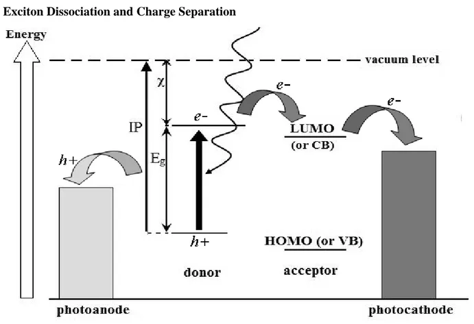
In most polymer semiconductors, excitons have a binding energy of a fraction of an eV and it is necessary to incorporate materials with a suitable offset in the energy levels within the photoactive layer to dissociate these excited states. In nanoparticle–polymer PV cells the nanoparticles have a relatively low electron affinity and accept electrons from the polymer under illumination. The electrons are accepted by the LUMO (in the case of organic nanoparticles) or the conduction band (in the case of inorganic nanoparticles) (Figure 1.5). The polymer acts as an electron donor. This process results in exciton dissociation.
Maximization of the exciton dissociation at the junction of the donor and acceptor phases leads to the concept of the bulk-heterojunction. Blending conjugated polymers with electron acceptors, such as fullerenes, is a very efficient way to break apart photogenerated excitons into free charge carriers. Ultrafast photophysical studies showed that the photoinduced charge transfer in such blends happens on a time scale of 45 femtoseconds. This is much faster than other competing relaxation processes (photoluminescence usually requires around 1 ns).94
During the excitons diffusion, excitons may end their existence via disadvantageous decay channels by recombination. Two different recombination mechanisms have to be taken into account: germinate recombination and bimolecular (Langevin) recombination. Germinate recombination describes the process where an interfacial polaron pair is created but the charge carriers cannot overcome the coulombic attraction and recombine radiatively or non-radiatively, whereas bimolecular recombination occurs if an electron and a hole from two different excitons recombine as they are not transported to the electrodes quickly enough. Thus, bimolecular recombination is sometimes also referred to as a second order recombination.
iii) Charge Transport
Once the charge separated state is formed, the free charges must be allowed to reach the electrodes where they constitute the photocurrent from the device. High charge carrier mobilities significantly increase the charge transport efficiency as fast extraction of charges reduces the probability for recombination. Slow extraction may cause permanent or temporary trapping of charges into localized states. As the risk for trapping increases with the distance travelled, a thin layer is always beneficial for the device efficiency. If charge carrier mobilities are unbalanced, local accumulation of charge density may become sufficiently high in the device to modify the electric field distribution. This phenomenon leads to a nonlinear increase of the photocurrent with linearly increasing light intensity.
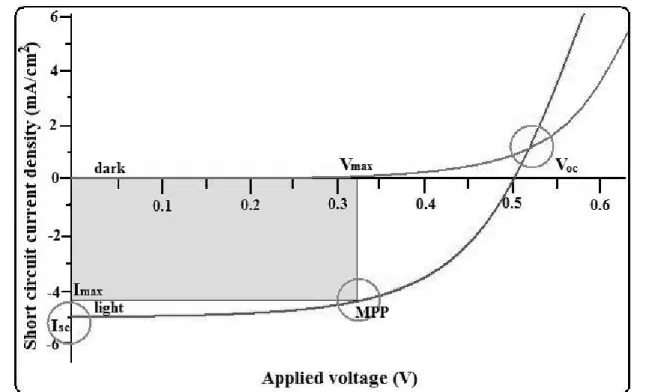
Figure 1.6 I
−
V characteristic of a solar cell showing the relevant parameters, i.e., the open-circuit voltage (VOC), the short-circuit current (ISC) and the square ImaxVmax used to calculate the PCEOn the basis of these three steps described above the overall PCE can be calculated from some key parameters. Among them, the following are very important to describe the performance of a solar cell and its characteristics. They are: short-circuit current (Isc); open-circuit voltage (Voc); fill factor (FF); maximum power point (MPP). These parameters can be obtained from a combined plot, the current−voltage (I−V) curve, under illumination as shown in figure 1.6.
The Isc denotes the current flow per unit area when no external voltage is applied under illumination. Charge carriers generated by illumination are free to drift towards the appropriate electrodes: electrons towards the cathode and holes towards the anode. The result is a photogenerated current which is dependent upon the rate of exciton formation, charge separation, recombination and charge mobility. The Voc describes the effective potential gap in the device. In order to measure this value, a potential difference is applied to the cell and varied until the current drops to zero. The Voc is the maximum expected voltage output under operating conditions, and is directly related to the band gap of any hole or electron transport assist layers and limited by the electrodes, as the band gap of the active layer (Voc, theoretical) is greater than that of the electrodes (Voc, Max). In order to create highly efficient solar cells, both, Isc and Voc should be as large as possible.
The PCE, that is the ratio of the maximum power output (Pmax) to incident light power (φc), can be derived from I−V curve based on the figure 1.6.
________________________________________________________________________________________________
15
PCE = Pmax/φc ---(1)
As the solar cell generates power, a certain amount of current density is passing through the device even though no voltage is applied. This is the short circuit current density (Isc), corresponding to the Isc normalized to the active area. To stop the current flow, a certain voltage (Voc) has to be applied. As the output power density of the solar cell corresponds to the product of voltage and current density, the maximal power will be generated somewhere around the maximum power point (MPP). The ratio between the power density at the MPP and the product of Voc and Jsc is called the fill factor. From this, it is possible to calculate the PCE of the device with respect to the incident light power density Pin, and FF
PCE =Voc Isc FF/Pin ---(2)
The fill factor which describes the shape of the I
−
V curve is defined as the ratio between the MPP (gray area in the curve) and the product of shortcircuit current density and open-circuit voltage (Figure 1.6).FF =MPP/Voc Isc --- (3)
Another important parameter is external quantum efficiency (EQE). The EQE is the ratio of the number of photo-generated electrons collected under short-circuits conditions to the number of incident photons. The PCE for a cell generally increases with the EQE but a high EQE value does not necessarily guarantee a high PCE.
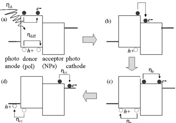
Figure 1.7 Illustration of the consecutive processes leading to a photocurrent within nanoparticle–
polymer PVs
The process of charge generation and transport within OPV cells is believed to occur in five consecutive steps (Figure 1.7). Each step is characterized by a specific efficiency and the product of all singular efficiencies determines the EQE.95
EQE = ηA ηdiff ηdiss ηtr ηcc ---(3)
In Eq. (3) ηA is the photon absorption yield. This is determined by the optical absorption coefficient of the photoactive layer and its thickness. The parameter ηdiff is the exciton diffusion yield, which represents the ability of exciton to diffuse through the polymer without recombination (Figure 1.7 a). If the average diffusion length that the exciton must travel to reach a heterojunction is relatively large compared to Lex (exciton diffusion length) then recombination of the charge carriers is favored and ηdiff <1. The parameter ηdiss is the exciton dissociation yield which is the probability that the hole and electron will be separated by the internal electric field at a heterojunction (Figure 1.7 b). The energy required to separate the exciton96 is ca. 0.4 eV in a polymer semiconductor. In a well-designed nanoparticle–polymer cell the energy required to separate the exciton is provided by the energy difference (offset) between the LUMOs of the donor and acceptor (Figure 1.7).
The parameter ηtr is the charge carrier transport yield (Figure 1.7 c). Charge transport involves hopping processes and is affected by traps in the composite film. Traps originate from structural
________________________________________________________________________________________________
17
defects or impurity species. They provide localised energy minima of variable depth for charge transport which reduce charge mobility.
The collection of charge at the electrodes is also crucial to overall efficiency (Figure 1.7 d). The parameter ηcc is the charge collection yield. This parameter represents the ability of the charges to be transferred from the photoactive layer to the electrodes. It is a function of the energy levels of the components (Figure 1.7) and the interfacial contacts between the photoactive layer and the electrodes.97 High ηcc values can occur when (a) the Fermi level of the photoanode is greater than the energy level of the donor’s HOMO and (b) the energy level of the acceptor’s LUMO is greater than the Fermi level of the photocathode (Figure 1.7).
1.3.2 Various Devices and Active Layers
The device architecture plays an important role in organic solar cells. As discussed previously, in organic semiconductors bound excitons are created upon photoexcitation. These excitons have to dissociate for an efficient charge transfer. Since the built-in electric fields are usually not high enough to dissociate the excitons directly, a process has to be introduced that efficiently separates the bound electron−hole pairs. The exciton dissociation is known to occur between two semiconductors such as donor−acceptor interface as well as semiconductor/metal interfaces. The following will give an insight on the most basic types of devices.15
1.3.2.1 Single Layer Devices
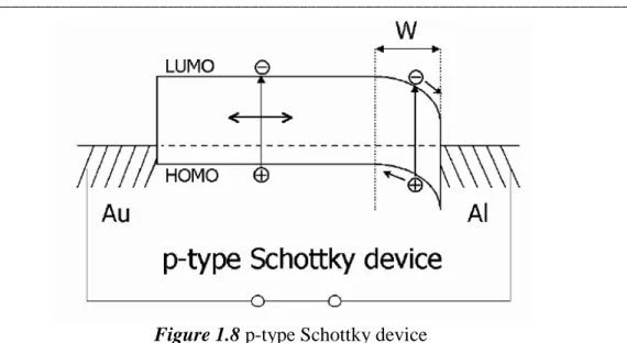
The first organic solar cells were based on a single organic layer sandwiched between two metal electrodes of different workfunction. The rectifying behaviour of these devices can be explained by the formation of a Schottky barrier (for doped semiconducting materials) between the metal with the lower workfunction and the p-type organic layer. Figure 1.8 shows a p-type Schottky device. Close to the contact, the depletion region W, a resulting band bending from the Schottky contact is depicted. This corresponds to an electric field in which the excitons can be dissociated.
Figure 1.8 p-type Schottky device
Therefore, illumination through two different semi-transparent metal contacts can lead to symbatic (proportional to the absorption coefficient) or anti-batic behaviour of the spectral photocurrent.4,98 Since the exciton diffusion length for most organic solar cell materials is below 20 nm, only those excitons generated in a small region within ≤ 20 nm from the contacts contribute to the photocurrent. Owing to high series resistances these materials show a low fill factor and a field dependent charge carrier collection. These thin film devices can work well as photodetectors, since under a high reverse bias the electric field drives the created charges to the electrodes.
1.3.2.2 Bilayer Heterojunction
To overcome the limitation of photoinduced charge carrier generation a bilayer device in which a donor and an acceptor material are sequentially stacked together with a geometrical interface is introduced. At this interface, the charge separation occurs16,99, 100 which is mediated by a large potential drop between donor and acceptor. The bilayer is sandwiched between two electrodes with different workfunctions matching donor HOMO and the acceptor LUMO for efficient extraction of the corresponding charge carriers. For an efficient charge transfer, the LUMO and the HOMO of the donor should lie above those of the acceptor. The bilayer device structure is shown in figure 1.9, neglecting all kinds of possible band bending due to energy level alignments.
While the formation of a classical p/n junction requires doped semiconductors with free charge carriers to form the electric field in the depletion region, the charge transfer in bilayer heterojunction between undoped donor and acceptor materials is due to the differences in the ionization potential and electron affinity of the adjacent materials. Upon photon absorption in the donor D, the electron is excited from the HOMO to the LUMO (S0→S1). If now an acceptor molecule A is in close proximity, the electron may be transferred to the LUMO of A, which is energetically preferential.
________________________________________________________________________________________________
19 ID*−AA−UC<0
where ID* is the ionization potential of the excited state (D*) of the donor, AA the electron affinity of the acceptor and Uc the effective coulombic interaction, respectively.
The release in electron energy may be then used to separate the electron and the hole against their coulombic attraction. This photoinduced charge transfer (CT) only occurs under illumination, since it needs the excitation energy of the electron in the donor to reach the LUMO in the acceptor.
There are experimental indications101,102,103 supported by theoretical considerations104 of a formation of an interfacial dipole between the donor and acceptor phases, independent of illumination. This can stabilize the charge separated state by a repulsive interaction between the interface and the free charges. Therefore, the success of the donor/acceptor concept lies to a great extent in the relative stability of the charge separated state: the recombination rate between holes in donor and electrons in the acceptor is several orders of magnitude smaller than the forward charge transfer rate.105
After the excitons are dissociated at the interface the electrons can travel within the n-type acceptor and the holes within the p-type donor material. Hence, holes and electrons become effectively separated from each other and collected by the cathode and anode, respectively. As a consequence, the photocurrent dependency on illumination intensity can be linear.106
1.3.2.3 Bulk Heterojunction
The essence of bulk heterojunction is to blend the donor and acceptor components in a bulk volume so that each donor−acceptor interface is within a distance less than the Lex (ca. 10 nm) of each absorbing site.
The dispersion of semiconducting nanoparticles within the polymer phase to give bulk (or dispersed) heterojunction (BHJ) cells (Figure 1.10). These PV cells may result in a much greater PCE with respect to that achievable with anyone of the previously described architecture due to;
a) the decreased distance the excitons must diffuse to reach the interface (the average polymer phase domain size (Lpol) being lower than Lex,
b) the much greater area of the acceptor/donor interface.
Figure 1.10 Bulk heterojunction configuration in organic solar cells. 1.3.2.4 Diffuse Bilayer Heterojunction
Another device architecture, which is conceptually in between the bilayer and the bulk heterojunction device is a diffuse bilayer heterojunction device, combining the advantages of both concepts, that is an enlarged donor/acceptor interface and a spatially uninterrupted pathway for the opposite charge carriers to their corresponding electrode. The diffuse interface is achieved in different ways: if processed from solution, two thin films can be pressed together in a lamination procedure applying moderate pressure and elevated temperatures.3 Another way to achieve a diffuse
________________________________________________________________________________________________
21
interface is to spin cast the second layer from a solvent that partially dissolves the underlying layer.107 , 108 Finally, also the controlled interdiffusion between an acceptor molecule such as a fullerene derivatives and donor polymer by annealing of a bilayer device109 results in an intermixed interfacial region.
The earlier polymer cells contained a heterojunction bilayer, i.e., the donor and acceptor phases were deposited sequentially on top of each other and had a single common interface (Figure 1.11a). Because almost all of the excitons were generated at a distance more than Lex away from the heterojunction interface very low PCE values were found because ηdiff <1. This problem was addressed by dispersing semiconducting nanoparticles within the polymer phase to give bulk (or dispersed) heterojunction (BHJ) cells (Figure 1.11b). These PV cells have much greater PCEs due to (a) the decreased distance the excitons must diffuse to reach the interface, i.e., the average polymer phase domain size (Lpol) is less than Lex and (b) the much greater area of the acceptor/donor interface. The BHJ is a space-filling aggregated dispersion of nanoparticles or other hetrogenious nanodomains within a solid polymer phase. In colloid terms, the BHJ is a bicontinuous solid dispersion where both the nanoparticle and polymer phases are semiconducting. The morphology of the ideal nanoparticle–polymer photoactive layer is similar to that present within bicontinuous microemulsions. This may be thought of as an interpenetrating nanoparticle network whose connected nanoparticle segments are separated by a curved polymer phase.
Figure 1.11(a, b) Bilayer and bulk hetrojuncation layer diffrence
1.4 Hybrid Solar Cell Concepts
Hybrid solar cells are a mixture of nanostructures comprising both organic and inorganic materials. Therefore, they combine the unique properties of inorganic semiconductor nanoparticles with the properties of organic/polymeric materials.110 In addition to this, low cost synthesis, processability and versatile manufacturing of thin film devices make them attractive.14, 111 Also, inorganic semiconductor nanoparticles may have high absorption coefficients and particle size
Lex
induced tunability of the optical band-gap. Thus, the organic/inorganic hybrid concept for PV cells is becoming more and more interesting and attractive in the recent years.
In the literature, hybrid solar cells are manufactured using different concepts such as solid state DSSCs,112,113,114 and hybrid solar cells using the bulk heterojunction concept with different nanoparticles such as TiOx, 115 ZnO, 116 CdSe, 117,118 CdS, 11 PbS, 119 and CuInS2. 120, 121
1.4.1 Solid state dye-sensitized solar cells (DSSC)
In a solid state DSSCs the electrolyte is replaced with a p-type semiconductor or organic hole conductor materials122,123,124 avoiding problems such as leakage of liquid electrolytes.125
A solid state DSSCs is schematically shown in figure 1.12. The mesoporous metal oxide electrode, commonly, TiO2 is placed in contact with a solid state hole conductor. Attached to the surface of the nanocrystalline electrode film is a monolayer of the sensitizing dye. After the excitation of the dye an electron is injected into the conduction band of the semiconductor oxide electrode. The sensitizer dye is regenerated by the electron donation from the hole conductor.126 In the solid state cell, the charge transport is electronic whereas on using liquid or polymer electrolyte, ionic transportation takes place.127
Figure 1.12 Solid state dye-sensitized solar cell
The hole conductor must be able to transfer holes from the sensitizing dye after the dye has injected electrons into the TiO2; i.e., the upper edge of the valence band of p-type semiconductors must be located above the ground state level of the dye (Figure 1.13).
________________________________________________________________________________________________
23
Figure 1.13 Energy diagram for an efficient charge transfer between solid state DSSC components
Furthermore, hole conductors have to be deposited within the porous nanocrystalline layer penetrating into the pores of the nanoparticle and finally it must be transparent in the visible spectrum, or, if it absorbs light, it must be as efficient as the dye in the electron injection. CuI, CuBr or CuSCN were found to be the successful candidates to replace the liquid electrolyte,128 ,129 although the achieved energy conversion efficiency (solid state solar cell of nanoporous n-TiO2/cyanidin/p-CuI) was only 1%.130 The efficiency was improved to 6% by Tennakone et al.,122 with a n.TiO2/ruthenium bipyridyl/CuI cell, the interface of TiO2/CuI degrades due to the release of iodine and the formation of a trace amount of Cu2O and/or CuO.131 A better stability was observed by covering the TiO2 electrode with a thin MgO layer.132 , 133 Kumara et al. used 1-methyl-3-ethylimidazoliumthiocyanate (MEISCN) which is a molten salt, resulting in a PCE of 3.75% and a peak IPCE of 59%.134 CuSCN is an alternative to replace CuI with a more stable performance. Again, the obtained efficiency was always below 2%.128,135
Bach et al.124 reported a dye-sensitized heterojunction between TiO2 with the amorphous p-type semiconductor 2,2′,7,7′-tetrakis(N,N-di-p-methoxyphenyl-amine) 9,9′-spirobifluorene (OMETAD) as an organic hole transport material. By blending the hole conductor matrix of spiro−OMETAD with a combination of 4-tert-butylpyridine (t−BP) and Li[CF3SO2]2N, Kruger et al.136 reported an efficiency of 2.56 %, by performing the dye adsorption in the presence of silver ions in the dye solution.137 Mende and Gratzel138 demonstrated 4% efficiency and also showed that
if the pores of nanoporous TiO2 are not completely filled this leads to lower current densities and poorer performance of the cell under sunlight.
Conjugated polymers have also found application in DSSCs139 However, high molecular weight polymers solution-cast do not penetrate into the pores of the nanoparticles.140 A polymeric gel electrolyte is considered as a compromise between liquid electrolytes and hole conductors in quasi solid state DSSCs.141 Polymer electrolytes are composed of alkaline salts dissolved in a high molecular mass polyether host or polypropylene oxide host.140 In polymer electrolytes, the polymer matrix should be an efficient solvent for the salt, capable of dissociating it and minimizing the formation of ion pairs. poly(3 alkylthiophenes) were used to replace the liquid electrolyte by Sicot et al.142 and Gebeyehu et al.113. A mixture of NaI, ethylene carbonate, propylene carbonate and polyacrylonitrile was studied by Cao et al.143 Poly (vinylidenefluoride- co-hexafluoropropylene) (PVDF-HFP) used to solidify 3-methoxypropionitrile (MPN) was utilized by Wang et al.144 with conversion efficiencies under full sunlight of over 6%, showing high stability under thermal stress at 80 °C as well as under prolonged soaking with light.
Nogueira et al. reported solid state DSSCs by employing a copolymer, poly(epichlorohydrin-co-ethylene oxide), Epichlomer-16 as electrolyte with PCEs up to 2.6%.145 Haque et al. reported flexible solid state dye-sensitized solar cells using Al2O3 coated TiO2 electrodes and an I2 /NaI-doped solid state Epichlomer-16 electrolyte with an efficiency of 5.3%.146 Kaneko and Hoshi reported efficiency of 7% with a solid state DSSC incorporating polysaccharide involving redox electrolytes.147
1.4.2 Nanoparticle sensitized TiOx solar cells
Hybrid solar cells can be prepared by replacing the dye with inorganic nanoparticles or quantum dots. They can be adsorbed from a colloidal QD dispersion148 or produced in-situ.149 Inorganic nanocrystals used instead of organic dyes may allow tunability of the band-gap and thereby of the absorption range. Nanocrystals are relatively stable inorganic materials have large extinction coefficients due to quantum confinement and intrinsic dipole moments. Their sharp interface may promote rapid charge separation. To embed the particles into porous TiO2 films and to use those modified layers as light converting electrodes,150 the incorporated nanoparticles need to be much smaller than the pore sizes of the nanoporous TiO2 electrodes.
________________________________________________________________________________________________
25
1.4.3 Extremely thin absorber (ETA) solar cells
Extremely thin absorber (ETA) solar cells are conceptually close to the solid state DSSCs. 151
In the ETA solar cells, an extremely thin layer of a semiconductor such as CuInS2 or CdTe or CuSCN replaces the dye in TiO2 based solar cells.152 The ETA solar cell has the advantage of enhanced light harvesting due to the surface enlargement and multiple scattering. Similar to the solid state DSSCs, the operation of the ETA solar cell is also based on a heterojunction with an extremely large interface. Nanu et al.153 fabricated TiO2/CuInS2 ETA solar cell using atomic layer chemical vapour deposition technique. A 2 nm Al2O3 tunnel barrier and a 10 nm thick In2S3 buffer layer were inserted between TiO2 and CuInS2 to overcome the interfacial recombination problem. This kind of cell gave an energy conversion efficiency of 4%.
1.4.4 Hybrid Solar Cells Based on Bulk Heterojunction Concept
An effective strategy for hybrid solar cell fabrication is to use blends of nanocrystals with a semiconducting polymer as a photovoltaic layer. The BHJ concept for OPV cells has been described previously.154,155,156, 11 The same general concepts apply in hybrid solar cells is similar to that used in organic solar cells. Excitons created upon photoexcitation must split as free charge carriers at interfaces between two semiconductors in a composite thin film such as a conjugated polymer and fullerene mixture.9 Exciton dissociation is known to occur very efficiently at interfaces in such a composite.
Greenham et al. studied the first hybrid systems containing CdS or CdSe nanoparticles embedded in MEH-PPV. As an aggregation-preventing ligand for the nanoparticles, the surfactant TOPO was used. This surfactant, however, rather hinders charge transport between the nanoparticles and charge transfer from the conjugated polymer onto them. Further, an extension to the polymer absorption band could be achieved due to the added absorption of the nanocrystals. To reach relatively high PV performances, the system required a high load (> 80%) of nanocrystals to be incorporated, similar to the MEH-PPV:PCBM system.86 Applying pyridine as a replacement for the TOPO layer, the first hybrid p−n type PV devices were presented.
Figure 1.14 Hybrid polymer solar cells prepared by blending CdSe QDs with rr−P3HT
A major step in the development of hybrid polymer solar cells was achieved by blending CdSe nanoparticles with regioregular P3HT (Figure 1.14). In 2002, Huynh et al. reported AM 1.5 PCE of 1.7% and EQEs reaching 54% with that system.118 In this study the aspect ratio of the CdSe nanocrystals was varied roughly between 1 and 10, and the authors reported the best photovoltaic efficiencies for nanorods having the most elongated structure (7 by 60 nm). The authors concluded that the elongated nanorod-like nanocrystals provide a better charge transport through band transport than shorter ones, where many hopping processes between the nanoparticles limit charge transport.
In a related study, Huynh et al. demonstrated control of the P3HT:CdSe nanorod blend morphology in thin films by applying a solvent mixture of chloroformand pyridine.157 A pyridine concentration of about 8% yielded the finest intermixing of P3HT and CdSe nanorods, which was reflected by smooth film topographies. A thermal annealing step was applied at reduced pressure to remove excess pyridine from the blend, and consequently improve the EQE. Pientka et al. studied photoinduced charge transfer from CdSe and InP nanocrystals onto MDMO-PPV.158 , 159 The authors confirmed the use of pyridine to be favourable for efficient charge transfer as compared to more extended octylphosphine-containing organic ligands around the nanoparticles. These results were obtained by using photoluminescence quenching, photoinduced charge transfer and light-induced spin resonance measurements.
________________________________________________________________________________________________
27
1.5 Role of Carbon Nanotube in Solar Cells
Carbon nanotubes (CNTs) were first discovered by Iijima in 1991. They are essentially graphene sheets rolled into the form of a tube, loading to either SWNT or multi-walled nanotubes (MWNT) (Figure 1.15). CNTs have attracted considerable attention due to their unique electrical, mechanical, optical and chemical properties.160 These excellent properties make carbon nanotubes promising materials for numerous applications.
Figure 1.15 Single-walled nanotubes (SWNT) and multi-walled nanotubes (MWNT)
SWNTs can be semiconducting or metallic, depanding on the type of chiralitiy (the arrangement of the carbon honeycomb with respect to its axis). Semiconducting CNTs have generally been found to be p-type with a high predicted mobility.161 Like C60, CNTs have been introduced into conjugated polymers to produce organic photovoltaic devices.162 Well-spaced and symmetric structures exist in the local density of states of SWNTs due to their one D nature of the conduction electron states. All of the bands have a direct band gap, which is inversely proportional to the tube diameter. The fundamental energy gap is zero in the metallic SWNT nanotubes and on the order of about 0.5 eV in semiconducting ones. By combining SWNTs of different diameters and chiralities, and correspondingly/different band gaps, it is possible to obtain a continuous response over a broad spectral range. Some of the characteristics feature of, CNT are the following: density (g/cm3) 0.8–1.2, band gap (eV, 300K) 0.3–2.0, resistivity ( Ω cm, 300K) 0.1, electron mobility (cm2/ Vs, 300K) 108, hole mobility (cm2/V s, 300K) 103.163
Table 1.3
Performance of typical carbon-based photovoltaic cells164
Material Jsc (mA/cm2) Voc (V) FF η (%)
CNTs/n-Si 26 0.54 0.53 7.4
P3HT/C60-CNTs 2.7 0.54 0.49 0.75
CNTs-P3OT/n-Si 2.9 0.22 0.27 0.175
MWNTs/PEDOT-PSS (DSSC) 15.5 0.66 0.63 6.5
Graphene/PEDOT-PSS (DSSC) 13.0 0.72 0.48 4.5
Due to their electronic properties, CNTs have been considered as possible components of hybrid BHJ-type systems. Free electron/ hole pairs excited by photons can be either separated by an externally applied voltage,165 by internal fields at the Schottky barriers,4 at p–n junctions or at defects and a photocurrent can be generated166 The photocurrent in CNT junctions is thought to involve band-to-band transitions and photon-assisted tunneling based on the observed multiple sharp peaks in the infrared, visible and ultraviolet. Besides individual CNT, CNT macro-bundles and films also produce a photocurrent.
Back electrode (that is, the electrode not hit directly by the light) made from CNTs is yet another important application in solar cells. Thin, transparent layers comprising bulk metallic SWNTs have been proposed as efficient system for providing lateral electrical conductivity collecting current from the front surface of thin-film solar cells. The thickness of the CNT films must be chosen so that the layer should contribute significant lateral electrical conductivity, yet would be as nearly transparent as possible to incident light. CNT coatings and circuits are becoming one of the latest alternatives to traditional conductive materials, e.g. ITO, fluorine-doped tin oxide (FTO), zincoxideorcadmiumsulfide. Several groups have reported on performance of CNTs based photovoltaic devices (Table 1.3). The cell may shows efficiency up to = 7.4% at AM 1.5 (100 mW/cm2) with a VOC of 0.54 V and a short-circuit current density (JSC) of 26 mA/cm2. These results represent a first step toward further realizing carbon-based solar cells.164
Recently, to give CNTs more opportunities for new applications in various areas, many methods were used to modify their surface, such as grafting with polymers,167 organic molecules, inorganic molecules and biological molecules.168 The resulting modifiedand CNTs are often suitable for the fabrication of CNTs-based nanocomposites. Combinations of CNTs with different inorganic nanoparticles were investigated by many researchers. Magnetic nanoparticles,169 TiO2 coated, 170 gold nanoparticles171 and QDs,such as CdTe, CdSe and CdS, 172 have been combined
________________________________________________________________________________________________
29
with CNTs and proposed or investigated as components in electronic, magnetic and catalytic applications, or used as sensitive nanotube molecular sensors and photoactive layers.172
To date, several strategies have been developed to prepare these CNT/nanoparticle composites, including hydrogen bonding,172 (a) in-situ growth, 171, 172 (a,b) covalent linkage 172 (c,d,e) and electrostatic interaction. 172 (g) However, each strategies have been presents still some limitations. For example, in the covalent linkage and in-situ growth approaches, the atomic lattice and electronic properties of CNTs and nanoparticles are likely to undergo significant changes. As an example, the hybrid nanostructures have not shown the fluorescent labelling behaviour typical of these nanoparticles.172 (i) There have been some reports about attaching nanoparticles to CNTs by electrostatic interaction using ATRP polymerization of polyacrylonitrile at the CNT surface. 172 (h) However, CNTs could not be stably dispersed in the surfactants probably due to their higher specific gravity and entanglements. Therefore, to achieve such nanohybrids with good dispersibility and inherent properties of functional nanoparticles remains a challenge, despite the efforts of pioneering works.
Surface modification of CNTs is often intended to enhance their compatibility (e.g. with a polymer matrix) and dispersibility properties.173 The noncovalent functionalization of CNTs include noncovalent surface coating with surfactants,174 surface wrapping with long polymer chains such as polystyrene sulfonate and hydrolyzed poly(styrene-alt-maleic anhydride),175 noncovalent adsorption of hydrophilic noncharged polymer chains such as poly(vinylpyrrolidone), 176 poly(vinyl alcohol), 177
amylase178 and poly(ethylene oxide),179 on CNTs, and some electron acceptor systems stabilizing CNTs.180 The advantage of noncovalent functionalization is that the structure and original properties of CNTs are not altered after surface modification. However, the surfactants, polymer chains and electric acceptors that can effectively be used for this method are very limited, and high concentrations are usually necessary to obtain dispersions of CNTs, which is inconvenient for further processing carbon nanotubes into composite materials. The dispersions are not very stable and most importantly, it is difficult to further modify CNTs with different functionalities.
1.6 Scope of Work
As described in the introduction part of this thesis: i) the maximum achievable PCEs in PV cells is dependent, among other factors, on the type of materials and the process applied to the active PV layer, ii) CdSe nanocrystals act as electron acceptors when combined with a conjugated polymer and the band gap for such QD can be controlled by adjusting the size of the QDs, iii) the dispersion of QDs in a polymer matrix, however, is efficient to control, while being a critical feature for an efficient charge.
Three different strategies were investigated in this research; all of them aimed at the preparation of a hybrid P3HT/CdSe system in which the different synthetic procedure was aimed at achieving a good dispersion of the QDs in the polymer matrix. The aim of the first scheme is to investigate an approach for the fabrication of active PV materials based on polymer/CNT/nanoparticles nanocomposite by the modifying the CNTs with a grafted polymer suitable for assisting a controlled growth of CdSe nanoparticles onto the CNT polymer surface. In particular, based on the reported effectiveness of polyacrylonitrile as colloidal stabilizer for CdSe nanoparticles the covalent functionalization of CNTs via “grafting from” or “grafting onto” polymerization was performed. Controlled polymerization was expected to favour, in a second step, the localized growth of CdSe at the CNTs surface.
The other two strategies do not include the presence of CNTs. In the second system, a conjugated P3HT-b-PAN block copolymer instead of CNT-g-PAN systems would be considered as the next for growing CdSe nanoparticles. For this purpose, a suitable strategy based on a combination of controlled polymerization procedures followed by “Click” condensation shall be considered and the resulting copolymer exploited for the controlled nucleation and stabilization of CdSe nanocrystals, for which the CdSe surface would be stabilized by coordinating CN groups.
In the third route, P3HT itself was contained acid group at the chain end is reported to promote formation of controlled QDs.
________________________________________________________________________________________________
31
1
C. W. Tang, Applied Physics Letters, 1986, 48, 183. 2
M. Skompska, Synthetic Metls, 2010, 160, 1–15. 3
M. Granström, K. Petritsch, A. C. Arias, A. Lux, M.R. Andersson, R. H. Friend, Nature, 1998, 395, 257.
4
D. Wöhrle, D. Meissner, Advanced Materials, 1991, 3, 129. 5
S. Gu¨nes, H. Neugebauer, N. S. Sariciftci, Chem. Rev., 2007, 107, 1324-1338. 6
G. Yu, A. J. Heeger, Journal of Appied Physics, 1995, 78, 4510. 7
S. A. Jenekhe, S. Yi, Applied Physics Letters, 2000, 77, 2635. 8
A. J. Breeze, A. Salomon, D. S. Ginley, B. A. Gregg, H. Tillmann, H. H. Hoerhold, Applied Physics Letters, 2002, 81, 3085.
9
S. E. Shaheen, C. J. Brabec, N. S. Sariciftci, F. Padinger, T. Fromherz, J. C. Hummelen, Applied Physics Letters, 2001, 78, 841.
10
J. J. Dittmer, E. A. Marseglia, R. H. Friend, Advanced Materials, 2000, 12, 1270. 11
N. C. Greenham, X. Peng, A. P. Alivisatos, Physical Review B, 1996, 54, 17628. 12
Peng, Z. A. and X. Peng, J Am. Chem. Soc.,2001, 123, 183. 13
H. Hoppe, N. S. Sariciftci, D. Meissner, Molecular Crystalls Liquid Crystalls, 2002, 385, 113. 14
N.S. Sariciftci, L. Smilowitz, A.J. Heeger, F. Wudl, Science, 1992, 258, 1474. 15
H. Hoppe, N.S. Sariciftci, J. Mater. Res., 2004, 19(7), 1924. 16
P. Peumans, A. Yakimov, S.R. Forrest, J. Appl. Phys., 2003, 93(7), 3693. 17
C. J. Brabec, F. Padinger, J. C. Hummelen, R. A. J. Janssen, N. S. Sariciftci, Synthetic Metals,
1999,102, 861.
18
S. E. Shaheen, R. Radspinner, N. Peyghambarian, G. E. Jabbour, Appl. Phys. Lett., 2001, 79, 2996.
19
T. Ishikawa, M. Nakamura, K. Fujita and T. Tsutsui, Appl. Phys. Lett., 2004, 84, 2424. 20
(a) B. O’Regan, M. Grätzel, Nature, 1991, 335, 737 (b) M. Grätzel, Nature, 2001, 414, 338. 21
Michael Grätzel, J. Photochemistry and Photobiology C: Photochemistry Reviews, 2003, 4, 145. 22
H. Tomozawa, D. Braun. S. Phillips and A. J. Heeger, Synthetic Metals, 1987, 22, 63. 23
Kim, J. Y., Lee, K.; Coates, N. E., Moses, D., Nguyen, T.-Q., Dante, M., Heeger, A. J., Science,
2007, 317, 222.
24
J. Y. Kim et al., Adv. Mater., 2006, 18, 572. 25
Yang, X., Van Duren, J. K. J., Janssen, R. A. J., Michels, M. A. J., Loos, J. Macromolecules,
![Figure 1.4 Comparison of the solar photon flux with absorption spectra of poly[2-methoxy-5-(3′,7′- poly[2-methoxy-5-(3′,7′-dimethyloctyloxy)-1,4-phenylene vinylene] (MDMO-PPV), poly(3-hexylthiophene) (P3HT), 1-(3-methoxycarbonyl)-propyl-1-phenyl-[6,6]](https://thumb-eu.123doks.com/thumbv2/123dokorg/7551571.109417/11.892.172.729.126.483/comparison-absorption-methoxy-dimethyloctyloxy-phenylene-vinylene-hexylthiophene-methoxycarbonyl.webp)