UNIVERSITÀ DEGLI STUDI DI CATANIA
SCUOLA DI DOTTORATO
Dottorato di Ricerca Internazionale in Ingegneria
dei Sistemi, Energetica, Informatica e delle
Telecomunicazioni - XXIX ciclo
Ph.D. Thesis
Fully Integrated Data and Power Transfer
Systems with Galvanic Isolation
Dott. Ing. PierPaolo Lombardo
Tutor: Prof. Giuseppe Palmisano Coordinator: Prof. P. Arena
Co-tutor: Ing. Egidio Ragonese
STMicroelectronics, Catania
1
Summary
This thesis sums up main activities which I have been carried out at the
Radio-Frequency Advanced Design Center (RF-ADC), a joint research center between STMicroelectronics and the University of Catania, during my three years of Ph.D. studies.
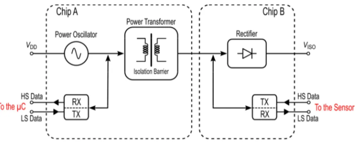
My principal activity was focused on the design of galvanically isolated integrated systems as a part of a research project at the RF-ADC by exploiting STMicroelectronics technology platforms providing on-chip galvanic isolation. This technology was previously addressed to the implementation of isolated data transfer and it is currently used for mass production. In this context, the principal purpose of my work was the investigation on a fully integrated dc-dc power converter with half-duplex data communications providing on-chip galvanic isolation in silicon technologies. This research is mainly interested in increasing the level of integration for the next generation of power converters with data transfer and several other applications requiring galvanic isolation. Autonomous sensors and/or control circuits, typically require a few tens of Mbps for data communication and an output power from tens to hundreds of mW. In this context, fully integrated interfaces can provide several advantages, including higher reliability, lower PCB area, lower system complexity and lower costs, especially if only silicon technology is exploited. The state of the art of isolators concerning data transfer and power devices are presented in Chap. 1.
Integrated dc-dc power converter with on-chip galvanic isolation involves several challenges due to both inherent technology limitations and the highly non-linear interactions between building blocks. It requires customized design
2
strategies to properly adopt the integrated approach. Therefore, this thesis focuses on fully integrated systems, with the aim of filling this gap by implementing both data and power transfer in silicon technology. This is a complex task that requires accurate evaluation of on-chip and off-chip parasitics, modelling of integrated passive devices, and customized active and passive circuit co-design. In particular, my principal design activities was focused on both dc-dc isolated power converters at different output power levels and data/power transfer systems for autonomous sensors. They are the object of Chapter 2, Appendix A and Chapter 3, respectively. These systems have been integrated in the aforementioned technology and successfully characterized. To the best of the author’s knowledge, this is also the first reported system of this kind which do not require post-processing steps, therefore demonstrating the feasibility of power with/without data transfer on silicon technologies and thus promising new and highly-integrated devices to become available.
3
Contents
List of Tables 5 List of Figures 6 SUMMARY ... 1 1. CHAPTER I ... 91.1 Low-power isolated interfaces ... 9
1.2 Applications ... 10
1.3 State-of-the-art of isolators ... 14
1.4 Isolator’s market ... 24
1.5 Aim of this thesis ... 27
1.5.1 Architecture of system ... 28 1.5.2 Technology platform ... 30 1.5.3 Main results ... 31 2. CHAPTER II ... 33 2.1 System description ... 33 2.2 Design issues ... 34
2.3 Efficiency analysis and block design of the isolated dc-dc power converter ... 35
2.3.1 Rectifier ... 37
2.3.2 Oscillator core ... 39
2.3.3 Isolation transformer ... 42
2.4 System design ... 48
4
3. CHAPTER III ... 54
3.1 System description ... 55
3.2 Data modulation ... 58
3.2.1 Pulse-with modulation coding ... 58
3.3 High sensitivity and low power ASK detectors ... 60
3.3.1 Common source ASK detector with adaptive biasing ... 62
3.3.2 HS ASK detector ... 64
3.3.3 LS ASK detector ... 66
3.4 Measurements results ... 68
3.4.1 DC-DC power converter ... 69
3.4.2 Data measurements setup ... 71
3.4.3 High-Speed data communication ... 73
3.4.4 Low-Speed data communication ... 76
4. CHAPTER IV ... 80
5. CONCLUSION ... 87
Power transfer system ... 87
A fully integrated data and power transfer system ... 88
Open issues ... 89
Conclusion ... 89
6. APPENDIX A ... 91
7. APPENDIX B ... 105
5
List of Tables
Table 1.1 Thresholds and limits for continuous 60 Hz current and their effects [8] . 13
Table 1.2 System-level standards involving isolation by market and region [9] .. 14
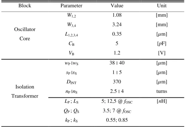
Table 2.1 Simulated rectifier performance, VOUT= 3 V, POUT= 25 mW ... 39
Table 2.2 Design parameters of the power oscillator and the isolation transformer . 52 Table 3.1 Summarized design parameters and simulated performance of the HS ASK detector ... 66
Table 3.2 Summarized design parameters and simulated performance of the LS ASK detector ... 68
Table 6.1 Design parameters of the oscillator and the isolation transformer ... 94
Table 6.2 Isolation transformer geometrical parameters... 97
6
List of Figures
Figure 1.1 Ground loops problem in wireline communication systems [72] ... 11
Figure 1.2 (a) Typical optocoupler structure. (b) X-ray cross section of a device 15 Figure 1.3 Optocoupler equivalent circuit [16] ... 16
Figure 1.4 Typical capacitive isolator system ... 17
Figure 1.5 Photo of the system before packaging [19] ... 18
Figure 1.6 Integrated inductive isolator architecture ... 19
Figure 1.7 (a) Planar isolation transformer. (b) Photo of an inductive isolated system before packaging [21] ... 20
Figure 1.8 (a) Data/power SiP before packaging. (b) Cross-section of isoPower transformer ... 21
Figure 1.9 Simplified IEC 60747-5 and VDE 0884-10 test profiles [30] ... 23
Figure 1.10 Simplified VDE 0884-10 surge test profile [30] ... 24
Figure 1.11 Definition of clearance and creepage [31] ... 24
Figure 1.12 Forecasts for worldwide isolation market [33] ... 25
Figure 1.13 Typical low-power applications requiring isolated data and power transfer... 27
Figure 1.14 Novel architecture for isolated data and power transfer system ... 29
Figure 1.15 Simplified cross-section of the available back end of line with thick 31 Figure 2.1Schematic of the fully integrated data and power transfer system ... 34
Figure 2.2 Power transfer flow diagram ... 36
Figure 2.3 Rectifier efficiency as function of output power for different MNMOS (i.e., M5,6,7,8) ... 38
Figure 2.4 Oscillators topologies for isolated power transfer. (a) Class D Oscillator. (b) Complementary cross-coupled oscillator. (c) Current-reuse oscillator ... 40
Figure 2.5 Isolation transformer schematic ... 42
Figure 2.6 Isolation transformer. (a) Primary windings. (b) Secondary windings. (c) 3D-view ... 43
7
Figure 2.7 Lumped scalable model of the isolation transformer ... 45
Figure 2.8 Error distributions of the geometrically scalable lumped model ... 49
Figure 2.9 Simplified scheme of the design flow ... 50
Figure 3.1 Proposed architecture for isolated data/power transfer system ... 55
Figure 3.2 Simplified schematic of the isolated data/power transfer system ... 56
Figure 3.3 Simulated voltage waveforms of the transformer-coupled oscillator .. 57
Figure 3.4 PWM coding scheme adopted (a). Degradation of the detector’s noise margin due to long sequences of ones or zeroes (b) ... 59
Figure 3.5 Standard architecture of an ASK detector ... 60
Figure 3.6 Passive (a) and common-drain topologies for the envelope detector (b) . 61 Figure 3.7 Typical (ideal) time domain waveform of the modulated signal at the NMOS oscillator VD1/2 (see Fig. 3.2) ... 61
Figure 3.8 (a) Tradition source envelope detector. (b) Novel common-source ASK detector with adaptive biasing ... 63
Figure 3.9 Simplified schematic of the HS ASK detector ... 64
Figure 3.10 Simplified schematic of the LS ASK detector ... 67
Figure 3.11 Micrograph of the overall system assembled on board ... 69
Figure 3.12 Output power, POUT, and power efficiency, η, as a function of the output voltage VOUT @ supply voltage VDD= 3V ... 70
Figure 3.13 Output power, POUT, and power efficiency, η, as a function of the output voltage VOUT @ supply voltage VDD= 3.3V ... 70
Figure 3.14 Simplified description of the BER measurement setup ... 72
Figure 3.15 Simplified flow-chart diagram of the BER measurement system ... 73
Figure 3.16 Measured HS data link waveforms at 2.5 Mbps ... 74
Figure 3.17 Measured HS data link waveforms at nominal bit-rate equal to 20 Mbps ... 75
Figure 3.18 Measured HS data link waveforms at maximum bit-rate equal to 40 Mbps ... 76
Figure 3.19 Measured LS data link waveforms at minimum bit-rate equal to 150 kbps ... 77 Figure 3.20 Measured LS data link waveforms at nominal bit-rate equal to 1 Mbps 78
8
Figure 3.21 Measured LS data link waveforms at maximum bit-rate equal to 3 Mbps ... 79 Figure 4.1 Common-mode feedback approach for CMTI ... 81 Figure 4.2 Multi-resonant approach for CMTI [68]... 82 Figure 4.3 Standard data transfer link adopting the CMT rejection circuit [71] ... 82 Figure 4.4 Frequency response of CMT rejection circuit ... 83 Figure 4.5 Architecture of fully integrated galvanically isolated system providing both data/power transfer on a single isolation transformer while guaranteeing a good CMTI performance... 84 Figure 4.6 System [26] is simulated in presence of ± μ CMTs ... 85 Figure 4.7 The system of Fig. 4.5 is simulated in presence of ± μ CMTs86 Figure 6.1 Simplified diagram block of the isolated dc-dc power converter demonstrated in [43] ... 91 Figure 6.2 Simplified schematic of the fully integrated dc-dc power converter providing a POUT up to 200 mW ... 93
Figure 6.3 Simulated voltage waveforms of the transformer-coupled oscillator .. 95 Figure 6.4 Isolation transformer. (a) Primary winding. (b) Secondary winding (c) 3D-view ... 96 Figure 6.5 Error distributions of the lumped scalable model of the isolation transformer calculated with respect to EM simulations ... 97 Figure 6.6 Isolation transformer (half structure) performance. (a) Primary coil. (b) Secondary coil ... 98 Figure 6.7 Micrograph of the transformer-coupled CMOS oscillator ... 99 Figure 6.8 Micrograph of the full-bridge diode rectifier ... 99 Figure 6.9 Measured output power and efficiency at the transformer secondary winding as a function of load resistance RL (CL = 0, fOSC = 250 MHz) ... 100
Figure 6.10 Measured output power, efficiency, and oscillation frequency at the transformer secondary winding as a function of load capacitance CL with
RL = 130 Ohm ... 101
Figure 6.11 Measured output voltage at the transformer secondary winding ... 102 Figure 6.12 Micrograph of the overall power transfer assembled on board ... 102 Figure 6.13 Measured dc output power and efficiency versus dc output voltage ... 103
9
1.
Chapter I
Introduction
This chapter introduces the object of this dissertation that is a fully integrated half-duplex data and power transfer system with on-chip galvanic isolation. Starting from the state of the art of low-power isolated applications, the aim, the technology platform and the main outcome of this work will be discussed.
1.1
Low-power isolated interfaces
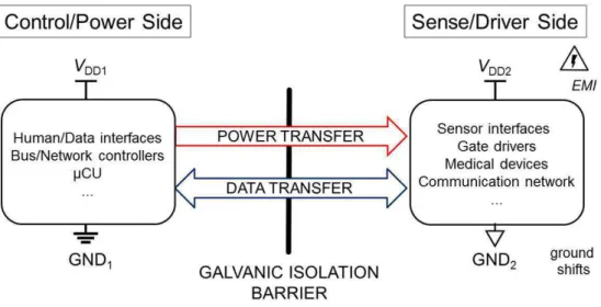
Galvanic isolation is becoming a crucial requisite in the growing field of applications involving measurements and digital control in order to guarantee safety and reliability for both data communication and power supply, especially in harsh operative environments. Indeed, the isolation protects sensitive circuit components and human interface on the control side from dangerous voltage levels present on the sense side, where more robust components such as sensors and actuators reside. Moreover, thanks to the galvanic isolation common-noises or ground loops that affect data acquisition accuracy can be eliminated. To this end, channel isolators with integrated dc-to-dc power converters are typically adopted within on board discrete or system-in-package implementations. Recently significant efforts have been done to improve the level of integration of such isolated systems, thus lowering costs and reducing package and application board sizes. We will briefly present the need for these low-power isolated interfaces in autonomous sensors, and more generally the safety reasons which make isolation mandatory by many system-level standards. Lastly, the state of the art of low-power isolated interfaces will be discussed, along with the relative component-level regulations.
10
1.2
Applications
Wireline Networks
Although RF communication is very popular for consumer applications, when it comes to safety-critical applications wireline networks are the solution of choice. Wireline networks based on TIA-485 standard, commonly known as RS-485, are the most used for transmitting data over long distances in noisy environments with communication distances up to 1.2 km and data-rates up to 10 Mbps [1], [2]. However, the most widespread application of wireline networks are maybe found in the automotive environment: modern high-end vehicles can house up to 120 electronic controller units, indeed, which need to share sensor data or drive actuators. The complexity of in-vehicle communication networks led car manufacturers to define several communication standards, e.g. Local Interconnect Networks, Controller Area Networks (CAN) and Flexray, with the CAN bus as the most successful one, actually gaining popularity even in automation and remote control applications [3],[4]. Both in a large industrial plant or in the small environment of a car, wireline networks are often subject to very high disturbances like electro-magnetic interferences (EMI), voltage surges and ground shifts. A common issue of these networks is avoiding ground loops, as described in Fig. 1.1. Wireline communication requires a low-impedance ground connection between network nodes, which forms a ground loop with the local ground reference of each transceiver. It is unlikely that systems with very far ground references maintain the same potential, and therefore ground potential differences (GDPs) are commonly found in wireline installations. Due to the low-impedance path offered by the ground conductor, even small GPDs can produce high current flowing in the ground loops, which corrupts the signal integrity and can be harmful for both sensitive circuitry and human operators. By providing isolation at the transceiver interface all the systems connected to the bus can be referenced to a single ground, therefore preventing any ground loops. Moreover, any electromagnetic (EM) noise coupled to the cable can cause both GPDs and instantaneous voltage surges in the range of hundreds or even
11
thousands of volts. Typical surges are due to high-current switching loads (e.g. electric motors), or unpredictable events such as electrostatic (ESD) discharges and lightning strikes. These surges can irreparably damage grounded transceiver interfaces, whereas isolation allows the transceiver ground to follow the surge and hence improves the robustness of the network [5]. Low power wireline transceivers for CAN bus and TIA-485 networks operate at 5-V with current consumption around 70 mA in normal operating conditions [6], [7]. Therefore, an isolated power supply providing around 300 mW output power at 5-V is highly desirable to simplify wireline network’s design.
12
Current-monitoring
Recently, applications such as power line monitoring, system protection etc., are required to meet various stringent insulation and safety standards. For example, domestic power line meters measure currents up to 100 A in AC line voltages of 100 VRMS ~ 240 VRMS. Usually, the current is measured at the output of
an isolated sensor such as a current transformer (CT) or a Rogowski coil, or directly across a non-isolated sensor such as a shunt resistor. In the latter case the measurement rides on top of the high voltages and the required isolation is typically gained by using optocouplers connected to the digital outputs. Generally, these systems guarantee a galvanic isolation rating up to 6 kV while providing a CMTI up to 50 ⁄ . However, they often use an external isolating devices μ (CT, Rogowski coil, optcouplers), then a fully integrated system able to transfer both bidirectional data and power with on-chip galvanic isolation represent an ambitious solution showing several advantages in term of costs and complexity. By taking the advantage of this solution the inputs of an ADC can sense the current and transfer the corresponding digital word across the isolation barrier to the low-voltage side while the ADC receiving the isolated power.
Safety reason and system regulations
There are a variety of reasons for requiring galvanic isolation in electrical systems. The most obvious and most critical is the protection of human operators from potentially lethal shocks or the application where a sensor may accidentally encounter high voltage, and the system it is driving must be protect. Shocks hazards can come from the mains power that the equipment is plugged into, or from high voltages generate within an enclosure. The protection of an isolation barrier works in both directions, and may be needed in either, or even in both. For example, when a patients is monitored, the protection in both directions is required: the patient must be protected from accidental electric shock, but if the patient's heart should stop, the ECG machine must be protected from the very high voltages (>7.5 kV) applied to the patient by the defibrillator which will be used to
13
attempt to restart it. As shown in Table 1.1, electrocution due to ventricular fibrillation can be triggered even by relatively low current values. Other mishaps that can represent serious life threats and are directly related to electrical shocks are burns, either directly from sparks or indirectly from increased fire risks, and the involuntary muscle reaction as a consequence of the electric shock.
Table 1.1 Thresholds and limits for continuous 60 Hz current and their effects [8]
Consequently, several safety standard regarding commercial products have been developed to guarantee suitable end-user protection through isolation. They limit voltage and currents which may be in contact with human operators, either in static or transient conditions, and define system specifications, patterns of test-cases, and physical restrictions to be passed by end-products, depending on the applications and for realistic operating conditions. Some examples of commonly used regional and international standards are reported in Table 1.2. Regional regulations are defined by national bodies, such as Verband Deutscher Elektringenieure (VDE), Underwriters Laboratories (UL), and Canadian Standards Association (CSA), for Germany, United States, and Canada, respectively. These agencies also provide system-level testing and certification of products. Their regulations often follow the guidelines of international agencies such as the International Electro technical Commission (IEC) and the European Norms (EN), although there can be substantial differences between each regional version [9].
14
Table 1.2 System-level standards involving isolation by market and region [9]
The main concept behind these regulations is that three levels of protection are commonly defined, that are basic, double, and reinforced insulation [10]. Basic insulation is ascribed to a system which provides isolation while protecting the end user from potentially lethal shocks, as long as the isolation barrier is intact. Double insulation is often mandatory for end-user products. It requires a second insulation system to guarantee basic protection even if the first insulation system fails, thus providing redundant protection. The simple way to obtain double insulation is by cascading two basic-insulation systems, thus increasing costs and complexity and limiting the performance of the system. As a result, reinforced insulation has been introduced, and it is the most used isolation level, being defined as a single insulation system which guarantees electrical-shock protection equivalent to double insulation. For a given application, system designers must choose the insulation characteristics of each component to meet system-level standards.
1.3
State-of-the-art of isolators
Optocouplers and discrete transformers have traditionally been used to guarantee isolation for data transfer and their low-power supplies. Recently, research efforts have been addressed towards the development of reliable and low-cost integrated implementation able to replace these traditional approaches. Typically, data transfer with galvanic isolation have been achieved by using RF links [11], capacitive coupling [12] or integrated coreless transformers [13], [14]. These devices are commonly referred to as “digital isolators” or simply “isolators”. As far as power transfer is concerned, discrete transformers are still the solution of choice even for the aforementioned
15
low-power applications (<<1W). However, data and power currently exploit different channels to be transferred through an isolation barrier, thus increasing size area and costs.
Optocouplers
Optocouplers exploit the light to transfer electrical signals, normally in the near-infrared region. The typical internal structure of an optocoupler is described in Fig. 1.2(a), while an x-ray scan of a device is shown in Fig. 1.2 (b). Two separate metal frames include a light source and a photodetector, respectively. A GaAs light emitting diode (LED) and a phototransistor are commonly used to generate and detect the light. The dice are coated with the molding compound which provides isolation from external light, galvanic isolation, and the mechanical substrate for the metal frames. The spacing between the two dice depends on the isolation rating of the device, being typically greater than 400-μm for high-end products. The highest isolation and speed performance is achieved including more than one dielectric material within the package, for example silicon lens can be used to increase isolation and sensitivity of the photodetector [15], but they also increase costs and complexity of the package.
16
Optocouplers have been historically used to implement both analog and digital data-transfer links since they exhibit several cost and size advantages over the only alternative available in the past, i.e. bulky discrete pulse-transformer. However, they are rarely used because they are slow, power hungry, difficult to integrate with other function, and due to intrinsic time variability of their performance. Fig. 1.3 shows the common equivalent circuit of an optocoupler.
Figure 1.3 Optocoupler equivalent circuit [16]
It is characterised by the current transfer ratio (CTR) that is the ratio of the output current of the phototransistor IOUT versus the input current of the LED IIN.
Biasing currents define the bandwidth of the link and hence are proportional to the data rate. State-of-the-art high-speed optocouplers draw more than 30 mA for a 40-Mbps link. Being related to the phototransistor current gain β, the CTR depends on both biasing currents and temperature and changes widely between each sample. These dependencies are accentuated by the great temperature sensitivity of GaAs and the impact of aging on the LED brightness. This last aspect is particularly important since the LED aging is accelerated with higher current levels, therefore a trade-off exists between performance and lifetime of the device [16].
17
Capacitive isolators
Capacitive isolators rely upon high-voltage capacitors able to sustain the required voltage while providing galvanic isolation. Although advanced or exotic technologies have been proposed [17], [18], the most diffused and integrated approach adopt the inter-metal dielectric (IMD) commonly used in silicon manufacturing technology, that is silicon di-oxide (SiO2), to achieve isolation.
Fig. 1.4 shows a typical single-channel capacitive isolator system. Internally isolator consist of two chips: a transmitter and a receiver. The actual isolation barrier is provided through the high-voltage capacitors located on the receiver chip. The right diagram in Fig. 1.4 shows the cross section of a high-voltage capacitor. Bond wires leaving the transmitter chip attach to the aluminium top plate of the capacitor on the receiver side. The bottom plate, also aluminium, connects to the receiver logic. Between the plates is the interleaved dielectric, a 16-μm thick level of silicon dioxide (SiO2). The transmitter adopts
radio-frequency (RF) amplitude modulation, usually on-off keying (OOK), to transfer the data across the insulation barrier. The receiver performs filtering of the input signal to reject interferers and common-mode disturbances, and amplitude demodulation to recover base-band data. By working at very high frequency (VHF), this approach enables low values for the isolation capacitors and simplifies the filtering.
Figure 1.4 Typical capacitive isolator system
The benefits of using SiO2 as inter-level dielectric are twofold. First, it is
18
therefore, extends the life time expectancy of capacitive isolators well beyond those of competing technologies. Second, SiO2 can be processed using standard
semiconductor manufacturing, thus contributing to significant lower production costs. Fig. 1.5 depicts a micrograph of the isolator before packaging [19]. Moreover, capacitive isolators offer higher level of integration than optocouplers and their high impedance entails very low current consumption.
Figure 1.5 Photo of the system before packaging [19]
Clearly, the fully integrated insulation approach is the key factor in providing these advantages: silicon di-oxide is known as one of the best dielectric insulator with reported dc dielectric strength around 850 μ⁄ for pure samples, which is much higher than organic-based compounds [20].
Unfortunately, capacitive isolators suffer by high sensitivity to common-mode transients (CMTs) and electric fields. Indeed, the two isolated interfaces having two different grounds can be affected by grounds shift that cause common-mode currents to flow through isolation capacitors causing hazardous voltages and/or data corruption. A key parameters of isolators is their ability to reject fast common-mode transients, commonly indicated by common-mode rejection (CMR) or the common-mode transient immunity (CMTI) measured in kV/µs. It is measured by applying sharp voltage pulses between the two isolated ground references of the device, and defined as the maximum voltage slew-rate that the isolator is able to withstand without affecting its data transfer
19
performance. Typical values for CMTI are lower than 25 kV/µs for optocouplers, whereas capacitive isolators can achieve CMTI up to 100 kV/µs thanks to differential signalling even if a complex additional circuitry is required.
Magnetic Isolators
Magnetic isolators, and particular the inductive ones1 exploit a changing magnetic field between two coils to communicate across an isolation barrier and they are the most diffused integrated approach in semiconductors manufactures. As in a capacitive isolators, two chips include a transmitter and a receiver, whereas the dielectric of the planar transformer is exploited to guarantee galvanic isolation, as depicted in Fig. 1.6. In 2001 Analog Devices introduced the first magnetic isolator with the iCoupler technology [21]. The planar transformer has been fabricated by using two stacked spiral coils which are isolated by a thin-film dielectric, as shown in Fig. 1.7 (a). The iCoupler technology adopts a 20-25 µm-thick polyimide (PI) layer to perform isolation, depending on the isolation rating.
Figure 1.6 Integrated inductive isolator architecture
1
Other magnetic isolation techniques include Hall-effect and giant magneto resistance links, which can be only used for data transfer applications. Besides, isolation in these technique is often achieved at the package level, similarly to optocouplers.
20
A 6-μm thick electroplated Au layer is used for the top transformer spiral, whereas the IC top metal layer is used for the bottom one. A photo of a four-channel isolator before packaging is shown in Fig. 1.7 (b). Differently from capacitor-based isolators, transformer-based isolators are more suited for data and power transfer. Indeed, the capacitive coupling between transformer’s windings is a parasitic effect, which is further reduced when high dielectric thickness is used, thus increasing both CMTI and isolation rating. Several systems able to transfer both data and power in packages (SiPs) are currently available in the aforementioned technology, with output power levels from tens to few hundreds of milliwatts and data transfer channels in a multi-die SiP, depending on the output power and complexity of the device [22].
Figure 1.7 (a) Planar isolation transformer. (b) Photo of an inductive isolated system before packaging [21]
The micrograph of one of these systems is shown in Fig. 1.8 (a). It is worth nothing that the data and the power transfer exploit different channel, thus requiring different transformer. Moreover, for power transfer applications both power transformer’s coils require thick Au metals to achieve good efficiencies, thus increasing manufacturing costs. Recently, a lot of products exploiting on-chip galvanic isolation have become available for the application discussed in Section 1.2, e.g. general purpose isolators [23], [24], [25], fully integrated isolated
21
data and power transfer [26], isolated analog-to-digital converters [27], digital isolators [28] and so on.
Figure 1.8 (a) Data/power SiP before packaging. (b) Cross-section of isoPower transformer
To enable cost-effect integration, the main challenge of the isolated dc-dc power converter with data transfer is achieving a good trade-off between efficiency and power density while providing a high data rate with a good CMTI performance.
Component regulations
Component regulations are the counterpart of system regulations defining the components specifications needed to guarantee a certain level of protection within a system. Generally adopted component-level standards are the following:
• UL 1577 • IEC 61010-12
• IEC/DIN/EN 60747-5
2
Safety standard for measurement, control and lab equipment”, also defines component requirements.
22 • VDE 0884-10
Two main class of component standards can be recognized: UL 1577 and IEC 61010-1 focus on voltage breakdown, whereas norms such as VDE 0884-10 and IEC 60747-5 are based on partial discharge tests [29].The first class consists in breakdown-voltage tests to characterize the robustness of the device to over-voltage conditions. Breakdown is achieved when a substantial leakage current can be detected across the isolation barrier. For example, UL 1577 defines the isolation withstand voltage VISO that is the RMS value that can be sustained for
one minute. Lot-samples are tested to establish the voltage rating of the component, with common required values of 1 , 2.5 , 3.5
and 5 .This test is destructive: the device must survive for only one-minute, but may fail for longer duration and this over-voltage condition should not be applied anymore. Each device must also pass a one-second non-destructive test at 1.2·VISO during production. These tests do not characterize the ability of the
device to withstand periodic or continuous voltage stress. On the other hand, standards like VDE 0884-10 and IEC 60747-5 look for partial discharge across the isolator, which may degrade the lifetime or the insulation rating of the barrier if a second test is performed [30]. For example, both IEC 60747-5 and VDE 0884-10 require the devices to be tested with the waveforms defined in Fig. 1.9. Here VIOTM is the peak transient voltage that the device can sustain, and it is equivalent to UL 1577 isolation withstand voltage VISO for sinusoidal
voltage stress. After the transient voltage the device is tested for partial discharge for a certain voltage that is proportional to the maximum peak repetitive voltage
VIORM, or the working voltage VIOWM for RMS or dc rating. Method A and method
B1 differ for voltage values and measuring times and are used for lot-samples and production tests, respectively.
23
Figure 1.9 Simplified IEC 60747-5 and VDE 0884-10 test profiles [30]
Most regulations were developed when only optical isolators were available and are tailored to their physical structure, where the insulator thickness (a.k.a.
distance through insulator or DTI) is very high. This is the case for UL 1577 and IEC 60747-5, which only apply to optical isolators. Recently VDE 0884-10 has been developed to expressly take into account the availability of highly integrated semiconductor isolators with micro-scale isolation barriers, either using magnetic or capacitive transfer approach. It certifies reinforced insulation as well as IEC 60747-5-5, but it also includes a 10-kV surge test, which is performed with the waveform in Fig. 1.10, where VSURGE (a.k.a. VIOSM) is the maximum surge
isolation voltage [31]. A new standard releases either at component or system level are planning to take into account these new thin-film semiconductor devices [30, 9]. It is also worth noting that many component standards and system-level regulations as well, often pose specific requirements on the clearance (i.e. distance through air) and creep age (i.e. distance along the surface) of the isolator’s package, as defined in Fig. 1.11, and its fabrication materials.
24
Figure 1.10 Simplified VDE 0884-10 surge test profile [30]
Figure 1.11 Definition of clearance and creepage [31]
1.4
Isolator’s market
Usually highly-specialized companies provide a quantitative estimate of market because their revenues is a quite complex task. Through a unique combination of information, analytics and expertize it is possible to elaborate detailed reports about specific business markets, macroeconomic areas, global trends and so on. Besides these reports, the few isolator’s market data available for free on the internet can also prove useful to understand the amount of isolator’s business and hence the importance of innovation in this field. IHS is one of a global information company with world-class experts in the pivotal areas shaping today's business landscape. In [32], released on 2013, December, a compound annual growth rate (CAGR) up to 10-20 % from 2013 to 2018 is
25
expected for optocouplers, which have been the mainstream isolator technology. Particularly, the gate driver market is expected to experience high-growth, according to this report. Optocouplers market is estimated around $ 1.3 billion, with $ 543 million from high performance optocouplers, in spite of their drawbacks when compared with the already discussed integrated isolators.
Another report from IHS, released on 2014, May, contains the graph in Fig. 1.12 that is referred to the worldwide isolation market. It is available at [33], where a growth of 8 % between 2012 and 2013 is reported, thus confirming $ 1.33 billion of market revenues in 2013. One of the key point for this growth is the automotive market: while being only 10 % of total optical isolation market in 2013, a Hybrid & Electric Vehicles (HEV) growth of 7 % was observed in 2012/2013 and it is expected to rise up to 18 % in 2014.
Figure 1.12 Forecasts for worldwide isolation market [33]
According to the report, a CAGR of 12 % is expected between 2013 and 2019 for optocouplers and solid-state relays in this market. For a comparison, industrial market is expected to grow by 12 % between 2014 and 2019 instead, that is a CAGR around 4.7 %. Fig. 1.12 and [33] also put a glance on non-optical
26
isolators. IHS states that many manufacturers such as Analog Devices Inc., Texas Instruments and Silicon Laboratories have released products or hold patents in this area. Non-optical isolators show increasing success in new and high growth markets such as PV inverters, smart meters and especially HEV due to higher performance and reliability. It is worth nothing again that this is a market where high-performance devices are required, with relatively higher value with respect to industrial applications. Optocouplers companies like Avago, Toshiba and Renesas are trying to compete by introducing new high performance optocouplers but most of their sales occur in the traditional and more stable industrial markets and hence their growth may be lower compared to non-optical isolator companies. Finally, it is worth nothing that the growing interest and high value of the Galvanic Isolated ADC market. According to a report from IHS on the Galvanic Isolated ADC market [34], the ADC (analog to digital conversion) market was worth $ 163 million or 12 % of the total isolation market. ADC Isolation is also forecast to grow faster than the whole isolation market. As unit shipments, under 2 % of the isolation market is in ADC, but these products have a much higher price, estimated at an average $ 1.03 in 2013 (158 million units in 2013). Avago was the no. 1 supplier of ADC isolation in 2013, mostly based on standard optocouplers, and other suppliers include Fairchild, Renesas, Sharp and Toshiba but also ADI, with the already discussed iCoupler technology, was mentioned. It is worth noting that ADI reports that more than 1 billion digital isolated channels were sold between iCoupler introduction and 2013 [34].
Although the reliability of these almost exponentially growing extrapolated data as well as the quality of market analysis and financial advisors are quite subjective, it is clear that an actual growth of isolated converters took place between 2012 and 2014. More solid reasons for this growth are the increasing policy support of governs and their commitment towards the reduction of global pollution and CO2, as already pointed out in [35]. To this end a system that
provides an isolated dc-dc power converter while allowing a data transfer is preferred.
27
1.5
Aim of this thesis
As discussed in the previous section, a wide range of application can advantage of fully integrated system performing on-chip galvanic isolation. Applications such as industrial process control, power supply regulation and point-to-point communication can be described by the general block diagram shown in Fig. 1.13. Here, two tied interfaces are often separated by long distances, so galvanic isolation is typically required to break up grounds loop, protect the system from high-voltages transients, and reduce signal distortion, as well as for physical safety. Data transfer are performed across the galvanic isolation barrier to carry out the communication between the two interfaces, whereas isolated power supply for the second domain should be derived from the first one.
Figure 1.13 Typical low-power applications requiring isolated data and power transfer
By taking advantage of research in semiconductor technologies, some of these applications can be addressed with a fully integrated approach, thus providing on-chip galvanic isolation, while avoiding any discrete or post-processed components. The market for these applications presents solid growth opportunities for next decades, however most players focus on data and
28
power transfers by exploiting different channel. Moreover, several data transfer applications have already been successfully faced in silicon technology, whereas, further to the power transfer, the most advanced implementations still involve post-processing steps including deposition of both thin-film dielectric and thick metal layers. Then the implementation of fully integrated system able to transfer both data and power by exploiting a single inductive channel is an ambitious result being a key competitive advantage to gain market share in the expected growth scenario.
In this work, we focus on circuit and system design techniques to achieve fully integrated data and power transfer with currently available silicon technologies. Technology aspects regarding the implementation of on-chip galvanic isolation are not covered, since the whole technology platform was supplied by STMicroelectronics. Due to the huge, inherent complexity of developing an isolator, we only focus on the key electrical aspects of the circuit design that are the amount of output power and robustness of data transfer, thus carrying out the maximum efficiency and the minimum bit error rate (BER), respectively, for a given technology. In this section the basic architecture of the developed systems is presented as well as the adopted technology platform and the main results achieved
1.5.1
Architecture of system
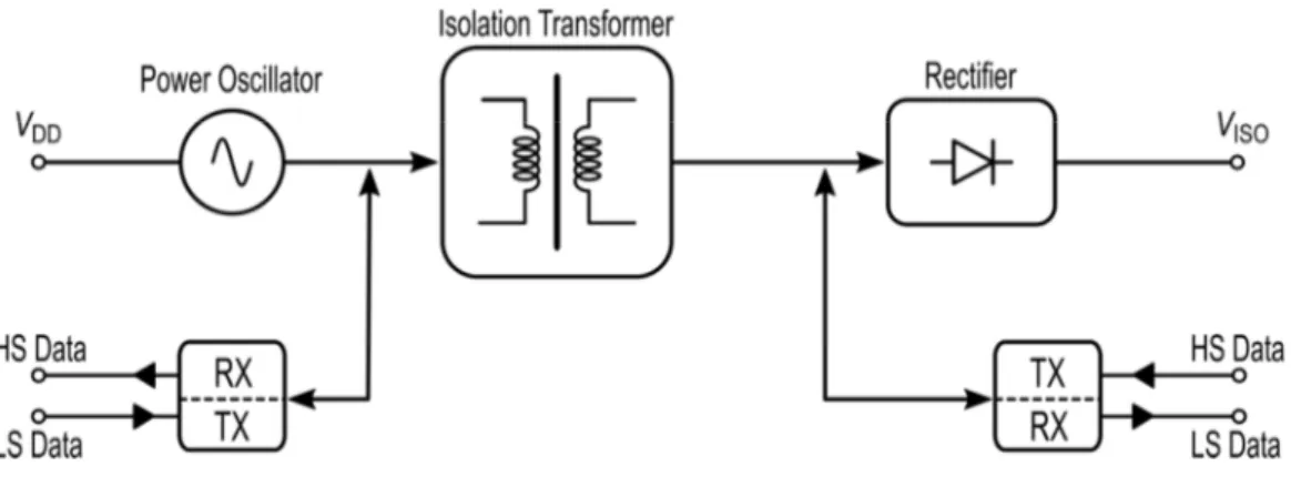
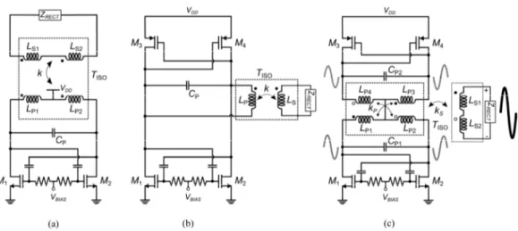
At present the most promising approach for fully integrated dc-dc isolated power converter with data transfer uses architecture exploiting the magnetic coupling. This approach is based on transformer-loaded oscillator that performs the dc-ac power conversion, a planar integrated transformer which guaranteed the galvanic isolation, a rectifier to provide the ac-dc power conversion and data blocks which are able to perform the bi-directional data communication. The key element of these systems is the power oscillator including the integrated isolation transformer which affects the power efficiency performance while driving the choice of the system architecture. In particular, the adopted oscillator is based on
29
current-reuse technique and output power combining, then a three coils-transformers has been implemented. It consists of four inductors for the two primary coils which are arranged through two symmetric interleaved configurations, one for each stacked secondary coil. The thick oxide between the primary and secondary coils guaranteed the galvanic isolation rating up to 5 kV. Since only thin metal layers are available in standard silicon technologies, these windings show very high series resistances, which involves very high operation (VHF) frequencies as well as resonance to improve their poor quality factor (Q-factor) [36].
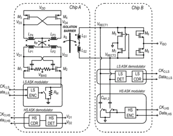
Following these considerations a novel architecture has been conceived for the proposed system and a simplified diagram block is shown in Fig. 1.14.
Figure 1.14 Novel architecture for isolated data and power transfer system
Here, the data and power transfer exploit a single inductive channel to be transferred across the isolation barrier [26]. The dc-dc power converter is a transformer-loaded power oscillator, whose resonant network includes the isolation transformer and the rectifier input impedance. It converts the power supply PDD into ac power PAC for the isolation transformer and hence the rectifier
input. A full-bridge rectifier has been chosen as the simplest balanced topology to perform the ac-dc power conversion, thus converting the ac power at the transformer output into dc available output power POUT for the load, with output
voltage VISO. Each block suffers from power losses which can be expressed by a
30
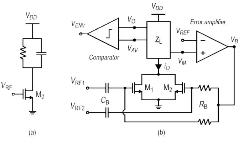
transformer and the power rectifier, respectively. Their product can be used to express the whole power efficiency of the dc-dc power converter, / or simply . As discussed before, the system is also able to perform half-duplex bi-directional data communication. It is performed by using a simple amplitude shift keying (ASK) modulation in order to preserve the peak of the RF control signal. In particular, high-speed (HS) data communication (from isolated sense side to control side) is implemented by means of impedance mismatch at secondary coils of the integrated transformer, while the low-speed (LS) data transmit (from control side to isolated sense side) is implemented by switching a series resistances, thus modulating the oscillation signal of the power oscillator.
Main advantages of this architecture include the use of a single isolation transformer for both isolated power and bidirectional data transfer, thus lowering costs and reducing package and application board sizes.
On the other hand, this architecture is inherently characterised by highly non-linear interactions between each block, which complicate the design. For example, transformer efficiency is highly dependent on the interaction with the driving stage, providing the ac input power, and the cascaded stage, which performs the ac/dc conversion. Moreover, the oscillator is inherently subject to parasitic and input supply variations and do not provide voltage regulation. Finally, the data maximum data rate is not far by the carrier frequency, thus complicating the operations of demodulation.
1.5.2
Technology platform
The technology adopted in this work is a 0.35-µm SOI-BCD technology that features both 3.3-V and 5-V CMOS transistors, a 5-V VHF npn BJT, lateral pnp BJTs and several MOS devices providing high-voltage capabilities through drain-extension techniques [37]. Three Al metal layers with 0.45/0.55/0.9-μm thickness, respectively, and a 3.7-μm thick top Cu layer are available for routing. The process was enriched for this work by a thick-oxide module [38] that was
31
previously developed and characterized for galvanic-isolated data transfer, similar to other state-of-the-art integrated isolators [39], [40], [41]. This module has been recently used for mass-production of several devices providing on-chip galvanic isolation [42], [23]. The tick oxide layer is placed between the two top metal layers, as shown in the simplified back end of line (BEOL) cross-section of Fig. 1.15. Depending on the galvanic isolation rating the tick oxide can have different thickness.
Figure 1.15 Simplified cross-section of the available back end of line with thick
This technology powered by STMicroelectronics was chosen thanks to its compatibility with the thick-oxide module fabrication process and by the high resistivity of the available SOI substrate that is mandatory to achieve high efficiency for power transformers. Is worth noting that, the galvanic isolation rating of this adopted technology has been certified up to 5 kV.
1.5.3
Main results
For the first time a fully integrated CMOS system, able to transfer both data and power on the same isolation transformer was demonstrated. It can be adopted in an interesting real-life application requiring isolated data and power transfer which was addressed during this work as a part of a research project at the
32
RF-ADC, a joint research center between the University of Catania and STMicroelectronics. As outcome, during my permanence at RF-ADC two full integrated system were designed and characterised in the available technology by different design teams, showing measured performance that are competitive with the state of the art.
They are:
• a highly integrated data and power transfer system, with relatively low output power, for autonomous sensors applications [26].
• medium power CMOS dc-dc converter, with output power of 200 mW for power supplies of general purpose circuitry [43].
General purpose circuitry, such as wireline transceivers and signal processing blocks that require lower output power can benefit of these innovative integrate systems, thus lowering costs while using the widespread CMOS devices demonstrated in [43], and as will be disclosed in Appendix A. Autonomous current sensor interfaces require quite low output power, e.g. around 10-25 mW even if leading to use of multiple isolation transformer, thus increasing costs and complexity. The proposed architecture in [26] enabling both data and power transfer by means of a single inductive channel, shows a competitive advantage with respect to the state of the art even if it does not include any circuitry to improve the CMTI. Lastly, in order to overcome this limits a different system architecture can be implemented. It would be able to deliver a regulated output power up to 100 mW, while providing a half-duplex data communication having maximum data rate up to 50 ⁄ and CMTI up to 50 ⁄ . μ
33
2.
Chapter II
Fully integrated galvanically isolated
power transfer systems
This chapter takes on the detail descriptions and the design of a fully integrated dc-dc converter with galvanic isolation in order of several kilovolts, i.e., 5-kV. The converter was designed to produce about 30 mW output power,
POUT, at 3-V output voltage, VOUT, from a 3-V power supply, VDD. To enable a
wide range of low-power applications requiring an isolation barrier, the reduction of cost, complexity and size is a crucial target to be reached. An upper bound of 5 mm2 for the whole area and a novel architecture for dc-ac power converter were chosen as a reasonable specification for the isolated power transfer system. Indeed, the design was customized to the maximization of power efficiency being a crucial aspect for autonomous low-power isolated sensors.
2.1
System description
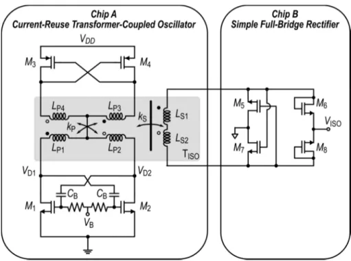
A simplified schematic of the fully integrated isolated dc-dc converter is shown in Fig. 2.1. The integrated transformer, TISO, is the core of the system since
it provides on-chip galvanic isolation and power transfer. In the proposed implementation it is integrated into the chip A with a novel power oscillator circuit exploiting the current-reuse technique, whereas a second die includes a well-known full-bridge rectifier for ac-dc power conversion, and the turn’s ratio of the integrated transformer is used to obtain the required step-up voltage conversation ratio. The power transfer system was fabricated in 0.35-µm BCD-SOI technology providing on-chip galvanic isolation, as described in Section 1.5.2.
34
Figure 2.1Schematic of the fully integrated data and power transfer system
2.2
Design issues
The description fulfilled in this section is helpful to better understand the role of each block including in the power transfer link and the impact of each block parameters on the efficiency of other blocks. For a given output power, the main goal of the design is to maximize the system power efficiency while guaranteeing both small silicon area and proper CMTs rejection, which are crucial specifications in galvanically isolated power transfer systems.
Rectifier is the simplest block providing the ac-dc conversion and showing a well-defined and direct relationship between its sizes, in particular
(i.e., , , , ) and both power efficiency and input capacitance . The transformer gives the main contribution to the whole area of the integrated dc-dc converter (i.e., more than 50 % of the overall silicon area). It also greatly affects the overall power conversion efficiency, thus requiring the maximization of quality factors and magnetic coupling factors. They both depend
35
on the geometrical parameters and the available back-end-of-line (BEOL). Indeed, to maximize the transfer efficiency the operating frequency has to be kept as close to the resonant frequency due to the secondary coil and the input rectifier capacitance.
The oscillator core is the most complex and important block in the power transfer chain. Its non-linear behaviour needs high tank inductance and minimum external capacitance for a given transistor’s width to work with high efficiency. To this aim, the equivalent parallel losses resistance seen at primary side, ≅ ∙ ∙ ∙ 1 + ∙ 1 + have to be maximized. By taking advantage of stand-alone block performance and their relationships, an optimized system design can be achieved. Moreover, these considerations confirm that no significant result can be reached by designing each system block as a stand-alone circuit. Instead, optimum performance can be obtained by adopting an iterative co-design procedure between the dc-dc converter building blocks. Eventually, a proper design strategy is mandatory to perform this co-design due to the large number of free design variables.
2.3
Efficiency analysis and block design of the
isolated dc-dc power converter
The design of this isolated dc-dc power converter poses several challenges since it is characterized by non-linear interactions between each building stage, thus involving system optimization if the output power have to be delivered with high efficiency. In order to achieve high power efficiency while adopting scaled technologies, transformer-loaded oscillators exploiting a current-reuse technique have recently gained attention. In this section each block of the power transfer system will be descripted examining how its efficiency depends on the design parameters of the converter, as well as on the loading effect of the other blocks, to better understand main issues and trade-offs between each building block designed. The overall power system efficiency,
η
, is obviously the product of the36
efficiency of each building block when operated into the whole system. Specifically, the power flow from the power supply, PDD, to the dc power
delivered to the load, POUT, involves losses in the active devices, in the integrated
transformer, and in the rectifier, as detailed in the flow diagram depicted in Fig. 2.2. The total power at the transformer input coils is called PTX while POUT_AC
is the ac power at its output.
Figure 2.2 Power transfer flow diagram
The rectifier efficiency, ηRECT, is defined as / _ , whereas the
efficiency of the integrated transformer, ηTISO, is defined as _ / . We also
define the active core efficiency,
η
CORE, as / , hence:_ (1.1)
_ (1.2)
(1.3) (1.4)
Starting out by the rectifier we analyse the design of each block of the proposed dc-dc power converter with galvanic isolation.
37
2.3.1
Rectifier
The rectifier provides the ac-dc power conversion, thus receiving the
POUT_AC from the isolation transformer it produces the dc output power (POUT).
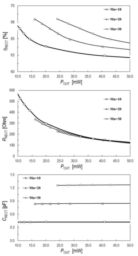
The SOI-BCD technology platform adopted does not include Schottky diodes, hence a simple CMOS full-bridge rectifier was used (see Fig. 2.1). The main parameters of this block are the conversion efficiency ηRECT and its input
impedance, which can be represented as a RC parallel circuit, RRECT//CRECT.
Indeed, the ηRECT depends on both the transistors’ multiplicity (MNMOS) and the dc
output power POUT. The design was focused on the maximization of the
conversion efficiency ηRECT at the required output power, POUT, by setting the
multiplicity MNMOS (i.e., M5,6,7,8). The frequency response of the rectifier
highlights a degradation of its conversion efficiency at increasing frequencies, thus an upper limit to the operation frequency (i.e., the oscillation frequency) was set. The Fig. 2.3 (a) shows ηRECT as a functions of the output power for MNMOS
between 10 and 30 with a 330-MHz input signal and 3-V VOUT. For increasing
power levels a higher number of transistors is required to do not compromise the efficiency performance. The input resistance, RRECT, reported in Fig. 2.3 (b) is
inversely proportional to POUT and does not increase with MNMOS, whereas the
input capacitance, CRECT, shown in Fig. 2.3 (c) is almost constant with MNMOS and
it is independent of POUT. For the sake of clarity, the simulated ηRECT and input
impedance, ZRECT= RRECT//CRECT, for different values of MNMOS at the target
POUT of 25 mW at VOUT = 3 V, are summarized in Table 2.1. It is obvious that for
MNMOS > 20 a small efficiency improvement can be obtained at the cost of
increased rectifier area, input capacitance and, most importantly, routing complexity. We set MNMOS equal to 20 as trade-off between ηRECT and CRECT. This
choice takes into account the fact that this block can easily provide high efficiency when compared to other blocks in the power chain.
38
Figure 2.3 Rectifier efficiency as function of output power for different MNMOS
39
Table 2.1 Simulated rectifier performance, VOUT= 3 V, POUT= 25 mW
MNMOS ηRECT [%] RRECT [Ohm] CRECT [pF] Schematic 10 63.4 248 0.42 15 64.3 236 0.63 20 65.7 234 0.84 25 66.9 224 1.05 30 67.8 220 1.26 post-layout 20 61 228 1.5
Another important design issue is represented by the rectifier layout: parasitic due to metal connections highly affect efficiency performance and the input capacitance, especially when a high number of transistors have to be connected. Main degradation of both efficiency and bandwidth comes from the resistive parasitic, which were minimized by exploiting all the available metal layers (i.e., metal 1 to metal 4 plus alucap) and optimizing the number of vias. Simulations show that for operating frequencies smaller than 400-MHz the rectifier characteristics are quite constant, and thus it was modelled by an input impedance ZRECT of 228 Ohm//1.5 pF for POUT_AC = 25 mW at VOUT = 3V.
2.3.2
Oscillator core
The oscillator performs the dc-ac power conversion by exploiting the isolation transformer as resonant load. It is another key block of an isolated power transfer system since it greatly determines the maximum delivered output power and the overall efficiency. One of the most adopted circuit exploits the well-known cross-coupled nMOS topology as shown in Fig. 2.4 (a), which operating in class D improves the power efficiency.
40
Figure 2.4 Oscillators topologies for isolated power transfer. (a) Class D Oscillator. (b) Complementary cross-coupled oscillator. (c) Current-reuse oscillator
RF class D oscillators have gained attention in highly scaled technologies, for design approaches mainly focused on low power applications [44], thanks to its advantages in term of low phase noise. In fact, this topology makes possible to combine low phase noise, low supply voltage and high efficiency simply by increasing the size of the cross-coupled nMOS switches, thus maximizing the oscillation amplitude. However, this topology requires special devices, such as lateral-diffuses or thick-oxide transistors with higher breakdown voltages, to sustain drain voltages that can reach a pick of approximately 3·VDD. When only a
standard CMOS technology is available, the complementary cross-coupled architecture shown in Fig. 2.5 (b) is used. This solution allows to reduce the power consumption while avoiding breakdown issues [45], being its oscillation level inherently contained within the supply voltage. For small-signal operation it provides higher small-signal trans-conductance for the same biasing current, thanks to the double cross-coupled pair. However, for large-signal operation this advantage is less important, since very high transistor’s width are required to provide ac power with high efficiency and trans-conductance is not a problem. Although the active devices can easily reach the deep triode region to minimize power losses, for power transfer applications the efficiency of this topology is still lower than the class D oscillator, due to lower oscillation level and higher losses in the active devices. Indeed, the differential voltage across the primary coil can
41
be around VDD at most, which entails higher currents in the coil for a given power
level, and during operation two devices are always stacked for each path between power supply and ground, apart from the primary coil, instead of only one. Therefore, novel transformer-loaded topologies are required to improve performance while avoiding breakdown and properly exploiting the characteristics of integrated transformers at the same time. This aspect is particularly important since passive devices are the bottleneck for both power efficiency and power density in standard technology. A novel topology which has been found to satisfy these requirements is shown in Fig. 2.5 (c). It performs three key aspects, i.e. inductively coupled oscillators, current-reuse technique, and output power combining [46]. The circuit is made up of two LC complementary CMOS oscillators, i.e., M1,2-LP1,2 and M3,4-LP3,4, which share the same supply current and
whose tank inductors are magnetically coupled to each other according to the dot-scheme represented in the figure. In particular the inductors LP1,2 and LP3,4
form the two primary windings of the isolation transformer, TISO, whereas
inductors LS1,2 make the second winding. If the magnetic coupling coefficient
between the primary windings, kP, is sufficiently high (typically greater than 0.6)
frequency synchronization of the two oscillators is reached [47], [48]. Thanks to the magnetic coupling between the primary coils, the equivalent load inductance of each oscillator is boosted by the factor (1+kP), while maintaining the same
resistive losses. The signal produced at each primary winding is then delivered to the secondary winding of TISO, where a power combining is performed, thus
nearly doubling the overall output power on the rectifier input. The magnetic coupling between primary and secondary coils, kS, is 0.8. In this configuration
thanks to the current-reuse arrangement, which is easily implemented by means of the central-tap of the primary windings, the further improving of the oscillator power efficiency is allowed. In particular, this architecture compared with the complementary cross-coupled topology, has highlighted an increase for both output power and power efficiency higher than 10 % and 40 %, respectively. This comparison was carried out in the same CMOS process, at equal supply voltage and ZRECT, and for the same frequency oscillation. Moreover, the total
42
transformer, which is a key constraint in this context. It is worth noting that to maximize the power efficiency at the given output power a co-design procedure between the oscillator core and the transformer is required, thus exploiting this procedure we will design the oscillator core.
2.3.3
Isolation transformer
The implementation of the integrated isolation transformer involves the use of a staked configuration for primary and secondary windings. Indeed, the galvanic isolation is guaranteed by the thick oxide layer between the top metal layers (i.e., metal 4 and metal 3) of the adopted technology platform. As discussed in the previous section, the adopted power oscillator based on current-reuse technique requires an adequate magnetic coupling factor kP in order to achieve an
optimized power combining into the third winding. To this aim a three coils-transformer is implemented, as shown in Fig. 2.5. Specifically, the four inductors of the primary windings, LP1-LP4, are arranged through two symmetric interleaved
configurations, LP1/3 and LP2/4, one for each secondary coupled coils (i.e., LS1 and
LS2), with a common terminal for the central-tap.
Figure 2.5 Isolation transformer schematic
Thanks to the minimum spacing (1-µm) available on the metal 3 for LP1/3
and LP2/4 the magnetic coupling is further maximize. Instead the secondary coils,
LS1 and LS2, are built exploiting the metal 4 and they are staked on the primary
43
the underpasses are exploited. These are built by using the shunted lowest metal layers in order to minimize their series resistances. The design of this integrated transformer for the proposed dc-dc power converter needs a co-design procedure with the active component (i.e., oscillator core), which will be discusses in next section. As mentioned before, high coupling factor between primary and secondary coils, kS, is mandatory for an optimized design since a low k-factor
combined with the poor Q-factor of integrated transformers would highly affect the overall system efficiency. Consequently, the maximization of the overlap area between primary and secondary windings is crucial to avoid magnetic coupling factor degradation [49]. To this end, it is of utmost importance to equalize the external diameters of the secondary coils LS1 (LS2) and the interleaved primary
windings LP1-3 (LP2-4), by exploiting a geometrical constrains. Indeed, being such
transformer topology rather complex, in interest of speed-up the design flow a novel lumped, geometrically scalable model was developed.
Figure 2.6 Isolation transformer. (a) Primary windings. (b) Secondary windings. (c) 3D-view