U
NIVERSITÀ DELLA
C
ALABRIA
D
IPARTAMENTO DIC
HIMICAS
CUOLA DID
OTTORATOB
ERNARDINOT
ELESIO-
S
CUOLA DIS
CIENZA ET
ECNICAM^3
-
M
ESOFASI EM
ATERIALIM
OLECOLARIXXV
CICLO
(CHIM-02)
PhD Thesis
N
EW
H
YBRID
S
OLAR
C
ELL
(СNT
–
R
UTHENIUM
D
YE
)
Supervisore Prof. Giovanni DE FILPO
Coordinatore Prof. Carlo VERSACE
Direttore Prof. Roberto BARTOLINO
Candidato
Dott. Svetlana SIPROVA
N
EW
H
YBRID
S
OLAR
C
ELL
(СNT
–
R
UTHENIUM
D
YE
)
ACKNOWLEDGEMENTS БЛАГОДАРНОСТЬ
I would like to express deepest appreciation to administration of the Doctoral School of Science and Technique “Bernardino Telesio” for the given possibility of the education and to professors of School for the given knowledge and collaboration.
I would like to thank my supervisor, Professor Giovanni De Filpo. I thank Professor Giuseppe Chidichimo for the collaboration, consultations and the support.
Я бы хотела выразить благодарность за сотрудничество и поддержку коллективу Российско-Итальянского центра по применению интеллектуальных материалов Научно-Исследовательской Части Нижегородского Государственного Университета им. Н.И. Лобачевского, особенно профессору Машину Александр Ивановичу и научному сотруднику Нежданову Алексею Владимировичу. Выражаю мою особую благодарность сотрудникам Учреждения Российской академии наук Института металлоорганической химии им. Г. А. Разуваева РАН, А.М. Объедкову и , за сотрудничество и синтез необходимых образцов для экспериментальной части Chapter V. Я благодарю моих родителей, Сипровых Виктора Ивановича и Галину Петровну, а так же близких родственников, за моральную поддержку и непрерывное общение в течение моего трех летнего пребывания в Италии. А.И. Кириллову
CONTENTS ABSTRACT 3 CHAPTER I INTRODUCTION 4 REFERENCES 6 CHAPTER II SOLAR CELL 7
2.1 Steps of the development of the solar power engineering and of
photovoltaic devices. 7
2.2 Prototypes of our system: Gratzel Cell and Amaratunga cell. 13 2.3 Materials for the fabrication of the solar cell. 16
REFERENCES 19
CHAPTER III
EXPERIMENTAL PART AND DATA DISCUSSION
STUDIES OF DIFFERENT METHODS OF THE FABRICATION OF
THE FUNCTIONAL LAYER OF THE SOLAR CELL 22
3.1 Reproduction of Amaratunga cell. Current-Voltage Characteristics. 22 3.2 Spray deposition of the functional layer. Variations of the PO3T
concentration. CVC. 24
3.3 ITO and FTO electrodes. 26
3.4 Changing of dye. Molecule-bridge – PyreneMethanol. 27 3.4.1 Comparison of methods of the deposition and of variations of
the composition in suspension. 29
3.4.2 Comparison of different electrodes. 32
3.4.3 The dimension of the sample. 33
3.4.4 Amount of the functional layer on the electrode. 34
REFERENCES 37
CHAPTER IV
EXPERIMENTAL PART AND DATA DISCUSSION
ELECTROPHORESIS 38
4.1 Preparation of SWNTs for electrophoresis. 38
4.2 Process of electrophoresis. The fabrication of the cell. 39 4.3 Current-Voltage Characteristics. SEM measurements. 40
REFERENCES 42
CHAPTER V
EXPERIMENTAL PART AND DATA DISCUSSION
5.1 Formation of nanostructured composition materials based on Multiwalled Carbon Nanotubes by Metal-Organic Chemical Vapor
Deposition. Synthesis. 43
5.2 Flat MOCVD samples with MWNTs. Thickness. Absorption. 46 5.2.1 Fabrication of the cell. Current-Voltage Characteristics. 49 5.3 Cell with PEDOT-PSS as oxidation-reduction part of the cell. 53
5.4 Cylinders. Cutting. 56
5.4.1 Fabrication of the cell. Current-Voltage Characteristics. 59
REFERENCES 60
ABSTRACT
Negli ultimi anni le applicazioni dei nanotubi di carbonio nel settore microelettronico sono notevolmente aumentate date le proprieta’ uniche. In particolare la conducibilita’ dei nanotubi fa si che essi trovino interessanti utilizzi nel settore fotovoltaico. Questo lavoro si concentra sulla progettazione di una cella solare ibrida a base di nanotubi di carbonio e dye di Rutenio.
Nella prima parte sono stati studiati diversi metodi di realizzazione dello starto omogeneo di nanotubi come starto conduttivo della cella. E’ stata proposta la molecola 1-Pyrenemethanol che contiene i gruppi pirenico e ossidrilico, per creare il contatto tra i nanotubi ed il dye.
Nella seconda parte del lavoro lo starto di nanotubi e’ stato formato mediante elettroforesi per single-walled nanotubes (SWNTs) e metal-organic chemical vapor deposition (CVD) per multi-walled nanotubes (MWNTs). Entrambi i metodi hanno dato la possibilita’ di creare campioni con ampia area superficiale, dai quali sono state fabbricate le celle solari. Sono state studiate determinate le dipendenze tra i fattori dei metodi e le proprieta’ delle celle prodotte.
CHAPTER I
INTRODUCTION
Every year the energy consumption continues to rise because of the development of industry and the population upsurge. Given that main energy resources are limited, it will be a significant challenge in the future. Therefore it the last decade, the science has worked to increase the use of renewable sources of energy such sunlight, wind, rain, tides, and geothermal heat. Renewable energy is an alternative to fossil fuels and was commonly called alternative energy in the 1970s and 1980s. In 2009, about 16% of global final energy consumption came from renewable energy. At the end of 2011, cumulative global photovoltaic (PV) installations surpassed 69 GW, an increase of almost 70% [1], and PV power stations are commonplace in Germany, Italy, and Spain. Climate change concerns, coupled with high oil prices, peak oil, and increasing government support, are driving increasing renewable energy legislation, incentives and commercialization.[2] It also has the advantage that it lasts for as long as we are on the planet, vs. less than a century for most of the non-renewable resources. Conventional production of oil peaked in 2006, and the more we use it the faster it will be depleted.
The total solar energy absorbed by Earth's atmosphere, oceans and landmasses is approximately 3,850,000 exajoules (EJ) per year. Solar photovoltaics is now, after hydro and wind power, the third most important renewable energy source in terms of globally installed capacity. Photovoltaics can generate electricity for a wide range of applications, scales, and climates; it is a cost-effective way to provide power to remote areas and for space applications [3]. Table 1.1 lists some of the technical, economical and infrastructural features of photovoltaics, showing that photovoltaics help us avoid most of the threats associated with our present techniques of electricity production and also has many other benefits [4].
Table 1.1 Advantages and disadvantages of photovoltaics.
Advantages Disadvantages
Fuel source is vast and essentially infinite No emissions, no combustion or radioactive fuel for disposal (does not contribute perceptibly to global climate change or pollution)
Low operating cots (no fuel) No moving parts (no wear)
Ambient temperature operation (no high temperature corrosion or safety issues) High reliability in modules (>20 years) Modular (small or large increments) Quick installation
Can be integrated into new or existing building structures
Can be installed at nearly any point-of-use Daily output peak may match local demand
High public acceptance Excellent safety record
Fuel source is diffuse (sunlight is a relatively low density energy)
High installation costs
Poorer reliability of auxiliary (balance of system) elements including storage
Lack of widespread commercially available system integration and installation so far
Lack of economical efficient energy storage.
The enormous gap between the potential of solar energy and our currently slight use of it is due to the modest energy density of the radiation, low conversion efficiencies of photovoltaics, and cost of materials currently required. The cost effective raising of conversion efficiency is primarily a scientific challenge: breakthroughs in fundamental understanding enable the development of materials and methods leading to the photovoltaic market progress [3]. The modern era of photovoltaic device technology moves in a direction of easy fabrication and cheap compounds as organic materials. Now science increases methods of development of dye-sensitized solar cells (DSSC) [5, 6], organic cells [7, 8], organic tandem cells [9], hybrid cells [10].
This work contains studies of methods of fabrication of the new hybrid solar cell based on carbon nanotubes (CNTs) and metal-organic dye with Ruthenium. There are
considered methods of the forming of NT layer to obtain the positive results from final produced photovoltaic cell, and to determine the dependence between parameters of fabrication and properties of the cell.
REFERENCES
1. K. Ardani, R. Margolis The 2010 Solar Market Trends Report. U.S. Department of Energy. 2011.
2. C.Greenwood, A. Hohler and et al. Global Trends in Sustainable Energy Investment 2007. United Nations Environment Programme. 2007.
3. N.V. Yastrebova. High-efficiency multi-junction solar cells: Current status and future potential. University of Ottawa. 2007.
4. A. Luque, S. Hegedus. Handbook of photovoltaic science and engineering. 2003. 5. M. Grätzel. Journal of Photochemistry and Photobiology C: Photochemistry Reviews,
2003, 4 (2), pp. 145–153.
6. M. Grätzel. Inorganic Chemistry, 2005, 44 (20), pp. 6841–6851. 7. D. Wöhrle, D. Meissne. Advanced Materials, 1991, 3 (3), pp. 129–138. 8. A. Yakimov. Applied Physics Letters, 2002, 80 (9), pp. 1667 – 1669.
9. T. Ameri, G. Dennler. Energy & Environmental Science, 2009, 2 (4), pp. 347-363. 10. W.U. Huynh, J.J. Dittmer and et al. Science, 2002, 295 (5564), pp. 2425-2427.
CHAPTER II
SOLAR CELL
The aim of this chapter is to show a general concept of fabrication and operation of Solar Cells (SC). The operation of SC always based on the photovoltaic effect (PVE). The photovoltaic effect is the creation of voltage or electric current in a material upon exposure to light ([1]), it is the conversion of sunlight into electricity. Sunlight is composed of photons - particles of solar energy, they have no mass, but carry sizeable amount of energy. The amount of energy of every photon corresponds to the different wavelengths of the solar spectrum. When photons strike a SC, they may be reflected or absorbed, or they may pass right through. The absorbed photons generate electricity. The energy of a photon is transferred to an electron in an atom of the photovoltaic device. With its newfound energy, the electron is able to escape from its normal position associated with a single atom in the semiconductor to become part of the current in an electrical circuit (fig.2.1). Special electrical properties of the SC a built-in electric field provide the voltage needed to drive the current through an external load [2].
–
+
Band gap Conduction Band Valence Band hυ > BGFigure 2.1 The illustration of the photovoltaic effect in semiconductor.
2.1. Steps of the development of the solar power engineering and of photovoltaic devices.
The first in practice photovoltaic effect was discovered in 1839 by Alexandre Edmond Becquerel [3], a young experimental physicist in France at age of 19, while
assisting his father, experimenting with electrolytic cells made up of two metal electrodes [4]. In theory this effect was described only in 1904, when Albert Einstein publishes his pioneering theoretical work on the photoelectric effect, and he receives the Nobel Prize in physics in 1921 for this work [4]. After these two great steps started age of Photovoltaic Cells (PVC). In 1931 A.F. Ioffe guides a project at the Physico-Technical institute in St.Petersburg on thallium sulphide photocells, which reach a record efficiency at that time of more than 1%. In 1953 G.Pearson at Bell Labs (New Jersey, USA) begins research of Li-doped Si solar cells. In 1954, the first modern solar cell was invented at Bell Laboratories with an efficiency 6%. In 1960, Hoffmann Electronics makes a jump to 14% efficient PV cells, mainly used for satellite technology and space applications. In 1970, first highly effective GaAs heterostructure solar cells are created by Zhores Alferov and his team in the USSR. In 1976, David Carlson and Christopher Wronski of RCA Laboratories create first amorphous silicon thin-film solar cell, which have an efficiency of 1.1%. In 1980, the Institute of Energy Conversion at University of Delaware develops the first thin-film solar cell exceeding 10% efficiency using Cu2S/CdS technology. 1985 – 20% efficient silicon cell are created by the Centre for Photovoltaic Engineering at the University of New South Wales. Later the Cathedral of Magdeburg installs solar cells on the roof, marking the first installation on a church in East Germany at 1990. At the moment efficient photoelectrochemical cells are developed, the dye-sensitized solar cell is invented (1991). 1994 – NREL develops a GaInP/GaAs two-terminal concentrator cell (180 suns) which becomes the first solar cell to exceed 30% conversion efficiency. 1996 – The National Center for Photovoltaics is established. Gratzel, École Polytechnique Fédérale de Lausanne, Lausanne, Switzerland achieves 11% efficient energy conversion with dye-sensitized cells that use a photoelectrochemical effect. 2007 - New World Record Achieved in Solar Cell Technology – 42.8% efficiency achieved by University of Delaware [5].
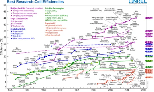
The National Renewable Energy Laboratory (NREL) presents the statistic diagram of the progress with time of the solar energetics “Best Research – Cell Efficiencies” every year (fig.2.1.1). The statistic diagram contains five general groups of solar cell kinds: multijunction cells; single-junction GaAs cells; crystalline Si cells; thin-film cells; emerging photovoltaic cell.
Figure 2.1.1 Presents the statistic diagram of the progress with time of the solar
energetics (NREL) [6].
Multijunction cells. The highest-efficiency solar cells use multiple materials
with bandgaps that span the solar spectrum [7]. Multi-junction solar cells consist of some single-junction solar cells stacked upon each other, so that each layer going from the top to the bottom has a smaller bandgap than the previous, and so it absorbs and converts the photons that have energies greater than the bandgap of that layer and less than the bandgap of the higher layer (fig.2.1.2.) [8]. Multi-junction solar cells experience a fundamental limitation relating to the availability of materials with optimal band gaps that simultaneously allow high efficiency through low defect densities. Alloys of groups III and V of the periodic table are good candidates for fabricating such multijunction cells: their bandgaps span a wide spectral range, and most of the bandgaps have direct electronic structure, implying a high absorption coefficient, and their complex structures can be grown with extremely high crystalline and optoelectronic quality by high-volume growth techniques [9, 10].
Figure 2.1.2 Multi-junction energy diagram. Semiconductors with different bandgaps
quasi-Fermi levels defining the open-circuit voltage are indicated by the horizontal blue dashed lines. The yellow dots represent the electrons [11].
Multi-junction solar cells have been studied since 1960 [12]. The first multi-junction device was demonstrated in early 1980s, and it converted 16% of the solar energy into electricity [13]. In 1994, US National Renewable Energy Laboratory (NREL) broke the 30% barrier. A present-day record 40.7% efficiency was achieved with a triple-junction version of the cell [14]. However, this efficiency is gained at the cost of increased complexity and manufacturing price. To date, their higher price and lower price-to-performance ratio have limited their use to special roles, notably in aerospace where their high power-to-weight ratio is desirable. In terrestrial applications these solar cells are used in concentrated photovoltaics (CPV) with operating plants all over the world. The maximum theoretical limit efficiency of multi-junction solar cells is 86.8% [15].
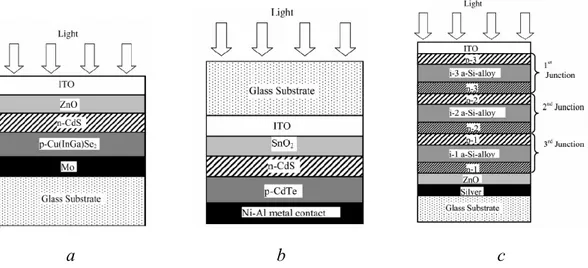
Thin-film cells. In principle, a thin-film solar cell (TFSC) is a junction device
obtained by placing two electronically dissimilar materials together with a thin electronic barrier in between to separate charge [16]. However, efficient devices must ensure high conversion efficiency of solar photons and high collection efficiency of excited charge carriers. A variety of junctions such as Schottky barrier, homojunction and heterojunction have been studied. Junctions can be abrupt, graded, buried, heteroface, etc., involving materials of different conductivity/ type of conductivity [17]. Typical examples of the cross-section of various junctions, Cu(InGa)Se2, CdTe/CdS, triple junction p-i-n a-Si:H are shown in Figure 2.1.3.
a b c
Figure 2.1.3 Typical TFSC structures for single-junction: a - substrate Cu(InGa)Se2; b - superstrate CdTe; c - tandem a-Si triple-junction devices.
Different junction devices with appropriately graded band-gap can be placed in tandem, or can be integrated to form a multijunction device [18]. Theoretically, if all solar photons can be converted to electricity, one may approach thermodynamic Carnot cycle efficiencies [19]. Theoretical analysis shows that 53% efficiency can be achieved with four junction devices and as the number of junctions goes to infinity [20], the efficiency can reach as high as 68%. In view of the difficulty and complexity of fabricating such optoelectronically matched junctions, commercial devices with up to only three junctions have been in production for a-Si:H [21] and GaAs–based [22] devices. This is made possible by the fact that in these cases band-gap tailoring with additives/dopants is conveniently achieved. By using multijuction device structure in a:Si-H tandem solar cells, relatively more stable and higher-efficiency devices with a minimized Staebler–Wronsky degradation effect [23] are fabricated [24].
Innovative device structures that employ mesoporous TiO2 films change the concept of two distinctive p and n layers conventionally used to form p–n junction devices. Extremely thin absorber (ETA) solar cells use TiO2 mesoporous films embedded with organic and inorganic absorber materials. These device structures are designed to improve the effective charge carrier separation within the absorber materials and to enhance the light absorption due to its scattering abilities [25]. Plastic/organic solar cell devices employ blend cell structure in addition to the conventional layered structure. In a blend cell, the molecule mixing occurs on a scale that allows good contact between molecules. This increases the interface area of charge percolation and allows most excitons to reach the donor/acceptor interface. Typical structures of an ETA and blended plastic solar cells are shown in Figure 2.1.4. Several blend structures have been proposed that include polymer-blend [26],TiO2-blend [27],C60-blend [28] and nanorod-blend [29]. However, an ideal device structure suitable for high-efficiency devices is yet to be identified.
a b
Figure 2.1.4 Innovative TFSC structures: a – mesoporous device structures for ETA
solar cells (adopted from Reference 25), b – organic blend cells. MDMO-PPV (poly)[2-methyl, 5-(3*, 7** dimethyl-octyloxy)]-p-phenylene vinylene); PCBM ([6,6]-phenyl C61 butyric acid methyl ester).
Emerging photovoltaic cell. Emerging Photovoltaic Technology embraces
dye-sensitized solar cells (DSSC), various types of organic cells, organic tandem cells, inorganic cells, hybrid cells. Our project concentrated on DSSC and hybrid cell, then these types of solar cell will be discussed in detail in the following paragraph.
2.2. Prototypes of our system: Gratzel Cell and Amaratunga Cell.
Below we consider two types of solar cell: Gratzel Cell [30] and Amaratunga Cell [31]. These are two systems which we took as prototypes of our cell.
A dye-sensitized solar cell (DSSC) [32] is a low-cost solar cell belonging to the group of thin film solar cells. It is based on a semiconductor formed between a photo-sensitized anode and an electrolyte, a photoelectrochemical system. The modern version of a dye solar cell, also known as the Gratzel cell, was originally co-invented in 1988 by Brian O'Regan and Michael Gratzel at the University of Berkley and this work was later developed by the aforementioned scientists at the École Polytechnique Fédérale de Lausanne until the publication of the first high efficiency DSSC in 1991 [33]. M. Gratzel has been awarded the 2010 Millennium Technology Prize for this invention.
A dye-sensitized solar cell can be considered as a hybrid version of photogalvanic cells and solar cells based on semiconductor electrodes. The cell consists of a dye-coated semiconductor electrode and a counter electrode arranged in a sandwich configuration and the inter-electrode space is filled with an electrolyte containing a redox mediator (A/A-). The Gratzel cell has a polypyridine complex of Ru as the dye, TiO2 as the semiconductor and (I2/I-3) as the redox mediator. The key reactions taking place in a dye-sensitized photoelectrochemical solar cell are shown schematically in Fig. 2.2.1b. Optical excitation of the dye with visible light leads to excitation of the dye to an electronically excited state that undergoes electron-transfer quenching, injecting electrons into the conduction band of the semiconductor:
S
*-> S
++ e
-cb (1)The oxidized dye is subsequently reduced back to the ground state (S) by the electron donor (A-) present in the electrolyte filling the pores:
S
++ A
--> S + A
(2)
The electrons in the conduction band collect at the back collector electrode and subsequently pass through the external circuit to arrive at the counter electrode where they effect the reverse reaction of the redox mediator:
The net effect of visible light irradiation is regeneration of the dye, the redox mediator and the driving of electron through the external circuit. The process thus leads to direct conversion of sunlight to electricity. If above cited reactions alone take place, the solar cell will be stable, delivering photocurrents indefinitely. The maximum photovoltage obtainable will be the difference between the Fermi level (conduction band) of the semiconductor under illumination and the redox potential of the mediating redox couple. The photocurrent obtainable is a complex entity depending on the spectral, redox properties of the dye, efficiency of charge injection and structural properties of the semiconductor electrode to collect and channel the electrons through the external circuit [30].
a
b
Figure 2.2.1 A schematic presentation of architecture (a) and of key reactions (b) taking
The Gratzel Cell is studied during 20 years. There were tested different dyes, electrolytes, auxiliary molecules. Now the power conversion efficiency (PCE) of Gratzel Cell is more of 13%. Gratzel Cell is the best system for start point of the departure to fabricate the our hybrid cell.
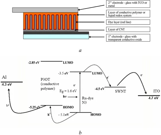
The other type of solar cell which we consider is Amaratunga Cell [31]. Amaratunga and coworkers have been studying new kinds of solar cells constituted of carbon nanotubes (the semiconductor), a dye (which absorbs the light) and a polymer (which transfers electrons to the dye). The efficiency of this type of cells is still rather low, but the materials employed and the procedures used for the construction of the cell are readily available and not expensive. There were poly(3-octylthiophene) (P3OT) as the photoexcited electron donor which is blended with pure single-walled nanotubes (SWNTs) as well as with N-(1-pyrenyl)maleimide (PM) functionalized SWNTs to fabricate photovoltaic cell ITO/P3OTSWNTS+PM/Al (fig 2.2.2). The choice of dye was based on the possibility of its attachment to the SWNT surface (fig 2.2.3) and its photoabsorption spectrum which is well matched to the peak power region in the solar spectrum.
Figure 2.2.2 A schematic illustration of device architecture of Amaratunga Cell
(Indium Tin Oxides - ITO)
Figure 2.2.3 Chemical structure of poly(3-octylythiophene) (P3OT), single-walled
nanotube (SWNT), N-(1-pyrenyl)maleimide, detailed scheme of the dye molecule (PM) attachment to the SWNT surface via π-stacking.
The efficiency of this type of cells is still rather low, but the materials employed and the procedures used for the construction of the cell are readily available and not expensive. Therefore, Amaratunga cell is the next prototype for the developing of new generation cells.
The new hybrid solar cell must contain positive best points of both models, SWNTs as conductive material and Ru-dye for photogeneration of carriers of charge. For it we are going to look components of both cells at greater length.
2.3. Materials for the fabrication of the solar cell.
The hybrid solar cell must contain three basic parts: the dye for absorption of light and photogeneration of carriers; conductor or semiconductor for the charge transfer; p-type organic material or redox system for the reduction of charges.
Gratzel cell contain the ruthenium dyes like N3 (Aldrich Prod. No. 703206) or N719 (Aldrich Prod. No. 703214) (fig.2.3.1a,b). Amaratunga cell has the N-(1-pyrenyl)maleimide (PM) as dye molecule (fig.2.3.1c).
a b c
Figure 2.3.1 Chemical structure of dyes: a – N3; b – N719 [34]; c – PM.
The Ru-dye has larger absorption spectrum them PM (fig.2.3.2), it is preferable dye for our cell. But for the charge transfer we think to take SWTNs is better, because SWNTs have Brunauer-Emmett-Teller (BET) surface area up to 1600 m2/g [35]. It is 8
times more them for TiO2 or ZnO particles (200 m2/g). So this fact gives the advantage for our cell.
a b
Figure 2.3.2 Absorptions of dyes: a - N3 [36]; b – PM [37].
The reduction of charges can be realized by group of conductive polymers [38, 39] or by group of liquid electrolytes [40]. For Gratzel cell the electrolyte contains a redox mediator (I2/I-3). Iodine is very active and destructive element, so the structure of cell can be break down. The other negative point of iodine electrolyte is that it is easily vaporable liquid then evaporation can lead to destruction of the cell. Therefore, it is better to use the conductive polymer like P3OT or Poly(3,4-ethylenedioxythiophene)-poly(styrenesulfonate) (PEDOT:PSS) (fig.2.3.3) [41].
a b
The ideal structure of our hybrid solar cell must be the film of aligned SWNTs covered by Ru-dye and conductive polymer (fig.2.3.4a).
1st electrode - glass with transparent conductive oxide Dye layer (red line) Layer of conductive polymer or liquid redox system 2nd electrode - glass with TCO or
metal
Layer of CNT
a
b
Figure 2.3.4 The schematic illustration of ideal architecture of our hybrid solar cell (a).
REFERENCES
1. A. Goetzberger, C.Hebling. Materials Science and Engineering R, 2003, 40, pp. 1-46. 2. P. Rappaport. Solar Energy, 1959, 3 (4), pp. 8–18.
3. A.E. Becquerel. Comptes rendus de l'Académie des sciences, 1839, 9, pp. 561-567. 4. V. Petrova-Koch, R. Hezel and et al. High-efficient low-cost photovoltaics: recent
developments. Springer Series in Optical Science. New York. 2009.
5. A. Barnett anr et al. 22nd European Photovoltaic Solar Energy Conference (Milan, Italy, 2007), pp. 95-100.
6. “Best Research – Cell Efficiencies” http://www.nrel.gov/ncpv.
7. N.V. Yastrebova. High-efficiency multi-junction solar cells: Current status and future potential. University of Ottawa. 2007.
8. B. Burnett, The basic physics and design of III-V multijunction solar cells, Denver, Colorado. 2002.
9. M. Yamaguchi. Proceeding of 17th Photovoltaic European Conference (WIP, Munich/ETZ, Florence, 2001), p. 2144.
10. R. R. King. Proceeding of International Conference on Solar Concentrators for the Generation of Electricity or Hydrogen (Scottsdale, Arizona, 2005).
11. A. Polman, H.A. Atwater. Nature Materials. 2012, 11, pp. 174–177.
12. M. Wolf. Proceedings of the Institute of Radio Engineers. 1960, 48 (7), pp. 1246-1263.
13. A. Luque, S. Hegedus. Handbook of photovoltaic science and engineering. 2003. 14. Spectrolab solar cell breaks 40% efficiency barrier, December 7, 2006,
http://www.insidegreentech.com/node/454.
15. W.U. Huynh, J.J. Dittmer and et al. Science. 2002, 295, pp. 2425–2427.
16. K. L. Chopra, P. D. Paulson and et al. Thin-Film Solar Cells: An Overview, Progress in Photovoltaics Research and Applications. 2004; 12:69–92 (DOI: 10.1002/pip.541).
17. A.L. Fahrenbruch, R.H. Bube. Fundamentals of Solar Cells. Academic Press: New York, 1983.
18. T.J. Coutts, K.A. Emery and et al. Progress in Photovoltaic: Research and
19. A.D. Vos. Endoreversible Thermodynamics of Solar Energy Conversion. Oxford University Press: Oxford, 1992.
20. M.A. Green et al., Solar cell efficiency tables (Version 29), Progress in Photovoltaics, 2007.
21. J. Yang, A. Banerjee and et al. Proceedings of the 1st World Conference on Photovoltaic Energy Conversion (Hawaii, 1994). pp. 380-385.
22. R.R. King, J.H. Ermer and et al. Proceedings of the Space Power Workshop, 2001.
23. D.L. Staebler, C.R Wronski. Applied Physics Letters. 1977, 31(4), pp. 292–294.
24. S. Guha, J. Yang. IEEE Transactions on Electron Devices. 1999, 46, pp. 2080– 2085.
25. I. Kaiser, K. Ernst and et al. Solar Energy Materials and Solar Cells. 2001; 67(1–4), pp. 89–96.
26. A.C. Arias, N. Corcoran and et al. Applied Physics Letters. 2002, 80, pp. 1695– 1697.
27. Q. Fan, B. McQuillin and et al. Chemical Physics Letters. 2001, 347, pp. 325–330.
28. N.S. Sariciftci, L. Smilowitz and et al. Science. 1992, 258, p.1474.
29. W.U. Huynh, J.J. Dittmer and et al. Science. 2002, 295, pp. 2425–2427.
30. K. Kalyanasundaram, M. Gratzel. Coordination Chemistry Reviews. 1998, 77, pp. 347-414.
31. S. Bhattacharyya, E. Kymakis, and G. A. J. Amaratunga. Chemistry of Materials. 2004, 16, pp. 4819-4823.
32. H. Wan. Dye Sensitized Solar Cells. University of Alabama. 2004. 33. B. O'Regan, M. Gratzel. Nature. 1991, 353 (6346), pp. 737–740.
34. K. Kalyanasundaram, M. Grätzel. Material Matters. Aldrich Chemical. 2009, 4(4), pp. 88-91.
35. S. Agnihotri, J.P.B. Mota. Langmuir. 2005, 21, pp. 896-904.
36. L.C.T. Shoute, G.R. Loppnow. Journal of the American Chemical Society. 2003,
125 (50), pp. 15637 15646.
38. W.U. Huynh, J.J. Dittmer. Science. 2002, 295 (5564), pp. 2425-2427. 39. S.I. Na, S.S. Kim. Advanced Materials. 2008, 20 (21), pp. 4061–4067.
40. P. Wang, S.M. Zakeeruddin. Journal of the American Chemical Society. 2003, 125 (5), pp. 1166–1167.
41. C.J. Brabec, V. Dyakonov, J. Parisi, N. Serdar. Organic Photovoltaics: Concepts and Realization. Springer, 2003.
CHAPTER III
EXPERIMENTAL PART AND DATA DISCUSSION
STUDIES OF DIFFERENT METHODS OF THE FABRICATION OF THE FUNCTIONAL LAYER OF THE SOLAR CELL
3.1. Reproduction of Amaratunga cell. Current-Voltage Characteristics.
For the first step we had tried to create photo-electric system on the basis of single walled nanotube (SWNT), dye N-(1-pyrenyl)maleimide (PM) (fig.3.1.1a) and conductive polymer poly(3- octylythiophene) (P3OT) (fig.3.1.1b) – Amaratunga system [1]. Glass with Indium Tin Oxides (ITO) layer is a substrate and an electrode, on it the SWNTs were deposited and covered with polymer P3OT, the layer of aluminum is the second electrode. The structure and architecture of cell showed on figure 3.2.
a b
Figure 3.1.1 a - N-(1-pyrenyl)maleimide; b - poly(3- octylythiophene).
a b
Figure 3.2.1 a - chemical structures of components; b – schematic illustration of
The functional layer was deposited on the glass from the mixture. Preparation of mixture was: the PM solution in chloroform (2 mg/ml) had been added to the chloroform suspension of the nanotubes (0,22mg/ml) and sonicated for a long time, more than 8 hours, following it was blended with P3OT chloroform solution (10mg/ml). The final mixture was sonicated for about 10 hours. Four samples were fabricated by different principles (table 3.1). All samples were dried at 50 oC for 1 hour and were coated with a layer of Al by plasma spraying (Power = 130 W, pressure = 3.4x10⁻² mB, time = 5 min). We checked for the presence of photovoltaic effect in the created samples by Source Meter System 2601 (Keithley). Curent-voltage characteristics (CVC) and description of peculiarities of samples are in the table 1.
Table 3.1 Peculiarities of forming of samples and their CVCs.
Sample A
Mixture was put on the glass with ITO by spin coater at
1000 r.p.m. for 20 sec. -1,8 -1,5 -1,2 -0,9 -0,6 -0,3 0,0 -0,2 -0,1 0,0 0,1 V, mV sample A I, mkA Sample B
Mixture was put on the glass with ITO by independent evaporation of chloroform. 0 2 4 6 8 -0,8 -0,7 -0,6 -0,5 -0,4 -0,3 -0,2 -0,1 0,0 0,1 V, mV I, A Sample C
Mixture was put on the glass with ITO by spin coater at 1000 r.p.m. for 20 sec. Then the first layer was covered with a second layer of P3OT, which was made by independent evaporation of chloroform. 0 25 50 75 100 125 150 175 -4,0 -3,5 -3,0 -2,5 -2,0 -1,5 -1,0 -0,5 0,0 0,5 V, mV I, A
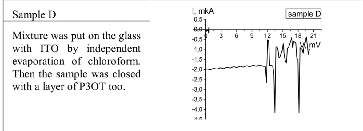
Sample D
Mixture was put on the glass with ITO by independent evaporation of chloroform. Then the sample was closed with a layer of P3OT too.
0 3 6 9 12 15 18 21 -4,5 -4,0 -3,5 -3,0 -2,5 -2,0 -1,5 -1,0 -0,5 0,0 0,5 V, mV sample D I, mkA
Table 3.2 Result of measurements of CVCs of samples A, B, C, D.
A B C D
Area, cm2 12,92 10,15 12,21 13,3 Isc, µA/cm2 - 0.07 0.29 0,15
Voc, mV - 7 153 20
Some of the samples have typical CVC for solar elements. But the values of a short-circuit current (Isc) and of open-circuit voltage (Voc) are very low. Many parameters can influence on the PV effect, such as the thickness of the basic film, or aluminum film, and mostly by the layer of ITO that should be uniformly closed by SWNT-dye layer. The main point of this experiment is that we can observe that the system works and we can try to improve this effect.
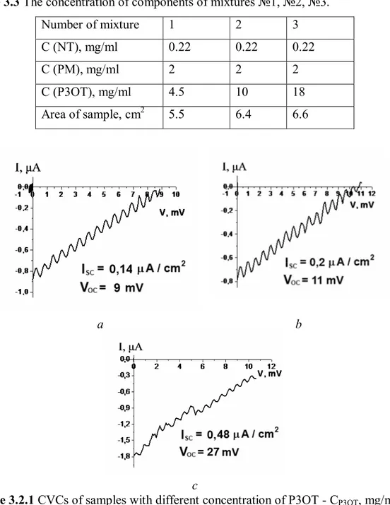
3.2. Spray deposition of functional layer. Variations of the PO3T concentration. CVC.
Spin coater covers the substrate with a very thin layer. Therefore we have changed the method of deposition of a film. Also we have tested lower (4.5 mg/ml) and higher (18 mg/ml) concentrations of P3OT. Three mixtures were prepared with same method. The concentration of components is in table 3.3. Samples were fabricated for every mixture by independent evaporation of chloroform on the ITO glass. Cells have Al layer as second electrode. CVC of samples showed on figure 3.2.1.
Table 3.3 The concentration of components of mixtures №1, №2, №3. Number of mixture 1 2 3 C (NT), mg/ml 0.22 0.22 0.22 C (PM), mg/ml 2 2 2 C (P3OT), mg/ml 4.5 10 18 Area of sample, cm2 5.5 6.4 6.6 a b c
Figure 3.2.1 CVCs of samples with different concentration of P3OT - CP3OT, mg/ml: a – 4.5; b – 10; c – 18. 4 6 8 10 12 14 16 18 0 10 20 30 CP3OT, mg/ml V, mV 4 6 8 10 12 14 16 18 0,0 0,1 0,2 0,3 0,4 0,5 CP3OT, mg/ml Isc, A/cm2 a b
Figure 3.2.2 The dependence of the open-voltage (a) and the dependence of the
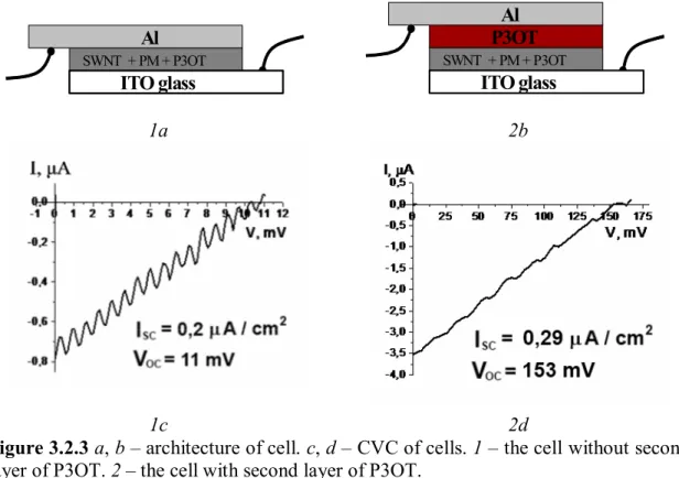
From the results of the experiment it was determined that with growth of concentration of P3OT it increase of open-voltage and shot-current of solar cell. To improve properties of SC we tried to create the auxiliary layer of P3OT, the second layer of pure P3OT from solution 18 mg/ml in chloroform, which was placed on the top of the basic film (fig.3.2.3).
SWCNT + Dye N3 Al SWNT + PM + P3OT ITO glass SWCNT + Dye N3 P3OT Al SWNT + PM + P3OT ITO glass 1a 2b 1c 2d
Figure 3.2.3 a, b – architecture of cell. c, d – CVC of cells. 1 – the cell without second
layer of P3OT. 2 – the cell with second layer of P3OT.
The second layer of P3OT positively influences the open-voltage of cell, it increases by 14 times. The auxiliary layer of P3OT will be placed in next samples.
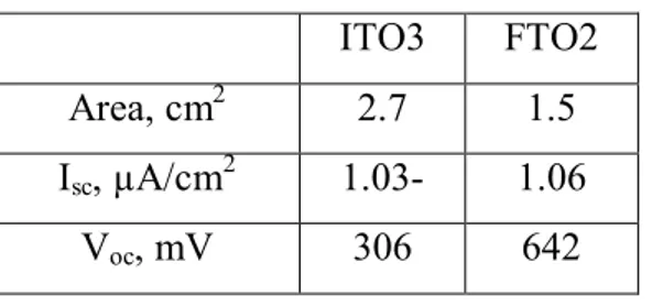
3.3. ITO and FTO electrodes.
We have decided to try to change substrate glass for glass with a more chemically stabilized layer of fluorine-doped tin oxide (FTO). Therewith the electrical conductivity of FTO is higher than electrical conductivity of ITO.
Samples FTO2 and ITO3: mixture №1 (Tab.3.3) was put on the glass by sprayer a few times. First the functional layer was covered with auxiliary layer of P3OT (18
mg/ml), which was made by sprayer too. CVC curves of these samples are on the figure 3.3.1. 0 50 100 150 200 250 300 -3,0 -2,5 -2,0 -1,5 -1,0 -0,5 0,0 V, mV ITO3 I, A 0 100 200 300 400 500 600 700 -1,8 -1,6 -1,4 -1,2 -1,0 -0,8 -0,6 -0,4 -0,2 0,0 0,2 V, mV FTO2 I, A a b
Figure 3.3.1 CVCs of cells with an electrode from glass with layer: a – ITO; b – FTO.
Table 3.3 Result of measurements of CVCs of samples ITO3 and FTO2.
ITO3 FTO2
Area, cm2 2.7 1.5
Isc, µA/cm2 1.03- 1.06
Voc, mV 306 642
As a result these samples have high voltage and higher current than those before. As we predicted, the voltage of the cell with electrode from FTO is higher than the cell with ITO. It is more expedient to use FTO in the future.
3.4. Changing of dye. Molecule-bridge – PyreneMethanol.
We try to change dye PM for another dye N3 (fig.3.4.1a). This dye N3 has a much wider spectrum of absorption than dye N-(1-pyrenyl)maleimide (fig.3.4.2). In this case we have some problems because NT is inert and it is not possible to connect it with ruthenium dye. We can use molecules with pyrenil group for stacking to NT and OH group for interaction with dye – the molecule-bridge which is PyreneMethanol (PMt) (fig.3.4.1b). The iodine liquid electrolyte was used as redox system for this type of cells.
a b
Figure 3.4.1 Chemical structure of dyes: a – N3 [2]; b – PyreneMethanol.
a b
Figure 3.4.2 Absorption spectra of dyes: a - N3 [3]; b – PM [4].
Three solutions were prepared for fabrication of cells:
1. Suspension of SWNTs in ethanol solution of Pyrenemethanol (1mg/1mL) 2. Solution of dye N3 in ethanol (1.35x10⁻⁴M)
3. Liquid electrolyte I2/I3- in polar solvent propylene carbonate (0.5M LiI, 0.005M I2).
Then we are used different methods of the deposition of the functional layer of NTs to form the experimental cell. It is described in the next paragraph.
3.4.1. Comparison of methods of the deposition and of variations of the composition in suspension.
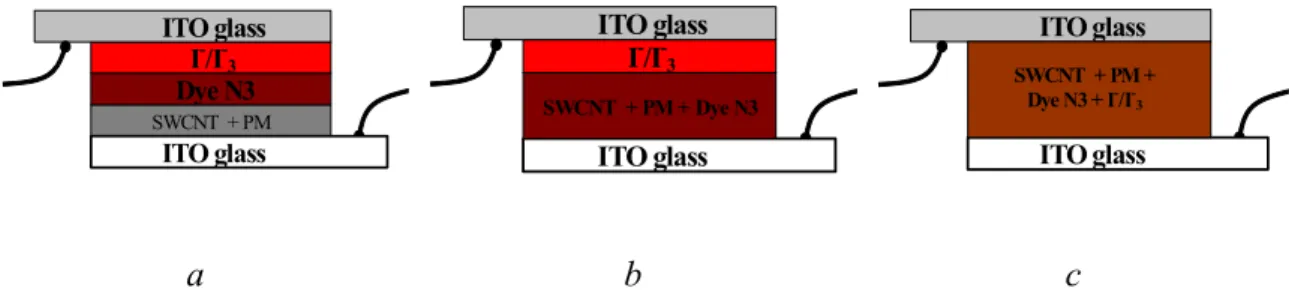
For the first step two lines of samples were prepared: 1 – deposition by spin coating; 2- deposition by evaporation of solvent. Every line has three types of samples with different architecture (fig.3.4.3). Type 1 - every layer of components are sequentially placed on the substrate from its solutions: SWNT with attached PM molecule, dye N3, then the iodine electrolyte and ITO electrode (samples I.3.1. and I.4.1.). Type 2 – the first layer on the substrate is from a solution including SWNT-PM and dye N3 together, then the iodine electrolyte and ITO electrode (samples I.2.1. and I.2.2.). Type 3 – it has only one layer from solution including all components (sample I.1.1.). SWCNT + Dye N3 SWCNT + PM ITO glass I-/I-3 ITO glass Dye N3 SWCNT + Dye N3 ITO glass I-/I-3 ITO glass SWCNT + PM +Dye N3 SWCNT + Dye N3 ITO glass ITO glass SWCNT + PM + Dye N3 + I-/I -3 a b c
Figure 3.4.3 a – architecture of cell of type 1; b – architecture of cell of type 2; c –
architecture of cell of type 3.
Below the result of CVC measurements is showed as the diagram (fig. 3.4.4). positive result null resalt I.1.1. 0,3 A 3,5 mV I.2.2. 0,4 A 20 mV I.4.1. 1 A 32 mV spin coating evaporation NT+dye+ electrolyte NT+dye NT Method of putting composition of suspension for first laeyr of cell
Fifure 3.4.4 Diagram of result of the combinations of method of deposition of every
The sample I.3.1. is the same as I.4.1., the only difference is the temperature of evaporation, but the CVCs are completely different. I.3.1. sample don’t has nothing photovoltaic effect (fig.3.4.5).
-200 -100 0 100 -0,04 -0,02 0,00 0,02 0,04 I, A V, mV 0 10 20 30 -1,0 -0,8 -0,6 -0,4 -0,2 0,0 V, mV I, A a b
Figure 3.4.5 CVCs of cells I.3.1 (a) and I.4.1 (b).
While the evaporation for I.3.1 thermal mass movement was observed of the solvent generating the chaotic motion of NTs in the drop and their subsequent collision and conglomeration. Thereby, film is not formed on the glass surface, but is an array of large conglomerates, easily visible by eye. Working surface of the sample has large areas of bare electrode, and the cell doesn’t have any photoelectric effect. Temperature of heating was not controlled in a special way, and the heater has an error of not less than 15 oC. Thus, the temperature of evaporation of the solvent could be close to the boiling point of ethanol (78 oC), it can activate diffusive motion of NT. To reduce the observed effects of conglomeration, we lowered the evaporation temperature (<50 oC) and the concentration of NT (about 0.3 mg / mL) - sample I.4.1. This sample has a short-circuit current about 1 µA and open-circuit voltage 32 mV. Accordingly, the spatial separation of functional layers for the sample was done.
-20 -15 -10 -5 0 5 10 15 20 -0,03 -0,02 -0,01 0,00 0,01 0,02 0,03 I, A V, mV 0 5 10 15 20 -0,3 -0,2 -0,1 0,0 I, A V, mV A b
Figure 3.4.6 CVCs of cells I.2.1 (a) and I.2.2 (b).
I.2.1 sample was second type the architecture of the cell, it was created by spin coating. The results of CVC measurement confirms that the spin coating did not create the necessary functional film on the ITO glass (fig.3.4.6a). In the case of I.2.1 sample dye N3 is in the basic suspension, and was not added again by evaporation in the refrigerator. As a result, the photoelectric effect isn’t even. For I.2.2 sample, we can see a photoeffect (short-circuit current 0.4 μA/cm2, open-circuit voltage 20 mV) (fig.3.4.6b). Current and voltage for this sample is lower than for the sample with a separate layer of NT and layer of dye N3 (I.4.1). This can be explained by the fact that the sample I.4.1 has its first layer of clear metal NT and it formed an upper layer of dye, which generates charge carriers. Then carriers are separated by "heterostrucrure" NT-dye-electrolyte. The dye layer is very thin, almost monomolecular in this case. Free dye molecules were removed by washing them in the solvent. In the case I.2.1, dye molecules were already in suspension, and after evaporation, they formed a layer between the nanotubes. These layers hinder transfer and charge separation, carriers can’t pass through a lot molecules of dye.
I.1.1 sample has the photoelectric effect (fig.3.4.7). The viscosity of the liquid electrolyte has helped create a more uniform film. However, the CVC has jumps and dips, the voltage are very low. All of this is caused due to the geometrical and electrical disorder of the system. Carriers, after absorption of light, recombine in the near electrolyte, and a complete charge separation does not occur. We were unable to make I.1.2 sample.
-0,5 0,0 0,5 1,0 1,5 2,0 2,5 3,0 3,5 4,0 -0,30 -0,25 -0,20 -0,15 -0,10 -0,05 0,00 0,05 I, A V, mV
Figure 3.4.7 CVCs of cells I.1.1.
3.4.2 Comparison of different electrodes.
We have considered different kinds of electrodes, that is substrate for deposition of the functional layer: glass with indium tin oxide (ITO), glass with fluorine tin oxide (FTO); the electrode of ITO glass with a layer of aluminium on the top; FTO glass with a thin layer of colloidal graphite. The results of photovoltaic measurements are in table 3.4.
Table 3.4 Data of samples.
Name of sample Electrode Isc, μA/cm2
Voc, V
Dark7 Glass FTO 18 0,131
Dark4 Glass ITO - -
ITOAl Glass ITO + Al 1 0,600
Graph1 Glass FTO + graphite 1,5 0,356
In our system, solar cells contain liquid electrolyte iodine; iodine is a corrosive medium for other parts of cells. The liquid electrolyte can penetrate between the nanotubes up to the opposite contact. The sample Graph1 was covered with a layer of colloidal graphite for obstruction of electrode with the nanotubes from electrolyte. In this case the thickness of the sample increased and therefore open-voltage increased too, but impurities of the graphite in network of nanotubes prevents the electron current.
Aluminium layer was coated upon the ITO glass in the ITOAl sample. In this metal-metal contact a contact electric field may be generated from differences in the work functions of metals. This field may exceed the spatial border of metals. It may affect the NT and pull the current charge from NT. As a result, the short-circuit current of this sample is as low as before, and the system is not justified.
For a Dark4 sample with electrodes from glass ITO failed to get a successful CVC. Perhaps the film of NT had a lot of cracks and there was a short circuit made by liquid electrolyte.
The Dark7 sample demonstrates the better result; it has electrodes from glass with FTO. Open-voltage of this sample is not as high, but then we chose current as a more important parameter. Current is higher by 18 times, and the voltage is lower by 4.5 times, and fluorine is more resistant to the corrosive medium of iodine in comparison with indium. Finally, we chose an electrode with a glass of FTO for future research.
3.4.3. The dimension of the sample.
A diffuse movement of NT in a drop and their conglomeration accompanies the evaporation of the solvent, when we have clusters of NT and the voids between them on the electrode. Also the drop of suspension on the substrate has heterogeneity of the thickness because there is surface tension of the solvent, finally we have gradient film thickness. Probably a decrease in the sample area will help improve the uniformity of the film.
Comparison of the current-voltage characteristics of samples with different area was realized. Samples (type 1) were prepared on the glass with FTO: a layer of SWNT-OH + dye N3 - 2 times by evaporation at 50 ° C, a layer of N3 - 1 times by evaporation at 50 ° C, the liquid electrolyte I2/I3-. The second electrode was glass with FTO. The results of photovoltaic measurements are on table 3.5.
Table 3.5 Data of samples.
Name of sample S, cm2 Isc, μA/cm2
Voc, V
Dark5 0.5 5 0,247
Dark1 0.09 33 0,242
Dark2 0.04 33 0.177
From the data on table 3.5 we see, that the samples with low areas 0.09 and 0.04 cm2 characterized by a high short-current circuit. Also, the CVC curve of the sample with an area of 0.5 cm2 has many dips (fig.3.4.8b). Increasing the sample size led to an increase in the number of hollow space and pinholes into the film, because of which a point short-circuit, occur in the sample, this causes jumps and peaks in the CVC (fig.3.4.8). Instability of CVC of previous samples were induced by the penetration of liquid electrolyte into the pores of the film.
-20 0 20 40 60 80 100 120 140 160 180 200 -1,4 -1,2 -1,0 -0,8 -0,6 -0,4 -0,2 0,0 V, mV I, A 0 50 100 150 200 -4,0 -3,5 -3,0 -2,5 -2,0 -1,5 -1,0 -0,5 0,0 V, mV I, A a b
Figure 3.4.8 CVC of Dark2 sample (a). CVC of Dark5 sample (b).
3.4.4. Amount of the functional layer on the electrode.
To study the influence of the thickness of functional layer to the CVC, samples were prepared with different numbers of layer on the substrate. All samples have an area of 0.09 cm2 and deposited from suspension SWNT-OH + dye N3. The results of photovoltaic measurements of these samples are in table 3.6 and on the figure 3.4.9.
Table 3.6 Data of samples.
Name of sample Number of layers I, μA/cm2 V, V
Dark1 2 33 0.242 N3 4 24 0.320 N5 6 14 0.475 N4 8 3 0.606 1 2 3 4 5 6 7 8 9 0 5 10 15 20 25 30 35 Isc, A N 2 3 4 5 6 7 8 0,20 0,25 0,30 0,35 0,40 0,45 0,50 0,55 0,60 0,65 Voc, Volt Number of layers a b
Figure 3.4.9 a - the short-circuit current on the number of layers (film thickness), b -
the open circuit voltage on the number of layers.
These characteristics of graphics were expected. With increasing thickness of film open-voltage, respectively also increases, U~d. Current falls, as the increased number of centres of relaxation, in which the excited carriers relax before arriving to the electrodes of the cell. The film thickness inversely affects the current charges. In thicker films there are more different kinds of defects, in which the charge carriers recombine. Photons are absorbed by the upper layers and do not reach the others, the diffusion length of carriers is less than the thickness of the film, and some carriers lose their energy before reaching the opposite electrode and others reach it with very low stored energy.
There are reflectance and scattering spectrums of films: anatase TiO2, dye N3 and SWNT-OH to determine the role of the nanotubes in the absorption of light (fig.3.4.10).
a b Figure 3.4.10 a - reflectance spectrum, b - scattering spectrum.
From the above spectra, we can estimate that the SWNT-OH in the wavelength before 550 nm mainly absorbs light. Colour film SWNT-OH is black, so the share of transmission is very small and most part of the light is absorbed. The absorption is comparable with the absorption of the dye N3, and the photocurrent of SWNT is very low (fig.3.4.11a square).
Figure 3.4.11 The current of the devise vs time with different optical intensities (VSD = 3 V and I from 50 to 200 mW/cm-2) (a). The band line up of currents vs time with various optical intensities (b). [SWNTs (■); V-SWNTs (●); and Ru-3/V-SWNT (▲)]. [5].
The low value of current in our cells could be explained by the fact that most of the photons of radiation absorbed by the nanotubes, so photons pass in small number to excite photocarriers in the dye layer.
REFERENCES
1. S. Bhattacharyya, E. Kymakis, and G. A. J. Amaratunga. Chemistry of Materials. 2004, 16, pp. 4819-4823.
2. K. Kalyanasundaram, M. Grätzel. Material Matters. Aldrich Chemical. 2009, 4(4), pp. 88-91.
3. L.C.T. Shoute, G.R. Loppnow. Journal of the American Chemical Society. 2003, 125 (50), pp. 15637 15646.
4. J. Li, D.J. Bigelow. Biochemistry. 2003, 42, pp. 10674-10682.
5. W. Lee, G. Koo et al. The Journal of Physical Chemistry C.. 2009, 113, pp. 13403– 13408.
CHAPTER IV
EXPERIMENTAL PART AND DATA DISCUSSION ELECTROPHORESIS
The next step of our work main aim was to work out easy and economic method of the formation of uniform NT layer on the large-area. For it we chose the electrophoresis. There are different scientific works about of electrophoresis of SWMTs [1]. Kim and coworkers described vertical alignment of SWCNT film formed by electrophoresis [2], the series of samples was prepared respectively this method.
4.1. Preparation of SWNTs for electrophoresis.
Before SWNTs have to prepare for electrophoresis by special steps. Firstly, we have to cut SWNTs to shorter pieces. SWNTs were shortened by processing using oxidizing acid, sonication (60 kHz) in a mixture of concentrated sulfuric and nitric acids (3:1, 97% and 70%, respectively) at 40°C for 24 hours. The goal herewith the SWNT ropes was not just to damage the tubes but to cutthem cleanly at the points of damage and separate the cut pieces from the other tubes in the ropes. The advantage of sonicatingin the presence of an oxidizing acid is that subsequent attackat the point of damage soon cuts the tube completely. The 3:1 concentrated H2SO4:HNO3 mixture was chosen for the oxidizing acid in this cutting operation because it is also known to intercalate and exfoliate graphite. From literature we found that in 3:1 concentrated sulfuric and nitric acid at 70°C the average cut nanotube shortened at a rate of roughly 130 nmhour 1. next we had to wash SWNTs. Washing was ten times in distilled water with centrifugation at 5 С at 4500 rpm for 2 hours for every time, then it was evaporation of liquids at 90 С for 24 hours. After it was washing again at 5 С at16000 rpm for 40 min. Next was total evaporation of liquids at 50 oC for 10 days. The residual of SWNTs was 0,04 g.
The collected SWNTs after were immersed into SOCl2 for 24 h to convert the carboxylic acid groups into the corresponding acyl chloride. After completion of the reaction, the black SWNTs-COCl suspension was centrifuged at 4500 rpm for a few
hours to eliminate remaining byproducts, and then diluted with dimethylformamide (DMF, 0.001% water). After repeating the process a few times, we obtained the SWNTs-COCl/DMF solution with a small amount of byproducts.
4.2. Process of electrophoresis. The fabrication of the cell.
For electrophoresis it were used constant-current source ISA JOBIN YVON ALIMENTATION P.M. 2000 and two electrodes from glass with ITO layer (1x5 cm) in plastic cubic cell (1x1x4 cm). The spacer between electrodes was teflon 8mm. The electrophoresis was applied by 150 V for 10 min (fig.1).
a b c d
Figure 4.2.1 Process of electrophoresis. The time of process, min: a – 0; b – 1; c – 5; d
– 10.
The electrode with SWNTs was used for fabrication of cell. The layer of NT was covered with dye N3 by evaporation fron the solution ethanol (1.35x10⁻⁴M). Then it was closed with second electrode and fulled of liquid iodine electrolyte. The schematic architecture is showed on the figure 422.
SWCNT deposited by electrophoresis
I
-/ I
3-Glass ITO
Glass ITO
Layer of dye N34.3. Current-Voltage Characteristics. SEM measurements.
A series of samples were prepared with different concentration of SWNTs in suspension for electrophoresis. Concentration were, mg/mL: 0.02; 0.006; 0.003; 0.002. SEM measurements of face and of profile were realized for every sample (fig.4.3.1).
a
b
Figure 4.3.1 SEM images of the sample with concentration 0,002 mg/mL. a – plan
view; b – profile.
The dependence of the thickness of SWNT film and the dependence of the diameter of Nt bundles on the concentration of NT in suspension for electrophoresis were determined by SEM data. Diameter of bundles and thickness of film increase with the concentration as expected (fig.4.3.2)
0,000 0,005 0,010 0,015 0,020 1,99 2,00 0 200 400 600 800 2800 3000 Concentration of SWNT, mg/mL Thickness, nm 0,000 0,005 0,010 0,015 0,020 0,025 10 20 30 40 50 60 70 80 90 Concentration of SWNT, mg/mL Dparticles, nm a b
Figure 4.3.2 The dependence of the thickness of SWNT film (a) and the dependence of
the diameter of NT bundles (b) on the concentration of NT in suspension for electrophoresis.
NT bundles had diameter of tens of nanometers, it means that bundles was formed from tens of SWNT. The bundle was a net of NTs. And if a bundle has vertical alignment when NTs of bundle can be disorientate. We think that after preparation of SWNTs for electrophoresis SWNTs was cut too much. It is possible that NTs was cut to a very short length, so bundle was formed from not aligned NT pieces.
The photovoltaic cell was fabricated samples of electroforesis in compliance with the architecture of cell showed on the figure 4.2.2. Cells of electrophoresis don’t show improvement of values of the short-current and of the open-voltage but these cells have improvement for fill factor of the cell (fig.4.3.3).
-25 0 25 50 75 100 125 150 -1,8 -1,6 -1,4 -1,2 -1,0 -0,8 -0,6 -0,4 -0,2 0,0 V, mV N9 I, A/cm2 0 100 200 300 400 500 600 700 -0,5 -0,4 -0,3 -0,2 -0,1 0,0 V, mV I, A N4 a b
Figure 4.3.3. a – CVC of the cell based on the sample of electrophoresis; b – CVC of
The fill factor is defined as the ratio of the actual maximum obtainable power to the product of the open-voltage and short-circuit current:
OC SC MP MP T MAX
V
I
V
I
P
P
FF
(4)The fill factor of solar cell of formerly was about 0.4 – 0.5, for cells of electrophoresis it was about 0.7 – 0.75, that is the fill factor for typical commercial solar cells.
The method of formation of SWNT layer give the possibility to create the large-area samples with uniform film of NT and improve the cell’s properties.
REFERENCES
1. V. P. Kamat, K. G. Thomas. Journal of the American Chemical Society. 2004, 126, pp. 10757-10762.
CHAPTER V
EXPERIMENTAL PART AND DATA DISCUSSION METAL-ORGANIC CHEMICAL VAPOR DEPOSITION
5.1. Formation of nanostructured composition materials based on Multi-walled Carbon Nanotubes by Metal-Organic Chemical Vapor Deposition. Synthesis.
MOCVD plant (metal-organic chemical vapor deposition) was used for fabrication of the macrocylinder with constant thickness of the wall created from radially oriented multi-walled carbon nanotubes (MWNT), the scheme of the plant is showed on the figure 5.1.1 There is a tubular quartz reactor of the turning type (length - 600 mm, diameter - 25 mm, and the double-step system of the heating furnaces [1].
Figure 5.1.1. Scheme of MOCVD plant for fabrication of the macrocylinders with
constant thickness of the wall created from radially oriented MWNT. 1 – flowmeter AALBORGGFC17; 2 – argon; 3 – stopcock; 4 – toluene; 5 – bypass; 6 – thermometer HANNA HI93530; 7 – furnace of the evaporation; 8 – ferrocene Fe(C5H5)2; 9 – autotransformer; 10 – furnace of the reaction; 11 – substrate; 12 – waterlock.
The synthesis of macrocylinders with constant thickness of wall was in the argon flow at atmospheric pressure. Velocity of the argon flow was regulated by the high-precision flowmeter AALBORG GFS17. The argon was passed to the bubbler filled toluene. Toluene vapor moved by argon flow was passed to quartz reactor with double-step system of the heating furnaces. Figure 5.1.2 shows the curve of distribution
of the temperature depending on point of the reaction furnace. The central part of furnace has the distance about 5 cm of constant temperature (Fig5.1.2). Macrocylinders of MWNT were deposited to cylindrical quartz substrate with length of 5 cm and diameter of 17 mm at temperature of 850 oС at the central point of the furnace.
Figure 5.1.2. Distribution of the temperature depending on point of the reaction
furnace.
Ferrocene in the furnace of evaporation at temperature 100 - 105 oС was evaporated and was moved with toluene vapor by the argon flow to the hot part of the second furnace. Therefore the pyrolysis of ferrocene and of toluene occurred gererating the growth of MWTNs. The thermal decomposition of ferrocene vapor produces iron nanoparticles on the cylindrical quartz substrate and there is future growth of MWNTS. On figure 5.1.3 there is photo of microcylinder formed by 7 hours.
Figure 5.1.3. Photo of macrocylinder with constant thickness of the wall from radially
oriented multi-walled carbon nanotubes.
A study of morphology of cylinders was exercised by scanning electron microscope Supra 50 VP (Zeiss) and by transmission electron microscope JEM-2010: an accelerating voltage was 200 kilovolt, resolution was 0.14 nm. SEM images of cylinder are on the figure 5.1.4a, b, c. From SEM images we can observe, that walls of
macrocylinder have radially oriented multi-walled carbon nanotubes and bulk of them. Also we can notice, that a space is between bulks, whith can be filled within. Observed NTs were as the thick (diameter about 100 nm) as the thin (diameter about 20 nm) MWNT, most part them were closed [2]. Four different structural parts of the cross-section of cylinders were indicated by SEM study 5.1.4d.
a b
c d
Figure 5.1.4. a, b, c – SEM images of cylindrical section. d – Schema of the structure
of the cross-section of the macrocylinder. 1 – part of the contact between mass of MWNT and quartz substrate, part of chaotic growing; 2 – wavy part; 3 – main part of the growing of radially oriented MWNTs; 4 – interior part of the macrocylinder formed bulks of MWNTs.
Samples for fabrication solar cell based on the mass of aligned CNT were created by this MOCVD method. We used two type of quartz substrate: cylindrical and flat. The principle of flat growing is same cylindrical growing.
5.2. Flat MOCVD samples with MWNTs. Thickness. Absorption.
Flat samples grew by MOCVD method were the flat quartz substrate with film of perpendicularly oriented aligned multi-walled carbon nanotubes, which can be used for fabrication of solar cell. A study of the thickness of the film of NTs, depending on the weight of the film of NTs, consequently on growth parameters.
Table 5.2.1. Data of MOCVD flat samples.
N of sample Layer of nickel Weight of MWCNT, mg Thickness of MWCNT layer, µm E-11-122 - 1.50 - E-11-123 - 1.25 - E-11-124 + 3.65 200 ± 20 E-11-125 + 1.25 50 ± 10 E-11-126 + 0.1 10 ± 4 E-11-127 + 0.3 30 ± 4 E-11-128 - 1.5 80 ± 20 E-11-129 - 0.1 10 ± 4 E-11-132 + <0.1
Samples of the flat layer of MWNTs on the quartz substrate 1x2 cm2, some samples have the nickel layer between quartz and MWNT (“+” in Tabl.5.2.1 means the presence of nickel layer). The nickel layer was deposited on the quartz substrate by plasma spraying before of synthesis of MWNTs. The resistivity of the nickel layer is 57712 ohm-cm and the spectrum of transmission is on the figure 5.2.1. where the nickel layer was used as the starting layer to grow of MWNTs and as the electrode - for future cell. The transmission of quartz substrate with a nickel is decreased, but it has sufficient value for using it in order to create the cell.
Figure 5.2.1. Transmission spectrum of nickel layer on the quartz substrate. Thickness
of nickel layer, nm: 1 – 15; 2 – 30.
The difference of the quantity of MWNTs can be seen by the nakel eye (fig.5.2.2). The thickness of MWNT layer depend on the weight of NTs as we show on figure 5.2.3a, the dependence of the absorption spectrum on the weight is shown on figure 5.2.3b.
a b c d
Figure 5.2.2. Photo of flat MWNT samples grew by MOCVD. Weight of the MWNT
film on the quartz substrate, mg: a – 0.1; b – 0.3; c – 1.25; d – 3.65.
0,0 0,5 1,0 1,5 2,0 2,5 3,0 3,5 4,0 0 40 80 120 160 200 240 T h ic k n e s s , m weight of MWNT film, mg 300 450 600 750 900 0 1 2 3 4 5 4 3 2 mass of MWNT: wavelength, nm a b s o rb a n c e 1 a b
Figure 5.2.3 a – dependence of the thickness of MWNT layer on the weight of
MWNTs; b – absorption spectrums of MWNT film by weight of the film, mg: 1 – 0.1; 2 – 0.3; 3 – 1.25; 4 – 3.65.
The layer with a thickness of about 200 µm is a very thick and black, it absorbs the full-spectrum light. In spectrums peaks of 350 nm, 380 nm, 420 nm, 450, 680 nm are peaks of the quartz substrate. In figure 3.2.3b on lines 3 and 4, it was taken into account, but was not taken into account for lines 1 and 2.
SEM images of the most lightweight samples E-11-132 is showed below (fig.5.2.4).
a b
Figure 5.2.4. SEM images of E-11-132 samples.
On SEM images we can observe that the MWNT layer on the flat quartz substrate is formed from the buffer layer of carbon nanoparticles and a growing straight up bulk of MWNTs on the top. It isn’t an aligned layer of NTs as in case of cylindrical substrate, but there are the uniform, homogeneous, continuous layer of MWNTs.
![Figure 2.3.2 Absorptions of dyes: a - N3 [36]; b – PM [37].](https://thumb-eu.123doks.com/thumbv2/123dokorg/2870553.9386/21.892.183.738.196.479/figure-absorptions-dyes-n-b-pm.webp)
![Figure 3.4.2 Absorption spectra of dyes: a - N3 [3]; b – PM [4].](https://thumb-eu.123doks.com/thumbv2/123dokorg/2870553.9386/32.892.208.722.389.646/figure-absorption-spectra-of-dyes-a-n-pm.webp)