Reconfiguration for Hardware-Software Co-Design in FPGA SoC
Biruk Seyoum
biruk.seyoum@ santannapisa.it TeCIP Institute, Scuola
Superiore Sant’Anna Pisa, Italy
Marco Pagani
marco.pagani@ santannapisa.it TeCIP Institute, Scuola
Superiore Sant’Anna Pisa, Italy
Alessandro Biondi
∗alessandro.biondi@ santannapisa.it TeCIP Institute, Scuola
Superiore Sant’Anna, Pisa, Italy
Giorgio Buttazzo
∗giorgio.buttazzo@ santannapisa.it TeCIP Institute, Scuola
Superiore Sant’Anna, Pisa, Italy
ABSTRACT
Despite its benefits, hardware acceleration under dynamic partial reconfiguration (DPR) has not been fully leveraged by many sys-tem designers, mostly due to the complexities of the DPR design flow and the lack of efficient design tools to automate the design process. Furthermore, making such a design approach suitable for real-time embedded systems requires the need for extending the standard DPR design flow with additional design steps, which have to accurately account for the timing behavior of the software and hardware components of the design, as well as of the components of the computing platform (e.g., the reconfiguration interface).
To address this problem, this paper presents DART, a tool that fully automates the design flow in a real-time DPR-based system that comprises both software and hardware components. The tool targets the Zynq 7-series and Ultrascale+ FPGA-based SoCs by Xilinx. It aims at alleviating the manual effort required by state-of-the-art tools while not expecting high expertise in the design of programmable logic components under DPR. To this purpose, it fully automates the partitioning, floorplanning, and implementa-tion (routing and bitstream generaimplementa-tion) phases, generating a set of bitstreams starting from a set of tasks annotated with high-level timing requirements. The tool leverages mathematical optimization to solve the partitioning and floorplanning problems, and relies on a set of auto-generated scripts that interact with the vendor tools to mobilize the synthesis and implementation stages. DART has been experimentally evaluated with a case study application from an accelerated image processing system.
KEYWORDS
FPGA SoCs, Dynamic Partial Reconfiguration, Design Automation
ACM Reference Format:
Biruk Seyoum, Marco Pagani, Alessandro Biondi, and Giorgio Buttazzo. 2021. Automating the Design Flow under Dynamic Partial Reconfiguration for Hardware-Software Co-Design in FPGA SoC. In The 36th ACM/SIGAPP ∗Also with the Department of Excellence in Robotics & AI, Scuola Superiore Sant’Anna.
Permission to make digital or hard copies of all or part of this work for personal or classroom use is granted without fee provided that copies are not made or distributed for profit or commercial advantage and that copies bear this notice and the full citation on the first page. Copyrights for components of this work owned by others than ACM must be honored. Abstracting with credit is permitted. To copy otherwise, or republish, to post on servers or to redistribute to lists, requires prior specific permission and/or a fee. Request permissions from [email protected].
SAC ’21, March 22–26, 2021, Virtual Event, Republic of Korea © 2021 Association for Computing Machinery.
ACM ISBN 978-1-4503-8104-8/21/03. . . $15.00 https://doi.org/10.1145/3412841.3441928
Symposium on Applied Computing (SAC ’21), March 22–26, 2021, Virtual Event, Republic of Korea. ACM, New York, NY, USA, Article 4, 10 pages. https://doi.org/10.1145/3412841.3441928
1
INTRODUCTION
In the context of safety-critical systems, FPGA-based system-on-chip (SoC) platforms are a particularly attractive solution. Com-pared to other types of hardware acceleration, such as GPU co-processing, FPGA-based acceleration allows for a fine-grained con-trol of the logic design, resulting in a very flexible and time-predictable type of acceleration. This characteristic is crucial for allowing an accurate estimation of the worst-case execution times (WCET). Fur-thermore, the dynamic partial reconfiguration (DPR) capabilities of modern FPGA-based SoC platforms can be leveraged to improve resource utilization, resulting in lower requirements in terms of FPGA resources compared to a static approach. In addition to the improvement in resource utilization, the increasingly lower FPGA reconfiguration time makes these platforms particularly interest-ing in the context of real-time systems, which typically consist of periodic or sporadic computational activities [3].
A typical co-design flow for implementing a real-time system on a DPR-enabled FPGA-based SoC platform begins by classifying the ensemble of activities performed by the system into (i) software tasks (SW-tasks), which are regular software activities executed on the CPUs available on the SoC, and (ii) hardware tasks (HW-tasks), which are hardware description language (HDL) implementations of computationally-intensive functions to be offloaded on the FPGA. Under DPR, HW-tasks can be logically partitioned and assigned to one or more reconfigurable regions (RRs) defined in the total FPGA area. Such a partitioning phase is an important design step in the DPR design flow as it has the potential to determine both the FPGA resource consumption and performance of the system. For instance, if two hardware tasks are partitioned on the same RR, then the RR must contain enough FPGA resources to host both of them in mutual exclusion, hence requiring the maximum of the FPGA resources requested by each hardware task for each resource type (CLB, DRAM, DSP). At the same time, the two hardware tasks must be capable of tolerating the delays that can be originated due to contention of the RR, i.e., in the worst case, one of the two must wait for the entire time the other occupies the RR before being able to be dynamically configured on it.
The partitioning design step is followed by the floorplanning phase, which geometrically maps the RRs on the physical FPGA fabric, which is known to be a non-trivial task due to the vast design space to be explored. The last design steps in a DPR design
flow are the implementation (placement and routing) and bitstream generation phases. These design stages are usually automated by the vendor design tools, but can sometimes require manual intervention to some extent. At the completion of the design flow, full and partial bitstreams are generated.
These issues constitute a barrier to unlock the potential of FPGA-based acceleration under DPR and we attribute them to the manual steps involved in the flow. Despite the benefits introduced by DPR-based hardware acceleration for real-time systems, performing a DPR design flow is a tedious and time-consuming process. Devel-opers are required to be familiar with low-level hardware details while, at the same time, taking into account the timing require-ments of the application. The need to follow such a multifaceted approach can hinder software-oriented developers from leveraging the benefits provided by DPR.
Existing commercial DPR design tools partially/fully automate some of the individual design steps, but manual effort is still re-quired to perform the full design flow, which also calls for consid-erable expertise with the technology and tools. Therefore, to date and to the best of our records, the lack of efficient design tools to fully automate the DPR design flow is a key problem to solve to push for a wider adoption of DPR-based hardware acceleration. Contribution. The purpose of this paper is to meet the aforemen-tioned demand by presenting DART (Design Automation for partial Reconfiguration Tool), a tool that fully automates the design flow for hardware-accelerated real-time systems on DPR-enabled, FPGA-based SoC platforms. DART inputs the implementations of the HW-tasks, the timing requirements of the SW-tasks and HW-tasks, and the type of FPGA, and generates as output the full and partial bitstreams of the design without requiring any intervention from the designer.
DART advances the state of the art as follow:
• It combines the DPR partitioning and floorplanning prob-lems into a single optimization problem and solves it us-ing a holistic objective mixed integer linear programmus-ing (MILP) optimization. Despite the partitioning and floorplan-ning have been independently solved in the past using MILP optimization based approaches [4, 12], combining them into a single optimization problem is the unique way to guarantee globally optimal solutions.
• It fully automates the placement, routing, and bitstream generation design steps in the DPR design flow by utilizing a set of auto-generated Tcl scripts that interact with, and command, the vendor design tools. To further support the designer, DART also includes a diagnostic stage to fix errors and rerun the design in case of an error at the implementation (routing and bitstream generation) stage.
The performance of DART was finally evaluated by automating the design flow of a DPR-based image processing system on a PYNQ-Z1 platform.
2
BACKGROUND AND MODELING
This section describes the software programming model, the design steps in a DPR flow, and the corresponding models adopted in this paper. This work is based on the 7-series and Zynq UltraScale+ SoC
families from Xilinx and builds upon a series of previous works, which are reviewed in the following sections.
2.1
Programming model
In a typical DPR-based hardware-software co-design approach, the execution of HW-tasks on the FPGA is invoked by acceleration re-quests issued by SW-tasks. If the HW-task of interest is not statically allocated on the FPGA area, the acceleration request is followed by a runtime partial-reconfiguration (dynamic loading) of the re-quested reconfigurable hardware module (RM) that implements the HW-task, which is hosted by predefined reconfigurable region (RR) on the FPGA. Following the framework proposed in [3], the accel-eration requests issued by SW-tasks are blocking, meaning that the SW-task that requested the acceleration will remain suspended (i.e., it will release the CPU on which it is executing) until the requested hardware accelerator finishes execution. Following the typical task-based paradigms adopted in real-time systems, theithSW-task is periodically activated with a periodTi, i.e., it repeats a certain com-putation everyTitime units, and is subject to a relative deadline Di, meaning that it must complete its execution withinDi units of time from its activation.
As an example, consider the timing diagram reported in Fig-ure 1, which depicts the execution of DPR-based application. The application contains three SW-tasks, namelysw1,sw2, andsw3, and four HW-tasks (each corresponding to an RM) allocated in two RRs. The first two RMs,RM1 andRM2, are allocated to the first reconfigurable region,RR_1, while the last two RMs, RM3andRM4, are allocated to the second reconfigurable regionRR_2. Note that two acceleration requests for different RMs allocated to the same RR can cause interference both at the reconfiguration interface and at the RR (e.g., see the 1stand 2ndacceleration requests in Figure 1). Conversely, acceleration requests for RMs allocated to different RRs can incur interference only at the reconfiguration port (e.g., see the 1stand 3rdacceleration requests in Figure 1).
To manage the contention at the FPGA reconfiguration port (ICAP, PCAP, SelectMAP, etc.) and at the RRs, the scheduling in-frastructure proposed in [3] is used, which consists of a multi-level queuing mechanism. Under such a scheduling mechanism, the de-lays incurred by HW-task requests are bounded and predictable1.
2.2
The DPR design flow
This work focuses on the DPR design flow for Xilinx platforms, which is illustrated in Figure 2. The design flow includes four major design steps, namely (i) partitioning, (ii) floorplanning, (iii) static part generation, and (iv) routing and bitstream generation. (i) Partitioning: In this step of the design flow, the set of HW-tasks (each corresponding to an RM) is partitioned and allocated into distinct RRs on the FPGA fabric. Each RR can host more than one RMs, which will be executed in a time-multiplexed manner. The considered applications have a total numberNsw andNhwof SW-tasks and HW-SW-tasks, respectively. TheNhwHW-tasks are hosted onNRRFPGA reconfigurable regions (RRs), whereNRR ≤Nhw. The RMs are allocated to RRs either in a "many to one" or "one to one" mode and no RM can be allocated to more than one RR. The
Reconfig. port RR_1 SW_1 SW_2 Suspension SW_3 RR_2 RM1 RM2 RM1 RM3 RM4 1 2 3 4 5 Task
activation Accelerationrequest
Deadline Suspension HW acceleration precedence N
Figure 1: An example of real-time DPR acceleration on FPGA-based SoC with 3 SW-tasks and 4 RMs. The process-ing system of the SoC has 4 processor cores and all SW-tasks run in a different core. RM_1 and RM_2 are allocated to RR_1 while RM_3 and RM_4 are allocated to RR_2.
Logic partitioning
Static part design checkpoint
Partial bistreams Out-of-context synthesis
Floorplanning
Place and route Reconfigurable module HDL sources Bitstreams generation Reconfigurable module HDL sources Full bistreams
Figure 2: Illustration of the Vivado DPR flow. Solid rect-angles denote steps that are automated through scripting, while dashed rectangles indicate manual phases requiring user intervention.
former corresponds to the case in which the RR is managed under DPR, while the latter corresponds to the special case in which an RM is statically allocated to an RR. To mathematically express such an allocation constraint, we defineτij ∈ {0, 1}, a binary variable such thatτij = 1 if and only if the ithRM is allocated to thejthRR, andτij = 0 otherwise. Hence, the constraint that asserts the "many to one" or "one to one" allocation rule can be formulated as follows:
∀i = 1 . . . , Nhw NR R Õ j=1 τi j = 1. (1)
A reconfigurable region (RR) must also satisfy the resource requirements of all the RMs allocated to it. This resource con-straint can be mathematically modeled by defining two param-etersctj ∈ R≥0andαti ∈ R≥0, which respectively denote the num-ber of resources of typet that are available in the jth RR, and
the number of resources of typet required by the ithRM, where t ∈ {CLB, BRAM, DSP}. The above resource constraint can then be formally stated as,
∀j = 1, . . . , NRR,∀t ∈ {CLB, BRAM, DSP}, ∀i = 1, . . . , Nhw cj
t ≥maxi{αti·τij}. (2)
Furthermore, the sum of the resource requirements of all RRs must not exceed the total available resources on the FPGA. Note that, together with the RRs, the FPGA area must also host a static region to implement accessory logic and parts of the system that do not change their functionality at run time. To encode this constraint, we first defineCt ∈ R≥0andSt∈ R≥0to represent the total number of resources of typet in the whole FPGA area and those required by the static region, respectively. Then, this condition can be asserted using the following inequality:
∀t ∈ {CLB, BRAM, DSP} Ct−St ≥ NR R Õ j=1 cj t. (3)
The partitioning of HW-tasks into RRs adopted in this work is based on the timing behavior of both SW-tasks and HW-tasks. For-mally speaking, letΨidenote the maximum interference incurred any acceleration request related to theithRM. Also, letΩibe the FPGA execution time of theithRM andηj be the reconfiguration time of thejthRR. For eachithRM allocated to thejthRR, it must hold that the interferenceΨi, plus the FPGA execution timeΩiand the reconfiguration timeηj must not exceed the maximum time that the SW-task invoking the RM can be suspended without violating its deadline. This is called a deadline-driven timing constraint. The partitioning problem, as considered in this work, is hence charac-terized by a design space exploration to find RM-RR allocations that ensure both the deadline-driven timing constraints and the FPGA resource constraints discussed above. The formulation of the MILP presented in [4] serve this purpose.
(ii) Floorplanning: Floorplanning involves the generation of phys-ical placements for the RRs on the FPGA fabric. The generated FPGA placements (i) must satisfy the resource requirement of the RMs allocated to them, i.e., Equations (2) and (3), (ii) must adhere to the set of technological and structural DPR floorplanning constraints set by the FPGA vendor, and (iii) must not impact the performance of the design, i.e., the placements should not be the cause for a timing violation at the routing stage of the design.
As an example, some of the floorplanning technological con-straints posed by Xilinx include [14]: (i) RRs must not overlap; (ii) RRs must not share tiles in the same clock region; (iii) RRs must be rectangular; and (iv) the left and right vertical boundaries of RRs cannot be placed between back-to-back connected interconnect tiles. In this work, following the approach of [10, 12], the distribu-tion of resources on the FPGA fabric is modeled using a discrete Cartesian coordinate system whose origin is located at the bottom-left corner of the fabric, as shown in Figure 4(a). Each unit on the x-axis denotes a column of a single type of resource (CLB, BRAM, DSP), while each unit on the y-axis represents a clock region. De-pending on the family type, the FPGA fabric is also characterized by columns, which contain non-partially-reconfigurable resources such as the PLLs, ICAP, clock buffers, etc., and are referred to as
forbidden regions. The placement of thejthRR is characterized by the tuple (xj,yj, wj, hj), wherexjandyjrepresent the bottom-left coordinates, andwj ≥ 1 andhj ≥ 1 represent the width and height of the RR, respectively. Note that, such a lower bound for the width and height implies a finegranularity of RRs as low as one column wide and one clock region high. If the total FPGA area isW columns wide andH clock regions high, then the RR placements must respect the following structural constraints:
∀j = 1, . . . , NRR, xj+ wj ≤W ∧ yj+ hj ≤H (4) In Xilinx FPGAs, vertically stacked clock regions usually contain a uniform resource distribution layout. In fact, as demonstrated in Figure 4(a), the resource layout in all the clock regions of the FPGA can be described by using the resource layout in only a single clock region and all the forbidden regions on the fabric. By taking advantage of such a simplified approach for describing the full layout of resources in Xilinx FPGAs, the authors in [12] proposed a resource finger-printing model to analytically define the number of resources of typet in the jthRR, i.e.,ctj. Accordingly, the resource finger-printing model involves the encoding of the distribution of resources of typet found in the first clock region only, which is accomplished using a set of piecewise functions, ft(x), such thatft(x) denotes the number of resources of type t in a single clock region within the range [0,x]. In [12], this model was used to calculate thet type of resource in the jthRR as
cj
t = hj· (ft(xj+ wj) −ft(xj)). (5) Equation (5) states that, once the number of resources of type t in the jthRR is determined for a single clock region (using the ft(xj+wj) −ft(xj) term), thencjtis equivalent to the iterative sum of this value for the number of clock regions included in the RR. Since the authors in [12] constrained all the generated placements not to include forbidden regions, they did not need to model the negative resource contribution of forbidden regions in RRs [12].
Under this modeling approach, the inputs to the floorplanning step are (i) the number of RRs, i.e.,NRR, (ii) the resource require-ment of the RRs, i.e.,ctj, and (iii) a description of the resource distribution on the FPGA area (to obtain functionsft(x)), while the outputs of the floorplanning step are placements of RRs in Cartesian coordinates, i.e., (xj,yj, wj, hj).
(iii) Static part generation: The static part of a DPR design in-cludes the portion of area that is not subject to DPR. The static part is usually design-specific and its contents can range from a simple hierarchical chain of AXI interconnects (for connecting RRs to memory and CPUs) to complex hardware implementations such as cryptographic engines, video processing cores, HDMI encoders, parallel I/O acquisition ports, and other support modules. In the static part, the RRs are usually defined as black-boxes, i.e., modules with no logic implementation inside, whose interfaces correspond to the union of the interfaces of the RMs allocated to them.
The static part generation is a design step that follows the par-titioning step, as the number of RRs and the allocation of RMs to RRs is not known apriori. The static part of a DPR-based design can be generated from a template at design time (based on the outputs of the partitioning step) or the designer might prepare a set of pre-synthesized static checkpoints with different number of
RRs, which can then be selected depending on the results of the partitioning step for the final bitstream generation.
(iv) Routing and bitstream generation: The final step in the DPR-based design flow is the routing and bitstream generation step. The vendor design tools usually automate this step. The designer might still provide the necessary high-level commands (e.g., Tcl commands in Vivado design flow) to automate the process.
3
PROPOSED SOLUTION: DART
This section presents DART, a tool to fully automate the DPR design flow for Xilinx Zynq 7-series and Ultrascale+ FGPA-based SoC families. As such, DART interacts with the Vivado suite by Xilinx. The design steps that are holistically automated by DART are illustrated in Figure 3 and are organized as a concatenation of stages, namely the pre-processing stage, the partitioning/floorplanning stage, the static part generation stage, and the implementation stage.
3.1
Pre-processing block
The pre-processing stage, which is the first one in the DART archi-tecture, serves to automate the synthesis of RMs (using the Vivado suite by Xilinx) and extracts the resource requirements of RMs from the synthesis reports. This stage takes as input (i) the design sources for RMs (and, optionally, a pre-synthesized static part), (ii) the tim-ing requirements of SW-tasks and HW-tasks (WCETs and deadlines), and (iii) the specific type of FPGA platform to be used. The RM design sources can be either HDL source files, or Xilinx/third-party IP cores, including those obtained via HLS tools. The RMs must comply with a common RR interface (discussed in Section 3.3). Note that, if the RMs’ inputs are provided in the form of HDL source files, then the name of the top function of each RM must also be provided for synthesizing the modules. The timing requirements of the SW-tasks are required to enable a timing-aware partitioning of the RMs. However, if the designer intends to force a given partitioning of the RMs to RRs, then the timing requirements can be replaced with a predetermined configuration of the partitioning. All such inputs are specified in a csv file that has a variable format depending on the type of usage of DART. The type of FPGA platform is required as an input to build the resource finger-printing model discussed in Section 2 and also for instructing Vivado when performing the synthesis of the RMs.
The automated synthesis and resource requirement extraction of RMs in DART are achieved thanks to the synthesis script gen-erator and utilization parser sub-stages, respectively, inside the pre-processing stage (see Figure 3). The synthesis script generator sub-stage generates an out-of-context synthesis Vivado Tcl script by analyzing the type and hierarchy of the design source of each RM. In the Vivado synthesis flow, an out-of-context synthesis is a bottom-up synthesis flow where hardware modules in the design hierarchy are synthesized independently. Although this way of synthesizing RMs prevents the synthesis tool from applying global synthesis optimizations, performing synthesis in this mode is a strict requirement on Xilinx FPGAs for a DPR flow [20].
For example, when a Vivado-HLS IP core is used as a source, the synthesis script generator first creates a .prj file that enumerates all the VHDL source files and the auxiliary IPs (if there are any) inside the IP source. It then creates the synthesis Tcl script by
Preprocessing stage Synthesis script generator Resource utilization parser OOC Synthesis Vivado synthesizer MILP implementation XDC generation Description of the FPGA
(eg. type of FPGA, resource finger-print etc)
Application timing requirements
(eg WCET, slack etc..)
OOC + static Synthesis Vivado synthesizer Synthesis script generator Static part generation in Verilog Wrapper generation in Verilog Implementation stage Implementation script generator
Placement, routing and bitstream generation
Vivado RM_1 HLS/HDL
RM_2 HDL
RM_3 HDL
Full and partial bitstreams
Static part generation stage Partitioning and floorplanning stage 1 2 3 4 5 6 7 8
Synthesis utilization reports Resource utilizations of RRs 1
2
Pblock xdc constraints Wrapped RMs
Generated static region Synthesized check points 5
6
7 8 Placements in Cartesian coordinates
Number of RRs 3
4
Figure 3: Block diagram of DART design flow.
including the definitions of some of the design properties, such as the type of FPGA, Vivado synthesis settings, list of project directo-ries for synthesis sources, etc. Subsequently, the utilization parser extracts the resource consumption of the RMs from the utilization reports generated by vivado.
The output of this stage, i.e., the resource requirements of each RM, serves as an input for the partitioning and floorplanning design step. Note that DART performs the synthesis of all the input RMs in parallel by invoking Vivado per each module, hence resulting in a faster synthesis if enough computing resources are available.
3.2
Partitioning and floorplanning
The partitioning/floorplanning functional stage comprises two sub-stages, namely the MILP implementation sub-stage, which contains a C++ implementation of our integrated partitioning/floorplanning MILP optimization algorithm, and the xdc-generation sub-stage, which generates Vivado-compliant placement constraints in the form of Xilinx design constraints (xdc) file.
MILP implementation sub-stage: Rather than separately consid-ering the partitioning and floorplanning problems, and therefore producing sub-optimal solutions, DART fuses the two problems into a single optimization problem formulation to obtain globally-optimal partitioning and placement results. In this work, the MILP formulation for partitioning proposed in [4] has been merged to the one for floorplanning proposed in [12]. Despite both approaches be-ing based on MILP optimization, some modifications and additional MILP constraints were required to let the two MILP formulations coexist. Furthermore, the floorplanning MILP formulation of [12] has been improved to leverage the SNAPPING_MODE property of Vivado’s pblocks, which is detailed below. Similarly to [12], DART also uses floorplanning-related optimization metrics, such as wasted resources, maximum inter-region wire length, aspect ratio, etc. Due to space limitations, the analytical formulation of the MILP con-straints is not reported in this paper. Rather, a textual description of their purposes is reported next and the complete formulation is available in an on line appendix2.
2https://github.com/biruk-belay/DART_MILP_constraints
The inputs to this sub-stage are (i) the resource requirement of the RMs (which are obtained from the prior design step), (ii) the timing requirements of SW-tasks and HW-tasks, and (iii) the type of the FPGA. As an output, the MILP implementation sub-stage produces (i) the number of RRs, i.e.,NRR, (ii) the description of placements of RRs in Cartesian coordinates, and (iii) an allocation matrix that associates RMs to RRs (i.e., the partitioning of the RMs). Overall, the optimization is realized by using a series of MILP con-straints, which are classified as (i) general concon-straints, (ii) resource constraints, (iii) timing constraints, and (iv) structural constraints. General constraints, which encode the properties of RMs and RRs, are also used to describe the relationships between RMs and RRs as defined in Section 2. For example, Equation (1) is an instance of a general constraint. Resource constraints include those that pose restrictions on the resource consumption of RRs, as well as the constraints that guarantee resource availability in the RRs. In this regard, the most fundamental resource constraints are those re-ported in Equation (2) and Equation (3). As discussed in Section 2.2, the amount of resources in each RR are calculated by leveraging the resource finger-print model from [12] using Equation (5). Please note that, given the fact that Equation (5) is nonlinear, it must be lin-earized with the help of auxiliary constraints and variables before it is encoded into a MILP constraint [12]. Timing constraints ensure that the partitioning does not violate the timing requirements of the SW-tasks and HW-tasks.
Structural constraints are used to ensure the integrity and con-sistency of the RRs, in order not to violate the technological and structural floorplanning constraints defined in Section 2. Equa-tion (4) is an example of a structural constraint, which bounds the generated RR placements according to the FPGA fabric specifica-tions, while also guaranteeing minimum RR dimensions. Structural constraints also ensure that the vertical boundaries of the gener-ated RR placements do not split the back-to-back interconnect tiles on the fabric. This restriction is enforced by combining a set of structural MILP constraints with the SNAPPING_MODE property of Vivado’s pblocks. When the SNAPPING_MODE property of a RR is enabled in the corresponding xdc constraint file, Vivado automati-cally resizes the RR in case there is a back-to-back violation during
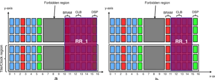
the implementation design step [14]. Such an automatic resizing employed by Vivado works as follows. The x-axis coordinates of the left and right vertical boundaries of each RR are first compared against the x-axis coordinates of the interconnect tiles on the fabric. If the left vertical boundary of a RR causes a violation, i.e., if the x-axis coordinate of the vertical boundary of the RR is equal to one of the x-axis coordinate of the interconnect tiles, then the location of the violating vertical boundary is updated by moving it one unit to the right on the x-axis. Conversely, if the right vertical boundary of a RR causes a violation, then the location of the violating vertical boundary is updated by moving it one unit to the left on the x-axis. This automatic resizing of RRs causes the shrinking of the RRs, as it is achieved by removing columns of resources from the original RR. As an example, consider Figure 4(a), which depicts an RR placement generated by DART at the partitioning/floorplanning stage, and Figure 4(b), which depicts the RR after it was resized by Vivado at the implementation stage. As it can be seen from Figure 4(b), the number of both BRAMs and DSPs is reduced by 6 units. Unless such future reduction of RR resources is properly modeled by the partitioning/floorplanning, it can cause the violation of a resource constraint during the implementation stage, i.e., there might not be enough resources for the RMs hosted after the RRs are shrunk.
CLB BRAM DSP x-axis y-axis Forbidden region T ile/Clock region 1 2 3 4 5 6 7 8 910111213141516 0 RR_1 CLB BRAM DSP y-axis Forbidden region 1 2 3 4 5 6 7 8 910111213141516 0 RR_1 a b
Figure 4: Illustration of the automatic Vivado resizing. (a) A RR that causes a back-to-back violation, and (b) the same RR after being automatically resized in Vivado.
A straightforward way to overcome this problem can be generat-ing placements with higher resource margins, such that when the RRs are shrunk there will still be enough resources. This approach can be suitable for the most abundant resources on the FPGA, i.e., CLBs, but it is an inefficient approach for the most scarce resources, i.e., BRAMs and DSPs. In a different approach, DART mitigates this condition by defining the following structural constraints: (i) Placements must be generated with a higher margin of CLBs; (ii) The left vertical columns of a RR placement cannot fall immediately to the left of a BRAM or a DSP column on the fabric; and (iii) The right vertical column of a RR placement cannot fall immediately to the right of a BRAM or a DSP column on the fabric.
Under these conditions, even if Vivado shrinks the RRs, it can be asserted that the excluded resources will neither be BRAMs nor DSPs (guaranteed by the last two constraints). The excluded CLBs will also be accounted for by the extra CLBs that are contained in the RR (guaranteed by the first constraint).
Xdc-generation sub-stage: In this sub-stage, the Cartesian place-ments that are generated by the MILP implementation sub-stage are mapped into their equivalent Xilinx FPGA pblock descriptions.
The contents of a Xilinx FPGA pblock description includes the name of the pblock, the unique IDs of the resources contained inside the pblock, and a set of properties of the pblock (e.g., "SNAP-PING_MODE"). Note that decoupling the MILP optimization from the xdc-generation allows re-using the optimization for similar FPGA families by only changing the way the xdc file is generated.
3.3
Static part generation
After performing partitioning/floorplanning and the generation of placement constraints, DART generates the Verilog implementation of the static part of the design from a parametric template, where the parameters are set from a configuration input provided by the designer. If no configuration input is provided by the designer, then the static part will be generated from a default configuration.
Figure 5 depicts the default static design generated by DART for two RRs (NRR = 2). Such a default static design contains black-box instances of the RRs and some AXI interconnects for connecting the RRs to the DRAM memory controller and the processing sys-tem (PS). The default configuration also includes a specification for the RR interfaces, which is generated considering the typical FPGA-based hardware acceleration setting in which SW-tasks and their corresponding RMs communicate using a shared-memory communication paradigm. Under this communication scheme, the RR interfaces should allow the RMs to read/write the main memory as well as receive control commands from the CPU, and be capa-ble of sending notification signals (interrupt) to the CPU. To this end, DART creates a common interface definition for the RRs that includes (i) one or more AXI master interfaces that allow RRs to access the system memory through the DRAM controller (AXI_M in Figure 5), (ii) an AXI slave interface to export a set of (memory-mapped) control registers (AXI_S in Figure 5), and (iii) an interrupt signal (INT in Figure 5).
By default, as denoted in Figure 5, DART assigns each RR with a single AXI master interface (denoted as AXI_M in Figure 5) to allow the hardware accelerators to access the DRAM memory through the DDR controller in the processing system (PS). DART also as-signs a single AXI slave interface (denoted as AXI_S in Figure 5) for each RR, which is used to map the control and data registers of the accelerator into the system memory space, hence making them available from the PS. Finally, for each RR, a designated interrupt signal (denoted as INT in Figure 5) is used to notify the completion of the HW-task to the PS. The default static design also pairs each RR with a partial reconfiguration decoupler (PR decoupler) mod-ule [19] to prevent temporary glitches during reconfiguration [20]. Alternatively, DART also allows the designer to override the default interface definition and specify a custom interface definition for the RRs.
All the RMs allocated to the same RR must have a matching name and interface with respect to the corresponding black-box RR in the static design. To match this requirement, DART creates a wrapper module that has the same name of the black-box RRs in the static design and wraps the RMs or IPs allocated to that black-box, hence guaranteeing name matching. After generating the static part and wrapping the RMs, DART synthesizes both the static part and the newly wrapped RMs, once again by using a similar approach described in Section 3.1. Finally, it stores the synthesized checkpoints in their appropriate locations in the project directory.
The outputs of this design stage, i.e., the set of synthesized RMs and the synthesized static part, are used in the routing and bitstream generation stage of the design.
As noted before, the designer can totally bypass the whole static generation stage when either intending to use a static design that contains hardware modules that cannot be disclosed (and hence can-not be generated by DART), or when requiring a fairly complicated static design with custom hardware modules and non-standard interconnections. In such a case, the designer can provide the syn-thesized checkpoints of the static part as an input to DART.
HW-task HW-task AXI M AXI S INT AXI S AXI interconnect AXI M AXI S INT AXI S AXI interconnect Concat DRAM Controller APU (ARM cores) AXI PS interconnects Decoupler Decoupler PL to PS ports PS to PL ports PL reconfigurable region PS PL static region
Figure 5: Illustration of a reconfigurable design containing the static part and two reconfigurable regions.
3.4
Routing and bitstream generation
The last stage in DART is the implementation stage, where by in-teracting with Vivado, and by iteratively swapping RMs into their corresponding RRs inside the static design, DART performs place-ment, routing, and finally bitstream generation for the design. To perform this design step, DART uses an implementation Tcl script generated by the implementation script generator available within the stage. This script, in combination with a set of pre-prepared Tclscripts, automates the Vivado implementation and bitstream generation. The auto-generated implementation script contains the description of the project in terms of the type of FPGA, the list of the RMs to be implemented, and different Tcl headers for Vivado. The script also includes one implementation configuration for each implementation iteration. An implementation configuration con-tains a set of details that are required to properly instruct Vivado, which include the mapping of RMs to the RRs, the XDC placement constraints, and routing and placement settings needed by Vivado. Listing 1 provides a pseudo-code that describes the generation of the implementation configurations as well as the correspond-ing implementation flow. The algorithm starts by initializcorrespond-ing the required variables for the implementation stage, which include the number of RRs, the number of RMs in each RR, and the partitioning allocation matrix as provided by the partitioning and floorplanning stage (line 3 - line 10). The number of implementation iterations and the number of implementation configurations are equivalent to the maximum number of modules allocated to partitions. After
the initialization, DART loads the synthesized static checkpoint into memory (line 14). Remember that the RRs inside the static checkpoint are black-boxes. Then, for each implementation iter-ation (line 16 - line 39), DART (i) creates a new implementiter-ation configuration (line 18), (ii) populates the configuration with ap-propriate RM-RR combinations (line 19 and line 28), and (iii) runs a Vivado place and route (line 30 - line 33) and stores the routed design checkpoints for a subsequent generation of the bitstream. At the end of each iteration, the implementation script swaps out the inserted modules and replaces them with their black-box equivalent for the next iteration (line 38). Finally, at the end of the implemen-tation iteration, DART generates the bitstreams using the stored routed checkpoints (line 42).
In case of an error in the Vivado implementation stage (place-ment, routing, or bitstream generation), DART performs a diagnos-tic step that starts by identifying the type of error, i.e., it extracts the error id by parsing the error reports generated by Vivado (line 47). If the error is among an enumerated list of supported errors, DART is able to fix it (line 48). Then, it performs the appropriate fix (line 49) and restarts the design step from the partitioning/floorplanning step (line 50 - line 51). If the error is not in the list, i.e., DART is not able to fix it, then it notifies the designer and aborts the design process (line 52). One example of an error that can be fixed by DART at the diagnostic step is related to the violation of a resource constraint, i.e., unavailability of resources in the RRs. This error can occur either due to an imprecise resource utilization estimation of Vivado at the synthesis stage, or from resource columns removed by the SNAPPING_MODE as discussed in Section 3.2. In case of such an error, DART fixes the error by increasing the resource margin discussed in Section 3.2.
4
EXPERIMENTAL EVALUATION
This section presents a case study application consisting of a hybrid accelerated system for image processing, which has been designed using DART. The system features a set of filter IPs for processing images and two binary neural networks (BNNs) for image classifi-cation. The considered application is, for instance, representative of those in driver-assistance systems, where a co-design approach is often used to accelerate computer vision, object detection, route planning, and actuation workloads.
Experimental Setup. The experimental evaluation has been per-formed using the PYNQ-Z1 board, which is equipped with the Zynq-7020 SoC from Xilinx (dual-core Cortex-A9 processor coupled with an Artix-7 family FPGA fabric). The FPGA fabric of the Zynq-7020 comprises 53200 LUTs, 140 BRAMs, 220 DSPs, and 106400 FFs. The SoC is connected to a shared DRAM memory of size 512MB.
DART has been implemented in C++, leveraging the Gurobi solver v.7.0.2 as a MILP optimization engine. The design flow has been tested on a 26-core Intel Xeon machine running Ubuntu Linux 18.04 and equipped with 132 GB of RAM. The placement, routing, and bitstream generation steps have been automated using Vivado 2018.3.
Image processing system The reconfigurable image processing system uses a set of filters and two BNNs from the BNN-FINN framework [15] for processing images stored inside the DRAM memory of the PYNQ-Z1 platform. Table 1 summarizes the activities
Listing 1: Pseudo-code of the implementation script.
1 run_implementation:
2 // These variables represent the partitioning result 3 num_part =NR R ; // number of partitions
4 num_mod[NR R ] = {...}// Number of RMs in each partition 5
6 // Number of implementation iterations 7 num_iter = max(num_mod); 8 9 // Partition allocations 10 partition[num_part][max_mod] = {{RM_1, RM_2, ...}, {RM_3, ...}}; 11 12 num_stored_check_points = 0;
13 // Load the synthesized static check point to memory 14 load_synthesized_static_design();
15
16 for(i = 1; i < num_iter; i++) {
17 // Create a new configuration 18 conf_ptr = create_config(i); 19 for(j = 0; k < num_part; j++) { 20 if(num_mod[j] > 0) { 21 num_mod[j]--; 22 RM = partition[j][num_mod[j]]; 23 set_config(conf_ptr, j, RM); 24 }else{ 25 RM = partition[j][0]; 26 set_config(conf_ptr, j, RM); 27 } 28 } 29 30 if(place_design(conf_ptr) != SUCCEEDED) 31 gotodiagnostics; 32 33 if(route_design(conf_ptr) != SUCCEEDED) 34 gotodiagnostics; 35 36 store_routed_checkpoint(); 37 num_stored_check_points++; 38 insert_black_box(); 39 } 40
41 for(i = 0; i < num_stored_check_points; i++) {
42 if(generate_bitstream() != SUCCEEDED))
43 gotodiagnositcs;
44 else returnOK;
45 46 diagnostics: 47 error_id = parse_error_report(); 48 if(error_list(error_id)) { 49 fix_error(error_id); 50 run_partitioning_floorplanning(); 51 gotorun_implementation
52 }else returnUNKNOWN_ERROR;
and parameters of the case study. The software part of the system consists of three periodic SW-tasks running on the Zynq ARM cores and periodically activated every 200 ms, 250 ms and 300 ms, respectively. The SW-tasks’ deadlines are equal to the periods, i.e., each SW-task must complete its execution before the next instance is released. The maximum times the SW-tasks can be suspended waiting for pending acceleration requests without missing their deadlines, which are referred to as slacks in the following, are 150 ms, 190 ms and 200 ms, respectively. The reconfigurable part of the system features three reconfigurable filter IPs (i) FAST corner detector (FASTx), (ii) Gaussian blur (Gaussian), and (iii) a finite input response filter (FIR), which were built using the OpenCV library included in Vivado HLS. The reconfigurable part also includes two BNNs, namely the LFCW1A1 network and a customized version of the CNVW1A1 network from the BNN-FINN framework [9]. Both neural networks use a 1-bit precision for weights and activations. The LFCW1A1 network features four fully-connected layers with 1024 neurons on each layer and it is trained to classify the MNIST dataset. The topology of the CNVW1A1 network used for this
Table 1: Parameters of the case study application.
SW-task id Period (ms) Slack (ms) RMs 1 200 150 FASTx, Gaussian, FIR
2 250 190 CNVW1A1
3 300 200 LFCW1A1
case study is inspired by the VGG-16 architecture and consists of four convolutional layers, two max-pooling layers, and two fully-connected layers. It is trained to classify the CIFAR-10 dataset. The combination of the two IP filters and two BNNs constitute the considered RMs. The three filters are used by the first SW-task, while the LFCW1A1 and CNVW1A1 networks are used by the second and third SW-tasks respectively.
All RMs use the same hardware interface, which includes one AXI4-lite slave interface, two AXI4 master interfaces, and an inter-rupt. The RMs are controlled by the SW-tasks using a set of control registers mapped through the AXI4-lite slave interface. Internally, when an RM is reconfigured on the FPGA and activated, it fetches data from the system DRAM and processes the image batch. The filter RMs are configured to process a batch of 24 images with a resolution of 176 x 144 pixels on each acceleration request, while the BNN RMs process a batch of 256 images on a single acceleration request. In the original implementation of the FINN accelerators, the parameters of the neurons, i.e., weights and activations, are loaded from DRAM memory into the hardware accelerators at run-time by the software. The software was also responsible for pre-processing a batch of images for classification. Hence, for both BNN accelerators, the total execution time for the inference of a batch was composed of (i) the time for pre-processing of a batch of input images, (ii) the time for loading of the neuron parameters from memory, and (iii) the time for the actual hardware inference. By profiling the accelerators, we have found that, despite its low memory footprint, the loading of the parameters of the accelerators from DRAM memory at run-time takes a large portion of the total execution time. To address this issue, the FINN accelerators of both networks have been modified to embed the neuron parameters directly into the accelerator during the generation of the bitstream. In this way, the loading of the parameters can be skipped and, once configured on the fabric, the BNN RMs are immediately ready to run. The design has been implemented with a PL clock frequency Fcl k of 125 MHz.
Before starting the DPR design flow, the WCETs of RMs are esti-mated using the following process: first, each RM is implemented individually on a static design, including only the RM under anal-ysis and the interconnects necessary to reach the PS ports. Then, the execution times are profiled using a bare-metal application. On each run, the profiling application (i) prepares the batch input images in a memory buffer, (ii) initiates a timer and starts the RM module, and (iii) when receiving the completion interrupt signal from the RM module, stops the timer. WCETs have been finally estimated by the maximum observed execution times. Due to the dataflow nature of the RM used in this experimental evaluation, limited fluctuations of the execution times occur.
For this experimental session, DART was configured to generate the default template for the static part, which with the exception
of one additional AXI master interface on each RR, is similar to the one reported in Figure 5. Hence, the static part includesNRR black-boxes for hosting the RRs,NRRdecouplers, and two AXI interconnects. One interconnect is used for connecting the AXI4 master interfaces exported by the RRs to the high-performance AXI interfaces of the PS. The other interconnect links one of the AXI general-purpose AXI master ports of the PS to the AXI4-lite slave interfaces exported by the RRs and the PR decouplers. The objective function to be minimized was the amount of wasted resources as formally defined in [12].
4.1
Performance analysis of DART
Table 2 reports the resource requirements of the RMs after the syn-thesis in the pre-processing stage. The results of the partitioning and the execution time of the inference are reported in Figure 6. Based on the input timing specifications and post-synthesis re-source consumption of the RMs, DART partitioned the HW-tasks into two RRs: the first RR, i.e., RR_1, hosts both BNNs, meanwhile, all the filter RMs are allocated to the second RR, i.e., RR_2. The reconfiguration time overheads of the RRs are 32 ms and 9 ms, respectively.
Table 2: Resource requirement of the RMs.
RM type Kernel size LUT FF BRAM DSP FASTx 5x5 2889 3474 6 8 Gaussian 5x5 2275 2055 8 3 FIR 5x5 4087 4122 4 9 CNVW1A1 - 13522 20112 85 0 LFCW1A1 - 19580 21443 103 0
It is worth noting that DART performs synthesis twice for each input RM, i.e., once at the pre-processing stage and the other one after the wrapping stage in the static part generation. Conversely, in the standard Xilinx DPR flow [20] (shown in Figure 2), the input modules are synthesized only once. These additional synthesis steps, in conjunction with the other extra design steps, can increase the running time of the design flow. To help contain the increase of the running time, the synthesis script generated by DART (in both the pre-processing step and the static part generation step) performs the synthesis in parallel for each RM, while in the standard Xilinx DPR flow the synthesis of the RMs is done sequentially.
CNVW1A1 LFCW1A1 FASTx Gaussian FIR
0 50 100 150 RR_2 RR_2 RR_2 RR_1 RR_1 110 70.9 27.2 19.01 38.44 RMs exe cution time (ms)
Figure 6: The partitioning and execution time of RMs. To measure the additional running time taken by DART to com-plete the design process, the image processing system was also
implemented by using the standard Xilinx DPR flow [20], under identical design conditions and on a similar design platform. The static part of the Xilinx flow, whose contents are identical to the static part generated by DART, is designed using the Vivado IP integrator. The RMs are also allocated in a similar way to how they are partitioned using DART and the floorplanning placements gen-erated by DART are also used inside the Xilinx flow. The results of the comparison are reported in Table 3. While it took 213 seconds to synthesize the five RMs using DART, the Xilinx DPR flow needed 642 seconds to synthesize the same number of RMs. The MILP im-plementation of the partitioning/floorplanning problem related to this case study produces the result in about 0.9 seconds. Note that, although the limited execution time of the MILP optimization can be attributed to the well formulation of the optimization problem, it can rise with the increase of the complexity of the design. The generation of the static part performed by DART is slower com-pared to the one performed by the standard design flow. This is due to the timing overheads in generating the static part and wrappers, in addition to the synthesis of the wrapped RMs in the same step. Finally, both approaches have a more or less similar bitstream gen-eration runtime. Overall, in terms of total design time, DART does slightly better (2.03% less in design run time) than the Xilinx flow. Nevertheless, it is worth remarking that the Xilinx flow tested in this experimental comparison is disadvantaged by the fact that the synthesis steps run sequentially, but also advantaged because (i) it had no manual floorplanning and partitioning overheads, since it was using the results provided by DART, and (ii) the time taken to design the static part is not taken into account.
Table 3: Comparison of the design run time of DART against the Xilinx DPR flow [20].
DART Time
(s)
Xilinx flow Time (s) Pre-processing 213 Partitioning floorplanning -Partitioning/floorplanning 0.9 RM Synthesis 642 Static part gen. 1409 static synthesis 1100 Impl. + bitstream. gen. 1901 implementation 1854
Total 3523 3596
5
RELATED WORK
During the last decade, several techniques have been proposed to provide support for non-expert designers via a full or partial au-tomation of the DPR design flow. However, most of the proposed works have one or more of the following shortcomings: (i) they focus on independently automating either the floorplanning or par-titioning design steps, hence they do not provide a globally-optimal solution for the integrated partitioning-floorplanning problem; (ii) they are based on older (deprecated) vendor design tools (e.g., most of the DPR automation tools proposed in literature only support ISE from Xilinx, which is the predecessor of Vivado); (iii) they do not support newer FPGA families and only provide outdated solutions. These approaches include tools that automate the individual design steps like partitioning [4, 17] and floorplanning step [7, 10, 12, 16].
Other tools that automate the full design flow are DAPR [21], GoA-head [1, 2], CoPR [18], and OpenPR [13]. These latter tools that fully automate the Xilinx DPR flow are reviewed in this section.
OpenPR and GoAhead are among the earliest DPR automation tools. OpenPR generates the static part of a DPR design from an input description of the system along with blocker macros to pre-vent the static region from using the routing resources inside the RRs. It supports the deprecated Xilinx PlanAhead tool for manually creating the floorplans of the design. GoAhead also allows designers to create a separate implementation flow for the static part and the RRs by utilizing blocker macros. The design flow in both of these tools requires an expertise in FPGA design and does not include a software-hardware co-design approach.
The partitioning in DAPR is based on an exhaustive search algo-rithm while CoPR uses a partitioning based on a graph clustering approach proposed in [17]. The floorplanner in DAPR uses a simu-lated annealing technique to generate placements while in CoPR the authors developed a custom floorplanning algorithm [16]. Both tools generate the bitstream by using Xilinx utilities and abstract the complexities of the DPR flow from the designer.
The DPR automation tool proposed in this work highly differs from CoPR and DAPR, as (i) it considers real-time requirements of SW-tasks and HW-tasks in a co-design approach, (ii) it inte-grates the partitioning and floorplanning in a DPR flow, into a single optimization problem and solves it using an optimization technique that guarantees the optimality of the solutions, (iii) it is based on existing vendor design tools and also considers newer FPGA families of architectures, and (iv) it provides the designer the option to generate the static region hence further minimizing the manual intervention. These significant differences prevented a fair comparison of CoPR and DAPR against DART.
Besides these tools, other researchers have also proposed alter-native models for the DPR tool flow. In [5], the authors proposed a framework to design DPR systems from a high-level unified mod-eling language (UML), while in [6] the authors create a custom modeling language to convert a Vivado HLS description of a system into a DPR implementation. Several researchers have also proposed design methodologies relying on bitstreams relocation [8, 11, 22]. Such approaches may offer some advantages in terms of flexibility. However, since the standard Xilinx flow does not support bitstream relocation, third-party tools may not offer the same level of depend-ability. Moreover, as bitstream relocation techniques are typically fabric-specific, they can limit the portability of the proposed flow.
6
CONCLUSION
This paper presented DART, a tool that fully automates the design flow of a real-time DPR-based system featuring both software and hardware components that run on FPGA-based SoC platforms un-der timing constraints. DART automates all the steps required by the DPR design flow, including partitioning, floorplanning, synthe-sis, placement, routing, and bitstream generation. DART has been experimentally evaluated with a case study consisting of a hybrid acceleration system featuring BNN accelerators and a set of filter IPs, which is executed upon a Xilinx PYNQ-Z1 platform.
Acknowledgment. This work has been supported by the EU H2020 project AMPERE under the grant agreement no. 871669.
REFERENCES
[1] Christian Beckhoff, Dirk Koch, and Jim Torresen. 2012. Go ahead: A partial reconfiguration framework. In 2012 IEEE 20th International Symposium on Field-Programmable Custom Computing Machines. IEEE, 37–44.
[2] Christian Beckhoff, Dirk Koch, and Jim Torreson. 2013. Automatic floorplanning and interface synthesis of island style reconfigurable systems with GOAHEAD. In International Conference on Architecture of Computing Systems. Springer, 303–316. [3] A. Biondi, A. Balsini, M. Pagani, E. Rossi, M. Marinoni, and G. Buttazzo. 2016. A
Framework for Supporting Real-Time Applications on Dynamic Reconfigurable FPGAs. In Proceedings of the IEEE Real-Time Systems Symposium (RTSS). [4] A. Biondi and G. Buttazzo. 2017. Timing-aware FPGA Partitioning for Real-Time
Applications Under Dynamic Partial Reconfiguration. In Proceedings of the 11th NASA/ESA Conference on Adaptive Hardware and Systems (AHS).
[5] David de la Fuente, Jesús Barba, Julián Caba, Pablo Peñil, Juan Carlos López, and Pablo Sánchez. 2016. Building a Dynamically Reconfigurable System Through a High-Level Development Flow. In Languages, Design Methods, and Tools for Electronic System Design. Springer, 51–73.
[6] Rohit Kumar and Ann Gordon-Ross. 2015. An automated high-level design framework for partially reconfigurable FPGAs. In 2015 IEEE International Parallel and Distributed Processing Symposium Workshop. IEEE, 170–175.
[7] Tuan D.A. Nguyen and Akash Kumar. 2016. PRFloor: An Automatic Floorplanner for Partially Reconfigurable FPGA Systems. In Proceedings of the 2016 ACM/SIGDA Int. Symposium on Field-Programmable Gate Arrays (FPGA ’16).
[8] Roel Oomen, Tuan Nguyen, Akash Kumar, and Henk Corporaal. 2015. An auto-mated technique to generate relocatable partial bitstreams for Xilinx FPGAs. In 2015 25th International Conference on Field Programmable Logic and Applications (FPL). IEEE, 1–4.
[9] BNN-PYNQ project. 2020. . https://github.com/Xilinx/BNN-PYNQ. (2020). [On-line; accessed 11-January-2020].
[10] M. Rabozzi, G. C. Durelli, A. Miele, J. Lillis, and M. D. Santambrogio. 2017. Floor-planning Automation for Partial-Reconfigurable FPGAs via Feasible Placements Generation. IEEE Transactions on Very Large Scale Integration (VLSI) Systems 25, 1 (Jan 2017), 151–164. https://doi.org/10.1109/TVLSI.2016.2562361
[11] Jens Rettkowski, Konstantin Friesen, and Diana Göhringer. 2016. RePaBit: Auto-mated generation of relocatable partial bitstreams for Xilinx Zynq FPGAs. In 2016 International Conference on ReConFigurable Computing and FPGAs (ReConFig). IEEE, 1–8.
[12] Biruk B. Seyoum, Alessandro Biondi, and Giorgio C. Buttazzo. 2019. FLORA: FLoorplan Optimizer for Reconfigurable Areas in FPGAs. ACM Trans. Embed. Comput. Syst. 18, 5s, Article Article 73 (Oct. 2019), 20 pages. https://doi.org/10. 1145/3358202
[13] Ali Asgar Sohanghpurwala, Peter Athanas, Tannous Frangieh, and Aaron Wood. 2011. OpenPR: An open-source partial-reconfiguration toolkit for Xilinx FP-GAs. In 2011 IEEE International Symposium on Parallel and Distributed Processing Workshops and Phd Forum. IEEE, 228–235.
[14] ug909-vivado-partial-reconfiguration user guide. 2018. . https: //www.xilinx.com/support/documentation/sw_manuals/xilinx2018_1/ ug909-vivado-partial-reconfiguration.pdf. (2018). [Online; accessed 27-May-2020].
[15] Yaman Umuroglu, Nicholas J. Fraser, Giulio Gambardella, Michaela Blott, Philip Leong, Magnus Jahre, and Kees Vissers. 2017. FINN: A Framework for Fast, Scal-able Binarized Neural Network Inference. In Proceedings of the 2017 ACM/SIGDA International Symposium on Field-Programmable Gate Arrays (FPGA ’17). ACM, 65–74.
[16] Kizheppatt Vipin and Suhaib A. Fahmy. 2012. Architecture-Aware Reconfiguration-centric Floorplanning for Partial Reconfiguration. In Proceed-ings of the 8th Int. Conf. on Reconfigurable Computing: Architectures, Tools and Applications (ARC’12).
[17] Kizheppatt Vipin and Suhaib A Fahmy. 2013. Automated partitioning for partial reconfiguration design of adaptive systems. In 2013 IEEE International Symposium on Parallel & Distributed Processing, Workshops and Phd Forum. IEEE, 172–181. [18] Kizheppatt Vipin and Suhaib A Fahmy. 2015. Mapping adaptive hardware systems
with partial reconfiguration using CoPR for Zynq. In 2015 NASA/ESA Conference on Adaptive Hardware and Systems (AHS). IEEE, 1–8.
[19] Xilinx [n. d.]. Partial Reconfiguration Decoupler, LogiCORE IP Product Guide. Xilinx.
[20] Xilinx [n. d.]. Vivado Design Suite User Guide: Partial Reconfiguration. Xilinx. [21] Shaon Yousuf and Ann Gordon-Ross. 2016. An automated hardware/software
co-design flow for partially reconfigurable FPGAs. In 2016 IEEE Computer Society Annual Symposium on VLSI (ISVLSI). IEEE, 30–35.
[22] Rafael Zamacola, Alberto García Martínez, Javier Mora, Andrés Otero, and Ed-uardo de La Torre. 2018. IMPRESS: Automated Tool for the Implementation of Highly Flexible Partial Reconfigurable Systems with Xilinx Vivado. In 2018 International Conference on ReConFigurable Computing and FPGAs (ReConFig). IEEE, 1–8.


![Table 3: Comparison of the design run time of DART against the Xilinx DPR flow [20].](https://thumb-eu.123doks.com/thumbv2/123dokorg/8286290.131132/9.918.98.430.854.979/table-comparison-design-time-dart-xilinx-dpr-flow.webp)
