Dilute Magnetic Semiconductors: the role of 𝑀𝑛
in 𝐺𝑎𝑀𝑛𝐴𝑠(001) and 𝑀𝑛/𝐺𝑎𝐴𝑠(001) surfaces
A thesis presented by
Stephen Denny Thorpe
to
Physics Department
in partial fulfillment of the requirements
for the degree of
Doctor of Philosophy
in the subject of
Physics
University of Rome "Tor Vergata"
Rome, Italy - December 2009
Supervisors PhD Coordinator
Prof. A. Balzarotti Prof. P. Picozza Dr. S.
Colonna (ISM-CNR)
© [2009] by [Stephen Denny Thorpe]
Index
1. Introduction
3
1.1 Spintronics
3
1.2 Magnetic semiconductor
5
References
7
2. Non magnetic semiconductor 𝑮𝒂𝑨𝒔 surface
9
2.1 General aspects
9
2.2 The electronic counting rule
11
2.3 Arsenic rich structure: (2 × 4) and (4 × 4) reconstructions
14
2.4 (110) surface structure
23
References
27
3. Dilute Magnetic Semiconductor (DMS)
31
3.1 Overview
31
3.2 Structural properties
32
3.3 Electronic properties
34
3.4 Magnetic properties
36
3.5 Defects
39
3.6 𝑀𝑛 deposition on 𝐺𝑎𝐴𝑠
41
References
43
4. Experimental Techniques
47
4.1 Overview
47
4.2 Molecular Beam Epitaxy (MBE)
47
4.2.1. Growth of 𝐺𝑎𝐴𝑠 and 𝐺𝑎𝑀𝑛𝐴𝑠 with MBE
49
4.2.2. MBE growth
52
4.2.3. Molecular flux and growth rate measured by RHEED
54
4.3 Low Energy Electron Diffraction (LEED) and Reflected High Energy
Electron Diffraction (RHEED)
oooooooooooooooooooooooooo
57
4.3.1. Theory of surface scattering
57
4.3.2. LEED
61
4.4 Electron Energy Loss Spectroscopy
i
67
4.4.1. Small angle inelastic scattering
71
4.5 Scanning Tunneling Microscopy (STM)
I
75
4.6
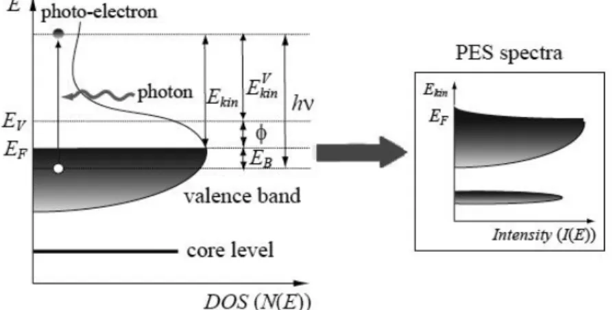
Photoemission Spectroscopy (PES) and Photoelectron Diffraction
(PED)
79
4.6.1. Photoelectron Diffraction (PED)
81
4.7
Reflectivity Anisotropy Spectroscopy (RAS)
85
References
88
5. Growth and characterization of 𝑮𝒂𝑨𝒔 and 𝑮𝒂
𝟏−𝒙𝑴𝒏
𝒙𝑨𝒔
91
5.1 Introduction
0
91
5.2 𝐺𝑎𝐴𝑠 preparation
0
92
5.3 𝐺𝑎𝑀𝑛𝐴𝑠 preparation
0
96
5.4 Magnetic characterization
0
97
5.5 Structural characterization
101
References
107
6. 𝑮𝒂𝑴𝒏𝑨𝒔(𝟎𝟎𝟏) and 𝑴𝒏/𝑮𝒂𝑨𝒔(𝟎𝟎𝟏) surface
characterization
111
6.1 Introduction
111
6.2
𝐺𝑎𝑀𝑛𝐴𝑠(001)
112
6.2.1. Experimental results
115
6.3
𝑀𝑛/𝐺𝑎𝐴𝑠(001). Experimental results
126
References
142
7. Conclusions
145
Appendix. Future development
147
A. Cross sectional STM measurement of 𝑮𝒂𝑴𝒏𝑨𝒔(𝟎𝟎𝟏) surface 147
B. STM measurement on 𝑴𝒏: 𝑮𝒂𝑨𝒔 𝟎𝟎𝟏 𝜷𝟐(𝟐 × 𝟒) surface 152
Chapter 1
Introduction
1.1. Spintronics
Spintronics is an emergent technology that exploits the quantum feature of the electron to spin and makes use of its charge state [1,2]. The spin itself is manifested as a detectable weak magnetic energy state characterized as spin up or spin down. Conventional electronic devices rely on the transport of electrical charge carriers – electrons – to a semiconductor such silicon or gallium arsenide. Now, however, device engineers and physicists are inevitably dealing with the looming presence of quantum mechanics and are trying to exploit the spin of the electron rather than its charge. Devices that rely on the electron spin to perform their function form the foundations of spintronics (short of spin-based electronics), also known as magnetoelectronics [3]. Spintronics devices are smaller than 100 𝑛𝑚 in size, more versatile and faster than those commercially used for making up processing chips and circuit elements. The potential market is worth hundreds of billions of Euros per annum [4].
Spintronics burst on the scene in 1988 when Albert Fert and Peter Grünberg discovered a very powerful effect called Giant Magnetoresistance (GMR) that rewarded their efforts with the Nobel prize in 2007: “The discovery of GMR opened the door to a new field of science, magnetoelectronics (or spintronics), where two fundamental properties of the electron, namely its charge and its spin, are simultaneously manipulated. While emerging nanotechnology was an original prerequisite for the discovery of GMR, at present magnetoelectronics are in turn a driving force for new applications of nanotechnology. In this field, demanding and exciting scientific and technological challenges become
intertwined, strongly reinforcing progress.”1 The GMR results from subtle electron- spin effects in ultra thin multilayers of magnetic materials which cause huge changes in their electrical resistance when a magnetic field is applied. This mechanism resulted in the first spintronics device in the form of the spin valve. The incorporation of GMR materials into read heads allowed the storage capacity of a hard disk to increase from one to 20 gigabits. In 1997, IBM launched GMR read heads, into a market worth around a billion dollars per annum. This field of research is relatively young and it is difficult to forecast how it will evolve. This aspect is directly depending on new materials that the scientific community of Material Science is studying such as magnetic semiconductor and an exotic and more extreme effect called Colossal Magnetoresistance (CMR) [5].
Spintronics materials research is an important area of the nanomaterials science to both fundamental scientific research and industrial applications. These new devices are expected to be non-volatile, versatile, fast and capable of simultaneous data storage and processing, while consuming less energy. They are playing an increasingly significant role in high-density data storage, microelectronics, sensors, quantum computing, bio-medical applications, etc. It is expected that the development of spintronics to the microelectronics industry might be comparable to the development that the transistor roused 50 years ago. Nowadays every computer user already has a spintronics device on his desktop, as all modern computers use the spin valve to read and write data on their hard drive. It was immediately followed by the discovery of Tunneling Magnetoresistance (TMR) leading to the magnetic tunnel junction that has been utilized for the Magnetic Access Memory (MRAM) in commerce since 2004 [6, 7]. At present the research is concentrated on the fabrication of spin transistors and spin logics devices integrating magnetic and semiconductors, with the aim of improving the existing capabilities of electronic transistors and logics devices so that the future computation and thus the future computers could become faster and consume less energy.
The four main investigation areas in spintronics are:
I. Understanding the fundamental physics, such as spin-dependent transports across the magnetic/semiconductor interfaces and spin coherence length in semiconductors;
1
II. Synthesizing suitable spintronics materials with as higher as possible Curie Temperature, large spin polarization at the Fermi level and matching conductivity between the magnetic and semiconductor materials;
III. Fabricating devices with nanometers feature sizes and developing new techniques for mass production;
IV. Integrating spin-devices with current microelectronics and computing and elaborating again all the logics based on the quantum mechanics in order to improve the development of the quantum computing.
1.2. Magnetic semiconductors
The first discovery of interplay between semiconducting bulk properties and ferromagnetism was the europium chalcogenides, a semiconductors spinels produce a great interest and the desire to improve the study of this materials in the 1960’𝑠 and 1970’𝑠. In the 80’𝑠 the technical difficulties of the preparation of single crystals and the low Curie temperature made this interest to become much lower. The second generation of ferromagnetic semiconductor was based on non magnetic semiconductors alloyed with magnetic elements (mostly transition metals). Such alloys between a nonmagnetic semiconductor host and magnetic elements in a low concentration (about 2%) are called dilute magnetic semiconductors (DMS) [8]. The first choice was 𝐼𝐼 − 𝑉𝐼 compounds (like 𝑍𝑛𝑆𝑒 and 𝐶𝑑𝑇𝑒) because of the compatibility of the valence of cations (𝑠2) with that of typical magnetic elements 3𝑑54𝑠2 like 𝑀𝑛. These materials exhibit a great change in their properties upon application of magnetic fields due to the exchange interaction between the conduction carriers and the localized magnetic moments. This magnetism was limited to paramagnetism or spin glasses resulting from antiferromagnetic superexchange interactions among magnetic ions. The discovery of ferromagnetism in 𝐼𝐼𝐼 − 𝑉 based DMS’s (𝐼𝑛, 𝑀𝑛)𝐴𝑠 and (𝐺𝑎, 𝑀𝑛)𝐴𝑠 [9], has opened a unique opportunity of introducing ferromagnetism in the semiconductor which was already in use in electronics applications (lasers and transistors) and integrating ferromagnetism in semiconductor heterostructures. The highest transition temperature (𝑇𝑐) obtained in (𝐺𝑎, 𝑀𝑛)𝐴𝑠 is 170𝐾 [10], still below room temperature but
above liquid nitrogen temperature so to be useable for special applications. However, a model for the ferromagnetism capable to describe a number of experimental observation suggests a route to above room temperature ferromagnetism in the family of tetrahedrally bonded semiconductors like 𝐼𝐼𝐼 − 𝑉 compounds.
The aim of this thesis is to study the behavior of 𝑀𝑛 in the 𝐺𝑎𝑀𝑛𝐴𝑠(001) surface and to increase the comprehension of 𝑀𝑛 incorporation on 𝐺𝑎𝐴𝑠 lattice by depositing 𝑀𝑛 on the 𝐺𝑎𝐴𝑠(001) surface with successive annealing treatments. The target is to understand the procedure for grow high quality 𝐺𝑎𝑀𝑛𝐴𝑠 films with high 𝑇𝑐 (ideally room temperature) useful for several applications in spintronics and, furthermore, to improve knowledge of electronic properties for spin injection [11]. In Chapters 2 and 3 the 𝐺𝑎𝐴𝑠 and 𝐺𝑎𝑀𝑛𝐴𝑠 structures will be explained with all the surface reconstructions and electronic and magnetic properties. In Chapter 4 an overview of all experimental techniques used in this thesis will be shown. Chapter 5 is dedicated to the growth of 𝐺𝑎𝐴𝑠 and 𝐺𝑎𝑀𝑛𝐴𝑠 with magnetic and structural characterizations. All the experimental results are presented and discussed in Chapter 6.
References
[1] S. A. Wolf, D. D. Awschalom, R. A. Buhrman, J. M. Daughton, S. von Molnár, M. L.
Roukes, A. Y. Chtchelkanova, and D. M. Treger Science 294 1488 (2001).
[2] Masaaki Tanaka Journal of Crystal Growth 278 25-37 (2005). [3] Gary A. Prinz Science 282 1660 (1998).
[4] David D. Awschalom and Michael E. Flattè Nature Physics 3 153 (2007). [5] A. P. Ramirez J. Phys. Condens. Matter 9 8171–8199 (1997).
[6] T. Dietl and H. Ohno Materials Today 9 18 (2006).
[7] Katrin Pappert, Silvia Hümpfner, Charles Gould, Jan Wenisch, Karl Brunner, Georg
Schmidt, Laurens W. Molenkamp Nature Physics 3 573 (2007).
[8] H. Munekata, H. Ohno, S. von Molnar, Armin Segmüller, L. L. Chang, and L. Esaki
Physical Review Letters 63 1849 (1989).
[9] H. Ohno Science 281 951 (1998).
[10] Kenichi Ohno, Shinobu Ohya and Masaaki Tanaka Journal of Superconductivity and
Novel Magnetism 20 417 (2007).
[11] Y. Ohno, D. K. Young, B. Beschoten, F. Matsukura, H. Ohno and D. D. Awschalom
Chapter 2
Non magnetic semiconductor 𝑮𝒂𝑨𝒔
surface
2.1. General aspects
The clean 𝐺𝑎𝐴𝑠 is a typical 𝐼𝐼𝐼 − 𝑉 semiconductor compound with a zincblende structure where 𝐺𝑎 occupy the cubic cell and 𝐴𝑠 tetrahedrical position. The natural growth surface is a face of the cubic cell, typically the 001 surface. Because the zincblende crystal structure has a tetrahedral coordination in the bulk, the polar 𝐺𝑎𝐴𝑠(001) surface could be 𝐺𝑎 or 𝐴𝑠 terminated (fig. 2.1). Compared to 𝐺𝑒 and 𝑆𝑖 and to the 𝐺𝑎𝐴𝑠 cleaved (110) surface, a successful sample preparation is more difficult for 𝐺𝑎𝐴𝑠(001) [1,2]. In fact preparation of a well ordered and clean 𝐼𝐼𝐼 − 𝑉 (001) surface usually requires a growth apparatus such as molecular beam epitaxy (MBE) or metal organic chemical vapor deposition (MOCVD) reactor. After the growth an 𝐴𝑠 capping layer deposited on the sample surface can be used to prevent air contamination. The 𝐴𝑠 decapping technique can be used to produce high quality surfaces, but one must be careful and the expected results are often missing in quality in comparison to MBE samples.
Fig.2.1. 𝐺𝑎𝐴𝑠 bulk terminated structure. Green balls are 𝐴𝑠 atoms, red balls are 𝐺𝑎 atoms.
An alternative method of preparation is to treat the 𝐺𝑎𝐴𝑠(001) surface with HCl and propanol in 𝑁2 flux, followed by annealing in UHV. Anyway, in both cases annealing without 𝐴𝑠 flux can lead to the formation of 𝐺𝑎 droplets and to non stoichiometric surfaces since 𝐴𝑠 is volatile. Moreover, 𝐺𝑎𝐴𝑠(001) surfaces involve an additional degree of freedom due to stoichiometry dependent reconstructions. Depending on the thickness of the grown sample and on experimental conditions, the surface exhibits a number of reconstructions, starting with the most 𝐴𝑠 rich phase, which has the 𝑐(4 × 4) symmetry, through the (2 × 4) phase including the off-phase 𝑐(2 × 8) (similar to (2 × 4) phase but with 2× periodicity respect to previous row), (1 × 6), (4 × 6), and ending with the 𝐺𝑎 stabilized phases 4 × 2 and 8 × 2 . Experimental and theoretical studies have resulted in the establishment of two basic and general features in the structure of the 𝐺𝑎𝐴𝑠(001) surface. To find the reconstruction with lowest energy for a given anion chemical potential 𝜇𝐴 that depends on the preparation conditions (like temperature and pressure), the surface stoichiometry and geometry at a given 𝜇𝐴, has to be compared with the surface energy 𝛺𝑆 determined by surface models (in fig. 2.2 the example of 𝐺𝑎𝐴𝑠(001) is presented). At a certain temperature there is a probability 𝑐𝑠 that one surface phase is formed [3]:
𝑐𝑠 ≈ 𝑒𝑥𝑝 − 𝑚 × 𝑛 𝛺𝑠 𝐾𝐵𝑇
where 𝑚 × 𝑛 𝛺𝑠 is the formation energy of one determined surface 𝑚 × 𝑛 reconstruction. In general this probability is also influenced by entropy effect (𝑑𝛺𝑠 = −𝑆𝑠𝑢𝑟𝑓𝑎𝑐𝑒 𝑑𝑇) which can modify the stability of a phase at a given temperature. In the gaseous phases the effect of temperature 𝑇 and pressure 𝑝 upon the chemical potentials is much more important than for condensed states. The chemical potentials 𝜇𝑖 depend logarithmically upon 𝑇 and 𝑝 and the large variation of 𝜇𝑖 can be used to control the state of condensed phases in equilibrium with the gas.
The stability of all reconstructions can be substantiated by a simple but practical rule, the electron counting rule (ECR) [4,5], illustrated in the next paragraph.
Fig. 2.2. 𝐺𝑎𝐴𝑠(001) surface energies as a function of 𝐺𝑎 chemical potential for a unit cell.
2.2. The electron counting rule (ECR)
The atoms in the 𝐺𝑎𝐴𝑠 bulk are 𝑠𝑝3 hybridized. Two hybridized orbitals, one from each type of atom, combine to form a two orbitals: bonding and antibonding. But at the surface some hybrid orbitals cannot form bonds, so partially filled 𝑠𝑝3 dangling bonds will remain without reconstruction. Final dangling bonds energies can be estimated from the starting energies of the 𝑠 and 𝑝 atomic levels. In fig. 2.3 can be seen the dangling bond energy level for 𝐺𝑎 (electropositive element) that should be empty since it is in the conduction band, and the dangling bond energy level for 𝐴𝑠 (electronegative element) that should therefore be filled since it is in the valence band. To achieve this, electrons transfer from 𝐺𝑎 dangling bond to 𝐴𝑠 dangling bond. However, charge transfer induces additional static electric capacitance energy due to charge accumulation, the resulting surface becomes energetically unstable unless some amount of dimers is removed from the surface to compensate this energy and achieve charge neutrality. Dimer missing characterizes the reconstruction of the 𝐺𝑎𝐴𝑠 001 surface, which is further generalized by ECR.
Fig.2.3. The energy levels diagram of 𝐺𝑎𝐴𝑠 and its application to the 001 𝐴𝑠 –terminated surface. The hybrid energy levels 𝐸, are derived from the 𝑠 and 𝑝 orbitals; two of the 𝐴𝑠 hybrids
are unbounded 𝑠𝑝3 hybrid dangling bonds. Subsequent dimerization produces an 𝐴𝑠 − 𝐴𝑠 dimer bonding and antibonding combination, leaving one 𝐴𝑠 dangling bond per atom at the hybrid energy, 𝐸 Charge transfer from the underlying 𝐺𝑎 into this state produces a filled lone pair orbital.
ECR requires that a stable surface structure is formed when the number of available
electrons in the surface layer exactly fills all dangling bond states in the valence band, leaving those in the conduction band completely empty. This rule dictates that there should be no net charge leaving on the surface. With further lattice distortion, the surface energy band structure becomes more semiconducting, whereas partially filled dangling bonds may lead to a metallic surface resulting in a unstable structure. In general surface reconstructions and surface relaxations follow 3 guiding principles:
1. A surface tends to minimize the number of dangling bond by the formation of new bonds. The remaining dangling bonds tend to be saturated;
2. A surface tends to compensate charges;
3. A semiconductor surface tends to be insulating or semiconducting.
The lowest energy structure is obtained with filled states dangling bonds on the electronegative element (with 𝑉𝑛 valence electrons) and empty dangling bonds on the electropositive element (with 𝑉𝑝 valence electrons). To apply the principles exposed above
to 𝐺𝑎𝐴𝑠 001 , we consider the 𝐴𝑠 −rich surface with a missing 𝐴𝑠 −dimer; the unit cell consists of 𝐷 dimers with every 𝑁 −th dimer missing, namely the surface has the 2 × reconstruction; so the surface forms a 2 × 𝑁 reconstruction with 2 × being the periodicity coming from the formation of 𝐴𝑠 dimers and 𝑁 × being the periodicity of missing surface dimers, leaving 𝐷 dimers per unit cell where 𝐷 ≤ 𝑁. We now count up the numbers of electrons required to satisfy these conditions and equate that with the numbers of electron available in order to determine the relationship between 𝑁 and 𝐷. Thus from Fig. 2.4 each top layer dimer requires six electrons (two in each dangling bonds and two in the dimer bond), making 6𝐷 electrons in total in the top layer per surface crystallographic cell.
Fig.2.4. The bonds and dandling bonds, both filled (shaded) and empty (open), for 2 × 𝑁 a unit cell on the surface of a polar semiconductor with the zincblende crystal structure, where the 2 periodicity arises from missing dimers.
A total of 8𝐷 electrons are required to bond the dimers to the second layer of atom. The numbers of electrons available from the top-layer atoms is 2𝑉𝑛𝐷, and the numbers of electrons available from the second layer is 2𝑉𝑝𝑁 2 (since half of the total electrons from the second layer are involved in bonding to the third layer). Thus, a stable structure is obtained when: 6𝐷 + 8𝐷 = 2𝑉𝑛𝐷 + 2𝑉𝑝𝑁 2 . In the case of our system, 𝑉𝑛 = 5 and 𝑉𝑝 = 3, thus 4𝐷 = 3𝑁. The smallest unit cell that satisfies this condition is the unit cell containing three dimers with every fourth dimer missing. If deeper layer atoms are involved in the reconstruction, consideration of ECR will give rise to additional two dimers models.
2.3. Arsenic rich surface structure: 2 × 4 and 4 × 4 recostruction
The 𝐺𝑎𝐴𝑠(001) surface shows a 𝑐(4 × 4) symmetry for 𝐴𝑠 −rich conditions, but changes its periodicity to (2 × 4)/𝑐(2 × 8) and finally (4 × 2)/𝑐(8 × 2) as the surface gets more 𝐺𝑎 −rich. In addition, a large variety of transient structures or apparent symmetries such as (2 × 3), (2 × 1), (3 × 1), (3 × 6), (2 × 6), (6 × 6), (4 × 6), etc., are reported [1– 4]. The large number of observed surface structures have prompted the necessity to classify and understand them from a more general point of view. For example the ECR was recognized to govern many reconstructions. The ECR together with the dimerization as the major mechanism to reduce the number of dangling bonds on 𝐺𝑎𝐴𝑠(001) surface were able to successfully explain a large number of surface geometries. This success prompted Mönch to write *6+: “The electronic energy of such surfaces will be lowest when
a) surface atoms in the top layer are forming dimers and
b) dangling bonds are filled on surface anions (𝐴𝑠) and are empty at the surface cations
(𝐺𝑎)”.
The (2 × 4) reconstruction has been extensively studied because is usually observed during MBE growth in 𝐴𝑠 −rich condition. Several (2 × 4) structural models, summarized in fig. 2.5, satisfying 𝐸𝐶𝑅 have been proposed.
Fig.2.5. Top and side views of the relaxed 𝐺𝑎𝐴𝑠 001 2 × 4 𝛼, 𝛽2, and 𝛽 phases. Large (small) filled circles indicate top-(third-) layer 𝐴𝑠 atoms, whereas large (small) empty circles represent second- (fourth-) layer 𝐺𝑎 atoms. The 𝛾 phase has five layers [26].
The (2 × 4) 𝐺𝑎𝐴𝑠(001) surface is known to exhibit a very rich variety of ordered phases whose occurrence depends on the preparation conditions [7,8] and correlating, characteristic patterns with the surface stoichiometry, can be distinguished between three (2 × 4) phases, called 𝛼, 𝛽 and 𝛾 [9]. The 𝛼 phase occurs at the highest substrate temperature and was suggested to correspond to a geometry combining two 𝐴𝑠 dimers in the uppermost atomic layer with 𝐺𝑎 − 𝐺𝑎 bonds in the layer underneath. Schmidt et al. showed recently that the same stoichiometry can be realized with an energetically more favored structure, called 𝛼2(2 × 4) [10]. This structure, shown in fig. 2.5, is 0.034 𝑒𝑉 per (1 × 1) unit cell lower in energy than the 𝛼 model. The 𝛼 structure will be unstable with respect to 𝛼2 irrespective of the surface-preparation conditions. The structural difference consists in the fact that the 𝛼 model has two 𝐴𝑠 − 𝐴𝑠 dimers in the first layer and the 𝛼2 has one 𝐴𝑠 − 𝐴𝑠 dimer in the first layer and one in the third layer (Fig. 2.5 (c) and Fig. 2.5 (e)). The 𝛽 phase (Fig. 2.5 (a), which is stable for more anion-rich conditions, was explained originally by the three-dimer model due to Chadi [11]. Northrup and Froyen [12] later showed that a somewhat modified structure, called 𝛽2 (Fig. 2.5 (b)), leads to a lower electrostatic energy and is energetically favored. The structure model shown in Fig. 2.5(a) contains three 𝐴𝑠– 𝐴𝑠 dimers, and is now referred to as the 𝛽(2 × 4) model. The model shown in Fig. 2.5(b) contains two 𝐴𝑠 dimers in the outermost atomic layer with a third 𝐴𝑠 dimer situated in the third atomic layer, within the trench formed due to missing dimers (so called 𝛽2(2 × 4) model). The STM images in Fig. 2.6 shows the 𝛽2 structure with the two dimers in the top layer inside the unit cell. The reconstruction depends on the growth conditions [12].
Fig. 2.6. STM image of 𝛽2(2 × 4) at -2.1 V and 0.3 nA. The white rectangle represents the unit cell [12].
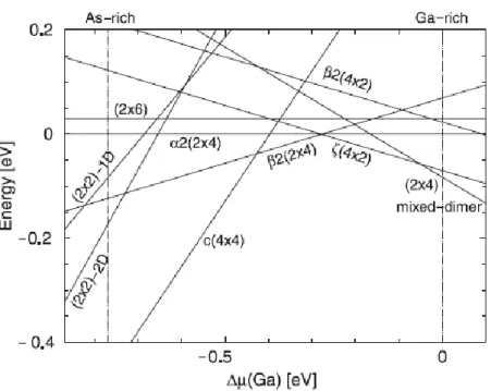
While the ECR gives an indication of which structures might be stable and which should not be, it does not allow us to discriminate energetically between two structures complying with the electron-counting principle. A major progress in that respect was the work by Northrup and Froyen on the role of electrostatic interactions between the surface structural units [12]. They showed that Coulomb repulsion between negatively charged 𝐴𝑠 dimers favours the two-dimer 𝛽2(2 × 4) structure over the three-dimer 𝛽(2 × 4) structure. Based on similar electrostatic arguments, Schmidt et al. [10] predicted recently that a one-dimer 𝛼2(2 × 4) structure should be lower in energy than the hitherto accepted 𝛼(2 × 4) model. The estimation of relative surface energies from empirical concepts was further refined by Zhang and Zunger [14], who observed that the large collection of equilibrium surface structures is built from a limited number of recurring local structural motifs, such as threefold-coordinated pyramidal anions or surface dimers. The energies of these structural motifs can be obtained from a fit to the results of ab initio calculations on flat surfaces and bulk defects. Based on motif energies obtained in such a way, Zhang and Zunger estimated the surface energies for reconstructions larger than what could be dealt with from first principles at that time. Starting from atomic energy levels and bonding energies, Mirbt et al. derived a very simple expression called a surface reconstruction parameter in order to assess the stability of reconstruction models. According to this parameter, for the stability of
𝐼𝐼𝐼 − 𝑉 surfaces it is required that under cation-rich conditions the sum of anion dangling bonds and anion–anion bonds should be minimized. For anion-rich conditions the expression 𝑁𝑎 − 𝑁𝑎−𝑎+ 2𝑁𝑐−𝑐 needs to be minimized, where 𝑁𝑎 is the number of anion dangling bonds and 𝑁𝑎−𝑎 and 𝑁𝑐−𝑐 denote the numbers of anion–anion and cation–cation bonds. Later, the same group pointed out how local stress may modify these rules [15].
The 𝛽 and 𝛽2 models were found to have the same energies and to be more stable than the structure with only two dimers (Fig. 2.5(c)). Other total-energy calculations [16, 17, 18] confirmed this result. The actual occurrence of the 𝛽2(2 × 4) structure was proven by in situ grazing incidence 𝑋 − 𝑟𝑎𝑦 diffraction measurements [19], dynamical RHEED analysis [20] and very recently by highly resolved STM images [21]. The 𝛾 phase, finally, occurring for even more 𝐴𝑠-rich surfaces, was found to be a mixture of the 𝛽 phase and the 𝑐(4 × 4) phase, with the surface 𝐴𝑠 coverage varying depending on the actual growth conditions [22, 23]. Moll et al. [18] performed total-energy calculations for several 𝑐(4 × 4) structures. In agreement with the present study, Sauvage-Simkin et al. [24] find the three dimers structure to have the lowest energy (cf. Fig. 2.5). Avery et al. proposed that the 𝛾 phase involves kink formation due to the preferential occupation by additional 𝐴𝑠 atoms of second layer 𝐺𝑎 sites in the missing dimer trenches of the 𝛽2(2 × 4) structure [25]. The 𝛼 and 𝛽 phases emerge under less and more 𝐴𝑠-rich MBE conditions, respectively. The 𝐺𝑎𝐴𝑠(001)(2 × 4) surface consists of the well-ordered 𝛽2 domains obtained in a relatively wide range of substrate temperature (500 − 600 °𝐶) under 𝐴𝑠 fluxes (about 3 ∙ 10−7 𝑚𝑏𝑎𝑟). At the higher end of the temperature region of the (2 × 4) phase, the surface contains a high density of defects with a local atomic geometry identical to the 𝛼2 structure. On the other hand, the 𝛽2(2 × 4) structure coexists with 𝑐(4 × 4)𝛼 domains at the lower end of temperature region. In the 𝛽2 structure, the outermost 𝐴𝑠 atoms are in a 𝑝3- type bonding configuration, while 𝐺𝑎 atoms in the second layer produce 𝑠𝑝2−type bonds with their nearest neighbor. This atomic arrangement indicates that all of the 𝐺𝑎 and 𝐴𝑠 dangling bonds are eliminated by transferring charge from 𝐺𝑎 atoms to 𝐴𝑠 atoms. The 𝛽2 structure is readily accessible in 𝐴𝑠 −rich MBE conditions. Although other structures, such as 𝛽, 𝛼 and 𝛼2, could be also formed under actual MBE conditions, they were only observed as local defects in the 𝛽2 structures.
The 𝑐(4 × 4) reconstruction of the 𝐺𝑎𝐴𝑠(001) surface is usually observed under extremely 𝐴𝑠-rich MBE conditions, and, therefore, has been believed to be the most 𝐴𝑠-rich phase. Chang et al. first reported that the 𝑐(4 × 4) reconstruction is observed during the
MBE growth when the 𝐴𝑠/𝐺𝑎 flux ratio is increased and/or the substrate temperature is
lowered [27,28].
Fig.2.7. Top and side views of the relaxed 𝐺𝑎𝐴𝑠 001 𝑐 4 × 4 with one (a) two 𝐴𝑠 − 𝐴𝑠 dimers (b) or three As-As dimers (𝛽 phase) (c) and As-Ga dimers (𝛼 phase) (d) [26].
During the growth, when the substrate temperature is decreased from 540 to 200 °𝐶 under the 𝐴𝑠4 flux, at 500 °𝐶 the (2 × 4) phase begins to evolve into the more 𝐴𝑠-rich phase of 𝑐(4 × 4), because the sticking probability of 𝐴𝑠4 molecules increases with decreasing substrate temperature. Chadi, Tanner, and Ihm proposed the first structure model for the 𝑐 4 × 4 reconstruction, which consists of equal numbers of symmetric and asymmetric 𝐴𝑠– 𝐴𝑠 dimers on the 𝐺𝑎-terminated surface [29]. This model was questioned by a combined RHEED and photoemission study: Larsen et al. [30] showed the existence of symmetric 𝐴𝑠– 𝐴𝑠 dimers, and proposed two structure models shown in Fig. 2.7(a) and (b). These models have one (Fig. 2.7(a)) and two (fig. 2.7(b)) 𝐴𝑠– 𝐴𝑠 dimers on the 𝐴𝑠-terminated surface per 𝑐(4 × 4) unit cell. Direct evidence of 𝐴𝑠 dimers in the 𝐺𝑎𝐴𝑠(001) − (4 × 4) reconstruction was obtained by grazing-incidence 𝑋 − 𝑟𝑎𝑦 diffraction (XRD) measurements [31]: Sauvage-Simkin et al. showed that their XRD data can be explained only when a mixture of the two (Fig. 2.7(b)) and three 𝐴𝑠– 𝐴𝑠 dimer models (Fig. 2.7(c)) is considered [31]. Similar results were reported by Sasaoka, Kato, and Usui [32]: the 𝑐(4 × 4) surface consists of the single (Fig. 2.7(a)) and three (Fig. 2.7(c)) 𝐴𝑠– 𝐴𝑠 dimer models. The three 𝐴𝑠– 𝐴𝑠 dimer model was also supported by STM observations [33, 34, 35] and was found to be stable by first principles calculations [12,18,36]. However, 𝑐(4 × 4) structures consisting of one and two 𝐴𝑠 dimers have not been observed by STM [33, 34, 35] and the 𝑐(4 × 4) structure with two 𝐴𝑠 dimers turned out to be unstable [18]. Recently, Ohtake et al. have proposed a new structure model consisting of three 𝐺𝑎– 𝐴𝑠 dimers, instead of three 𝐴𝑠– 𝐴𝑠 dimers, per 𝑐(4 × 4) unit cell (Fig. 2.7 (d)) [6]. Fig. 2.8 presents the typical blocks of this reconstruction; each block is formed by three 𝐺𝑎– 𝐴𝑠 dimers.
Fig.2.8. STM image of 𝑐(4 × 4)𝛼 at -6 V and 0.3 nA 5 × 5 𝑛𝑚. The white rectangle represents the unit cell.
This model has been supported by STM observations [37,38,39], rocking-curve analysis of RHEED [37], LEED analysis [39], surface 𝑿 − 𝒓𝒂𝒚 diffraction [40], RDS (Reflectance Differential Spectroscopy) [41], and first-principles calculations [36,38,41,42]. It is possible to observe the existence of two types of atomic structures for the 𝑐(4 × 4) phase that could explain the reported wide range of 𝐴𝑠 coverage, and resolve disagreements in the interpretation of previous experiments. The results of RDS and RHEED rocking-curve measurements [43], suggested that there exists only one intrinsic reconstruction of 𝑐(4 × 4) under 𝐴𝑠4 fluxes. Two types of 𝑐(4 × 4) reconstructions were observed when the 𝐴𝑠2 molecular beam was used: the 𝑐(4 × 4)𝛼 (𝐺𝑎– 𝐴𝑠 dimer structure) and the 𝑐(4 × 4)𝛽 (𝐴𝑠– 𝐴𝑠 dimer structure), depending on the preparation conditions (𝐴𝑠2 molecules is produced by cracking 𝐴𝑠4 molecules above 750 °𝐶); incident 𝐴𝑠 molecular species play an important role in the formation of these phases. Both 𝛼 and 𝛽 structures do not have any unsaturated 𝐺𝑎 and 𝐴𝑠 dangling bonds. The (4 × 4)𝛽 structure, which is the most stable structure in the extremely 𝐴𝑠-rich condition, is formed under 𝐴𝑠2 molecular beams, but is hardly accessible with 𝐴𝑠4 beams. Although the 𝑐(4 × 4)𝛼 structure is energetically metastable between less 𝐴𝑠-rich 𝛽2(2 × 4) and more 𝐴𝑠-rich 𝑐(4 × 4)𝛽, the 𝛼 structure is formed under either 𝐴𝑠2 and 𝐴𝑠4 environment.
The structure change between 𝑐(4 × 4) and (2 × 4) is reversible under 𝐴𝑠 fluxes; when the 𝑐(4 × 4)𝛽 surface is heated without 𝐴𝑠 fluxes: the formation of ordered
𝑐(4 × 4)𝛼 and 𝛽2(2 × 4) phases are kinetically limited. The difference in the rocking-curve shape could be ascribed to the tilted (𝐺𝑎– 𝐴𝑠) and untilted (𝐴𝑠– 𝐴𝑠) dimer geometries. In the 𝑐(4 × 4)𝛼 structure, the 𝐺𝑎 atoms of the 𝐺𝑎– 𝐴𝑠 dimer are displaced downward by a large amount of ~0.8 Å to form a planar 𝑠𝑝2-type bonding configuration with their 𝐴𝑠 nearest neighbors: the averaged bond angle of the surface 𝐺𝑎 atom is 119° which compares with the value expected for the ideal 𝑠𝑝3 arrangement. On the other hand, the surface 𝐴𝑠 atoms produce 𝑝3-type bonds with their nearest neighbor atoms: the average bond angle is 94°– 98° and is smaller than the value 109.47° expected for an ideal 𝑠𝑝3 arrangement. Thus, this atomic arrangement can eliminate all of unsaturated dangling bonds by transforming the 𝐴𝑠 (𝐺𝑎) dangling bonds into 𝑠-type fully occupied (𝑝𝑧-type empty) states. Finally the 𝑐(4 × 4) surface has two types of atomic structures,
2.4. 110 surface structure
The (110) surface of a 𝐼𝐼𝐼 − 𝑉 semiconductor compound, such as 𝐺𝑎𝐴𝑠, is more easely prepared than other semiconductor surfaces. because it is a natural cleavage plane. The (110) surface is not reconstructed and consists of planar zigzag rows of alternating group 𝐼𝐼𝐼 and group 𝑉 atoms along the [11 0] direction, indicating that this cleavage plane is a non polar surface. This makes it possible to image electronic structures located far below the surface (typically up to 6 − 7 subsurface monatomic layers) without influence of the surface electronic states modulation. As a result, the imaged confined quantum states resemble the symmetry of those in the bulk. The density of states of cation and anion sublattices can be well resolved at room temperature and thus can be imaged independently of one another; in Fig. 2.9 a model of this surface is reported where the 𝐺𝑎 atoms in the second layer and 𝐴𝑠 at first layer is observed.
Fig.2.9. Side view on the cleaved 𝐼𝐼𝐼 − 𝑉 zinc-blende crystal. The cleavage plane has [110] direction (top row of the atoms). Displacements of the surface atoms with respect to their original positions in the bulk are marked by the arrows.
Fig.2.10. Schematic representation of the anion and cation surface states and their filling on the cleavage induced 110 surfaces and step-edges (SE): (a) before buckling; (b) after buckling.
Even though the (110) is not reconstructed, this surface presents a relaxation (buckling). The buckling originates from the different preferential bonding configuration of the cations (group 𝐼𝐼𝐼 element) and anions (group 𝑉 element). The surface As anions have 𝑠𝑝3− configuration consisting of four bonds arranged nearly tetrahedrally in space, similar to the arrangement of the 𝐴𝑠 bonds in the bulk. The 𝑠𝑝3− configuration of a cation (in our case 𝐺𝑎), however, is unstable. Instead, it prefers 𝑠𝑝2− configuration with all three bonds to nearest 𝐴𝑠 atoms laying in the same plane and one additional empty out-of-plane dangling bond. In order to minimize the energy and reach the stable configuration the surface atoms relax as shown in Fig. 2.4. As a result, the anion is relaxed outwards while the cation is moved inwards. This relaxation can be described by a single parameter, the buckling angle 𝜔. The buckling angle is believed to be about 27° and cannot be directly measured by the STM, since the surface image depends on the electronic surface state density that varies with energy. The displacement of surface atoms along the [001] direction may extinguish reflection symmetry with respect to the [11 0] axis of the features observed on the (110) surface. The relaxation drives the surface states out of the bulk energy-gap and results in the formation of so-called dangling bonds that constitute most of the surface states. This process is schematically described in Fig. 2.10. Dangling bonds of anions and cations are well separated in energy by the band gap. This makes possible to image, at low sample bias, selectively only anion or cation sublattices. The cation bonds (so called 𝐶3 states) are empty and located in the region of the conduction-band bottom. The anion bonds (𝐴5) are filled and reside in the region of the valence band top. Their position may shift with respect to the bulk bands and narrow the surface band-gap depending on their population. Ebert et al. [44] showed in their experiments and calculations that the dangling bond picture is too simple to explain the STM results. For the complete description, the surface resonances have also to be considered. The appearance of surface states strongly depends on their energy position [see, for example, Fig. 2.11]. In many cases, this greatly assists the identification and the tracing of the surface-charge distribution. The appearance of the surface states and their resolution by STM also depends on the symmetry properties and degree of state localization at the tip apex. In this respect special attention deserves the so-called True Lattice Resemblant Corrugation (TLRC) or "super resolution", when both anion
and cation atoms appear in the STM image. In some cases, both surface and first subsurface layers are also visible in the same image. It is believed that this happens when an atom at the tip apex establishes a chemical bond with the sample-surface atoms [34]. The appearance of TLRC always involves a sudden transition from the normal imaging mode to an anomalous mode with ultra high resolution. Such a resolution appears in a very narrow energy window, usually at low sample bias, when the tip is close to the sample [35, 25]. However, it varies significantly from tip to tip.
Fig. 2.11. STM images of filled (left) and empty (right) states of 𝐺𝑎𝐴𝑠(001) and schematic representation.
References
[1] M. D. Pashley, K. W. Haberern, W. Friday, J. M. Woodall, P. D. Kirchner, Phys.
Rev. Lett. 60, 2176 (1988).
[2] D. K. Biegelsen, R.D. Bringans, J.E. Northrup, L.E.Swartz, Phys. Rev. B 41, 5701
(1990).
[3] H. Lüth Surface and Interfaces of Solid Materials Springer Study Edition,
Springer (1995).
[4] M. D. Pashley, Phys. Rev. B 40, 10481 (1990).
[5] F. Bechstedt Principles of Surface Physics Springer (2003).
[6] W. Mönch Semiconductor Surfaces and Interfaces Springer (1995). [7] L. Däweritz, R. Hey Surf. Sci. 236, 15 (1990).
[8] Q.-K. Xue, T. Hashizume, T. Sakurai Prog. Surf. Sci. 56, 1 (1997). [9] H. H. Farrel, C.J. Palmstrøm J. Vac. Sci. Technol. B 8, 903 (1990). [10] W. G. Schmidt, S. Mirbt, F. Bechstedt Phys. Rev. B 62, 8087 (2000). [11] D. J. Chadi J. Vac. Sci. Technol. A 5, 834 (1987).
[12] J. E. Northrup, S. Froyen Phys. Rev. B 50, 2015 (1994).
[13] V. La Bella, M. R. Krause, Z. Dong, P. M Thibado Surface Science Reports 60, 1– 53 (2005).
[14] S. B. Zhang, A. Zunger Phys. Rev. B 53, 1343 (1996).
[15] S. Mirbt, N. Moll, K. Cho, J. D. Joannopoulos Phys. Rev. B 60, 13 283 (1999). [16] W. G. Schmidt, F. Bechstedt Surf. Sci. 360, L473 (1996).
[17] W. G. Schmidt, F. Bechstedt Phys. Rev. B 54, 16 742 (1996).
[18] N. Moll, A. Kley, E. Pehlke, M. Scheffler Phys. Rev. B 54, 8844 (1996).
[19] Y. Garreau, M. Sauvage-Simkin, N. Jedrecy, R. Pinchaux, M. B. Veron Phys. Rev.
B 54, 17 638 (1996).
[20] J. M. McCoy, U. Korte, P. A. Maksym Surf. Sci. 418, 273 (1998).
[21] V. P. LaBella, H. Yang, D. W. Bullock, P. M. Thibado, P. Kratzer, M. Scheffler
Phys. Rev. Lett. 83, 2989 (1999).
[23] T. Hashizume, Q.-K. Xue, A. Ichimiya, T. Sakurai: Phys. Rev. B 51, 4200 (1995). [24] M. Sauvage-Simkin, R. Pinchaux, J. Massies, P. Calverie, N. Jedrecy, J. Bonnet, I.
K. Robinson Phys. Rev. Lett. 62, 563 (1989).
[25] T. Hannappel, L. Toben, S. Visbeck, H. J. Crawack, C. Pettenkofer, F. Willig Surf.
Sci. 470, L1 (2000).
[26] A. Othake Surface Science Reports 63, 295–327 (2008).
[27] L. L. Chang, L. Esaki, W. E. Howard, R. Ludeke, G. Schul J. Vac. Sci. Technol. 10, 11 (1973).
[28] L. L. Chang, L. Esaki, W. E. Howard, R. Ludeke, G. Schul J. Vac. Sci. Technol. 10, 655 (1973).
[29] D. J. Chadi, C. Tanner, J. Ihm Surf. Sci. 120, L425 (1982).
[30] P. K. Larsen, J. H. Neave, J. F. van der Veen, P. J. Dobson, B. A. Joyce Phys. Rev. B 27, 4966 (1983).
[31] M. Sauvage-Simkin, R. Pinchaux, J. Massies, P. Calverie, N. Jedrecy, J. Bonnet, I.
K. Robinson Phys. Rev. Lett. 62, 563 (1989).
[32] C. Sasaoka, Y. Kato, A. Usui Surf. Sci. 265, L239 (1992).
[33] D. K. Biegelsen, R. D. Bringans, J. E. Northrup, L.-E. Swarts Phys. Rev. B 41, 5701
(1990).
[34] A. R. Avery, D. M. Holmes, J. Sudijono, T. S. Jones, B. A. Joyce Surf. Sci. 323, 91
(1995).
[35] G. R. Bell, J. G. Belk, C. F. McConville, T. S. Jones Phys. Rev. B 59, 2947 (1999). [36] J.E. Northrup, S. Froyen Phys. Rev. Lett. 71, 2276 (1993).
[37] A. Ohtake, J. Nakamura, S. Tsukamoto, N. Koguchi, A. Natori Phys. Rev. Lett. 89, 206102 (2002).
[38] A. Ohtake, P. Kocán, J. Nakamura, A. Natori, N. Koguchi Phys. Rev. Lett. 92, 236105 (2004).
[39] A. Nagashima, A. Nishimura, T. Kawakami, J. Yoshino Surf. Sci. 564, 218 (2004). [40] M. Takahasi, J. Mizuki Phys. Rev. Lett. 96, 055506 (2006).
[41] C. Hogan, E. Placidi, R. Del Sole Phys. Rev. B 71, 041308 (2005). [42] E. Penev, P. Kratzer, M. Scheffler Phys. Rev. Lett. 93, 146102 (2004).
[43] I. Kamiya, D. E. Aspnes, L. T. Florez, J. P. Harbison Phys. Rev. B 46, 15894 (1992). [44] Ph. Ebert, B. Engels, P. Richard, K. Schroeder, S. Blügel, C. Domke, M. Heinrich,
and K. Urban Phys. Rev. Lett. 77, 2997 (1996).
[45] G. J. de Raad, D. M. Bruls, P. M. Koenraad, and J. H. Wolter Phys. Rev. B 64, 075314 (2001).
[46] G. J. de Raad, in Voltage-dependent Scanning Tunneling Microscopy on the
110 -surfaces of 𝐺𝑎𝐴𝑠, 𝐴𝑙𝐺𝑎𝐴𝑠 and their heterostructures, Eindhoven University of Technology, The Netherlands, 2001.
Chapter 3
Dilute Magnetic Semiconductor:
𝑮𝒂
𝟏−𝒙
𝑴𝒏
𝒙
𝑨𝒔
3.1. Overview
Dilute magnetic semiconductors (DMS) consist of standard semiconductors in which some lattice atoms are randomly substituted by a magnetic atom, thus inserting local magnetic moments in the semiconductor matrix (see fig. 3.1).
Fig. 3.1. Schematic representation of a) non-magnetic semiconductors and b) diluted magnetic semiconductors.
These magnetic moments can originate from 3𝑑 or 4𝑓 open shells of transition metals, like 𝑀𝑛, or rare-earth elements. DMS can exhibit a wide range of magnetic properties, from paramagnetism and spin-glass behavior to ferromagnetism. They can span the range from highly insulating to metallic, even in the same alloy system. The 𝐼𝐼𝐼 − 𝑉 semiconductors with a sizable concentration of magnetic elements had not been obtained until the 1990's due to the low solubility of transition metals in 𝐼𝐼𝐼 − 𝑉 materials (less than 1018 𝑐𝑚−3). The use of non-equilibrium growth, primarily by molecular beam epitaxy (MBE) at relatively low temperatures, made it possible to grow 𝐼𝐼𝐼 − 𝑉 DMS such as 𝐼𝑛1−𝑥𝑀𝑛𝑥𝐴𝑠 [1, 2] and 𝐺𝑎1−𝑥𝑀𝑛𝑥𝐴𝑠 [3, 4] with a considerably higher concentration of magnetic atoms.
3.2. Structural properties
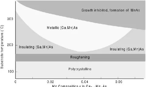
In the (𝐺𝑎, 𝑀𝑛)𝐴𝑠 compound 𝑀𝑛 provides both localized spins and carriers (holes) due to its acceptor nature. A schematic phase diagram of MBE growth is depicted in Fig. 3.2. Clear RHEED oscillations are observed at the initial growth stage (even without 𝑀𝑛), which indicate the growth mode to be two dimensional [5, 6]. This phase diagram shows the tendencies of physical properties vs. growth parameters; however recently it is possible to grow metallic films with 𝑀𝑛 contents of at least 𝑥 = 0.08 [see Chapter 1]. When 𝑇𝑠 is lowered, more compensating defects (Section 3.5) come into play and the 𝐺𝑎1−𝑥𝑀𝑛𝑥𝐴𝑠 layers are insulating. At even lower growth temperatures roughening of the sample occurs, and eventually the 𝐺𝑎1−𝑥𝑀𝑛𝑥𝐴𝑠 films become polycrystalline. When the growth temperature is too high, segregation of 𝑀𝑛𝐴𝑠 clusters occurs at the sample surface, thus inhibiting the incorporation of 𝑀𝑛 in the semiconductor matrix. Metallic 𝐺𝑎1−𝑥𝑀𝑛𝑥𝐴𝑠 films are ferromagnetic, while the highest Curie temperatures are found for samples with the lowest resistivity. Ferromagnetism can even be observed in insulating samples [8, 9].
Fig. 3.2. Schematic phase diagram showing the relation between growth parameters (substrate temperature and 𝑀𝑛 concentration) and the properties of (𝐺𝑎, 𝑀𝑛)𝐴𝑠 grown by MBE [7].
Normally, either a 𝐺𝑎𝐴𝑠 buffer layer or a 𝐼𝑛1−𝑥𝑀𝑛𝑥𝐴𝑠 buffer layer is grown before growth of 𝐺𝑎1−𝑥𝑀𝑛𝑥𝐴𝑠. 𝐺𝑎𝐴𝑠 is grown at low temperatures (𝐿𝑇) and has the same crystal structure, except that 𝐿𝑇 − 𝐺𝑎𝐴𝑠 layers typically contain up to 2% excess 𝐴𝑠, which results in a lattice expansion of the order of 0.1%. As mentioned earlier, the amount of point defects in these 𝐿𝑇 layers depends on the growth temperature, and consequently this holds as well as for the lattice parameters.
The 𝐺𝑎1−𝑥𝑀𝑛𝑥𝐴𝑠 growth can be started by simply commencing the 𝑀𝑛 beam during the low-temperature 𝐺𝑎𝐴𝑠 growth and keeping substrate temperature (𝑇𝑠) constant at 250° and ideally all 𝑀𝑛 atoms randomly substitute 𝐺𝑎 atoms (𝑀𝑛𝐺𝑎) in the zinc blend structure of 𝐺𝑎𝐴𝑠. Although the properties of grown 𝐺𝑎1−𝑥𝑀𝑛𝑥𝐴𝑠 do depend on growth parameters such as 𝐴𝑠 overpressure and 𝑇𝑠 [10, 11], as long as the established growth procedure is followed, the properties of 𝐺𝑎1−𝑥𝑀𝑛𝑥𝐴𝑠 films are reproducible; for example, for a given 𝑀𝑛 concentration 𝑥, the ferromagnetic transition temperature 𝑇𝑐 can always be maintained in the range of 2000𝑥 ± 10 𝐾. The surface reconstruction of 𝐺𝑎1−𝑥𝑀𝑛𝑥𝐴𝑠 is (1 × 2) during and after growth. When the 𝑀𝑛 flux or the substrate temperature or both are too high, a
RHEED pattern indicative of the appearance of the 𝑀𝑛𝐴𝑠 (𝑁𝑖𝐴𝑠 −structure) second phase
on the surface emerges. Maximum 𝑥 so far obtained is about 0.07, above which surface segregation occurs even at low-growth temperature. The lattice constant 𝑎 of 𝐺𝑎𝑀𝑛𝐴𝑠 is larger than that of 𝐺𝑎𝐴𝑠 (𝑎𝐺𝑎𝐴𝑠 =5.65325 Å) and increases with increasing 𝑀𝑛 content [7]. Since 𝐺𝑎1−𝑥𝑀𝑛𝑥𝐴𝑠 grows pseudomorphic on 𝐺𝑎𝐴𝑠 [12, 13, 14], the 𝐺𝑎1−𝑥𝑀𝑛𝑥𝐴𝑠 layer is under compressive biaxial strain with 𝜖𝑥𝑥 = 𝜖𝑦𝑦 = 𝑎𝐺𝑎𝐴𝑠 − 𝑎 𝑎 of the order of minus a few tenths of a percent. Due to dependency on the 𝑀𝑛 concentration one might expect that the 𝐺𝑎1−𝑥𝑀𝑛𝑥𝐴𝑠 lattice constant follows Vegard's law, which states a linear relationship between the concentration of the substitute element and the size of the lattice parameters:
𝑎 = 1 − 𝑥 𝑎𝐺𝑎𝐴𝑠 + 𝑥𝑎𝑀𝑛𝐴𝑠 [3.1] where 𝑎𝑀𝑛𝐴𝑠 is the lattice parameters of the hypothetical zinc-blende 𝑀𝑛𝐴𝑠. This increase of 𝑎 proportionally to 𝑥 occurs because 𝐺𝑎1−𝑥𝑀𝑛𝑥𝐴𝑠 has an intrinsic lattice constant that is larger than that of 𝐺𝑎𝐴𝑠. However, the lattice constant of 𝐺𝑎1−𝑥𝑀𝑛𝑥𝐴𝑠 at a given 𝑀𝑛 content, and therefore as well lattice constant for the hypothetical 𝑀𝑛𝐴𝑠 zinc-blende phase, strongly depend on the growth conditions. Moreover, using density-functional theory (DFT)
calculations Mašek et al. [15] have predicted that increase in lattice constant due to substitutional 𝑀𝑛𝐺𝑎 is minimal, and that the increase in 𝑎 is mainly induced by the 𝐴𝑠𝐺𝑎 and 𝑀𝑛𝐼 point defects (see Section 3.5). They found that the lattice constant is given by:
𝑎 𝑥𝑆, 𝑥𝐴, 𝑥𝐼 = 𝑎𝐺𝑎𝐴𝑠 + 0.02𝑥𝑆+ 0.69𝑥𝐴+ 1.05𝑥𝐼 Å [3.2] where 𝑥𝑆, 𝑥𝐴 and 𝑥𝐼 denote the 𝑀𝑛𝐺𝑎, 𝐴𝑠𝐺𝑎 and 𝑀𝑛𝐼 concentrations, respectively. On the assumption that concentrations of both 𝐴𝑠𝐺𝑎 and 𝑀𝑛𝐼 defects are correlated with the 𝑀𝑛 content, or with the (optimal) growth temperature, eq. [3.2] can be used to explain the apparent Vegard's law behavior.
3.3. Electronic properties
𝐺𝑎𝐴𝑠 is a direct band gap semiconductor with an energy gap 𝐸𝑔 = 1.42 𝑒𝑉 at 300𝐾. When magnetic impurities like 𝑀𝑛 are incorporated in a semiconductor their magnetic and transport properties will depend on the positions of the energy levels corresponding to the magnetic levels with respect to the energy bands of the host semiconductor. Together with the on-site correlation energy 𝑈, this position of the 𝑀𝑛 energy levels will determine the charge and spin state of the 𝑀𝑛 atom, and whether it will act as a dopant. Isolated 𝑀𝑛 atoms have (𝐴𝑟)3𝑑54𝑠2 electron configuration, and when these atoms are incorporated in a 𝐼𝐼𝐼 − 𝑉 semiconductor, they are expected to substitute the trivalent cation. As the 𝑀𝑛 atom has only two valence electrons, the formation of a hole is expected and at this substitutional position there are three possible electronic ground states for the 𝑀𝑛 impurity: 𝐴0(𝑑4), 𝐴0(𝑑5 + ) (a complex configuration with hole () weakly bound to the 𝑀𝑛 ion) and 𝐴−(𝑑5) [16]. Here, 𝐴0 denotes the state in which the 𝑀𝑛 center is neutral with respect to the 𝐺𝑎𝐴𝑠 background and thus corresponds to a 𝑀𝑛3+ state, while 𝐴− is the “negatively charged” 𝑀𝑛2+ center. The notation in brackets is the electronic configuration of the 𝑑 electrons. In case of 𝐴0(𝑑4), the hole resides in the 𝑀𝑛 3𝑑 shell. In 𝐺𝑎𝐴𝑠 doped with 𝑀𝑛 the 𝐴0(𝑑4), configuration is not observed [17], as due to a strong intra-site Hund coupling a state with five 𝑑 electrons is energetically more favorable, as is the case for 𝐴0(𝑑5 + ) and 𝐴−(𝑑5). In accordance to that, photoemission measurements in 𝐺𝑎1−𝑥𝑀𝑛𝑥𝐴𝑠 [18] reveal an energy level deep (~ 2.7 𝑒𝑉) below the
valence band edge which can be attributed to the 𝑀𝑛 𝑑4 𝑑5 acceptor state [19], i.e. the transformation of the triply ionized ions 𝑀𝑛3+ into 𝑀𝑛2+. As the acceptor state lies under the top of the valence band, the ground state corresponds to the 𝑀𝑛 𝑑5 state. When an 𝐴0(𝑑4), traps an electron tightly in the 3𝑑 shell forming the high spin, 𝑆 = 5 2 , 3𝑑5 configuration, it is negatively charged in respect to the 𝐺𝑎𝐴𝑠 background and can therefore bind the hole in a effective mass acceptor state 𝐴0(𝑑5 + ). The energy of this hydrogen-like state will then be found just above the valence band, where the binding energy of the hole corresponds to the ionization energy of the acceptor. In the low doping range 𝑀𝑛 ions are indeed found to be acceptors with an ionization energy of 112 𝑚𝑒𝑉 [20, 21]. In Fig. 3.3 it is described, from reference [17, 22], the presence of the change of energy gap in the 𝐺𝑎𝑀𝑛𝐴𝑠 respect to 𝐺𝑎𝐴𝑠 with STS technique. Various experimental results indicate that the ground state of the 𝑀𝑛 impurity at low doping concentrations corresponds to the 𝐴0(𝑑5 + ) configuration [16]. Photoemission experiments show that the itinerant holes originating from the 𝑀𝑛 acceptor level mainly have an 𝐴𝑠 4𝑝 −character, and can thus be associated with the host semiconductor valence band [23].
Fig. 3.3. 𝐼 𝑉 curves acquired on the clean 𝐺𝑎𝐴𝑠 surface (solid line) and in the middle of the cross like feature (dashed line) with 3 ∙ 1018 𝑐𝑚 −3 𝑀𝑛 doping level. The simulated position of the flat-band potential 𝑈𝐹𝐵 is indicated by the labeled arrow. Inset displays energy band diagram for the positive sample bias [22].
When the 𝑀𝑛 concentration is increased the acceptor states will start to overlap and the energy level will broaden and form an impurity band. At high 𝑀𝑛 content this impurity band will merge with the 𝐺𝑎𝐴𝑠 valence band, leading to the insulator-to-metal transition as holes are induced in the valence band that can be considered as itinerant. In this case the ground state of some of the 𝑀𝑛 atoms will be 𝐴−(𝑑5), where the hole resides in the valence band and the 𝑀𝑛 ion is in the 3𝑑5 (𝑆 = 5 2 ) configuration. This configuration will also be favored due to the high hole concentrations in the typical doping range of 𝐺𝑎1−𝑥𝑀𝑛𝑥𝐴𝑠, which may lead to screening of the Coulomb potentials of the 𝐴− centers, resulting in a lower ionization energy of the holes [16].
3.4. Magnetic properties
Sharp, square hysteresis loops, indicating a well-ordered ferromagnetic structure, have been measured in the magnetization (𝑀) versus magnetic field (𝐵) curves with 𝐵 applied in the plane of the film measured for several 𝑀𝑛 concentrations [24]. Below 𝑥 = 0.005 no ferromagnetism was detected. The low-temperature saturation magnetization, 𝑀𝑆, of the (𝐺𝑎, 𝑀𝑛)𝐴𝑠 film is given by 𝑀𝑀𝑛 = 𝑁𝑀𝑛𝑔𝜇𝐵𝑆𝑀𝑛, where 𝑁𝑀𝑛 is the nominal 𝑀𝑛 concentration, 𝑔 = 2 the 𝑔2 factor of 𝑀𝑛, 𝜇
𝐵 is the Bohr magneton, and 𝑆𝑀𝑛 the spin of 𝑀𝑛. The possible values for 𝑆𝑀𝑛, as we saw before, are 5 2 for 𝑀𝑛2+ and 4 2 for 𝑀𝑛3+. The measured 𝑀
𝑆 with nominal 𝑥 results between the two [7]. Normally absence of remanence above 𝑇𝑐 of (𝐺𝑎, 𝑀𝑛)𝐴𝑠 confirmed that the concentration of 𝑀𝑛𝐴𝑠 inclusions (𝑇𝑐 = 310 𝐾), if present, is very low. When 𝐵 is applied perpendicular to the (1 0 0) sample surface, an elongated magnetization curve with little hysteresis is obtained, indicating that the easy-axis for magnetization is in the plane. This occurs because (𝐺𝑎, 𝑀𝑛)𝐴𝑠 layers growth on 𝐺𝑎𝐴𝑠 substrate are under compressive strain. Susceptibility 𝜒 of (𝐺𝑎, 𝑀𝑛)𝐴𝑠 films follows the Curie-Weiss form 𝜒 = 𝐶 𝑇 − 𝜃 , where 𝐶 is the Curie constant and 𝜃 the paramagnetic Curie temperature. 𝜃 appears to fall close to 𝑇𝑐. In the absence of carriers, however, 𝜃 becomes negative (−2 𝐾) indicating that the direct
2
A g-factor (also called g-value or dimensionless magnetic moment) is a dimensionless quantity which characterizes the magnetic moment and gyromagnetic ratio of a particle or nucleus.
exchange among 𝑀𝑛 is antiferromagnetic and the ferromagnetic interaction observed in these films are carrier (hole) mediated [25].
Electrical transport measurements as a function of 𝑇 as well as 𝐵 have proven a powerful investigation tool for (𝐺𝑎, 𝑀𝑛)𝐴𝑠 films. The dominant contribution from the anomalous Hall effect in 𝑝 −type (𝐺𝑎, 𝑀𝑛)𝐴𝑠 made it possible to determine the magnetic properties from the magnetotransport measurements. The sheet Hall resistivity 𝑅𝐻𝑎𝑙𝑙 (or the Hall resistivity 𝜌𝐻𝑎𝑙𝑙) in magnetic materials is expressed as 𝜌𝐻𝑎𝑙𝑙 = 𝑅𝐻𝑎𝑙𝑙𝑑 = 𝑅0𝐵 + 𝑅𝑆𝑀 where 𝑅0 is the ordinary (normal) Hall coefficient, 𝑅𝑆 the anomalous Hall coefficient, 𝑑 the sample thickness, and 𝑀 the magnetization of the sample. Separate measurements showed that 𝑅𝑆 is proportional to 𝑅𝑠𝑒𝑒𝑡, indicating that the skew scattering is responsible for the anomalous term [26], and thus 𝑅𝑆 = 𝑐𝑅𝑑 𝑠𝑒𝑒𝑡 where 𝑐 is a temperature-independent constant. Because of the high-hole concentration, the anomalous Hall term is the dominant term even up to room temperature. This allows one to determine 𝑀 of the sample from 𝑅𝐻𝑎𝑙𝑙 (𝑀 ~ 1 𝑐 𝑅𝐻𝑎𝑙𝑙 𝑅𝑠𝑒𝑒𝑡). Fig. 3.4 shows the temperature dependence of 𝑅𝑠𝑒𝑒𝑡 of six 200 𝑛𝑚 thick (𝐺𝑎, 𝑀𝑛)𝐴𝑠 epitaxial films grown on (𝐴𝑙0.9𝐺𝑎0.1)𝐴𝑠 buffer layer [7]. The temperature dependence of 𝑅𝑠𝑒𝑒𝑡 of samples with intermediate 𝑀𝑛 composition (𝑥 from 0.035 to 0.053) shows that they are on the metal side of the metal-insulator transition whereas low and high 𝑥 samples are on the insulator side.
Fig. 3.4. Temperature dependence of sheet resistivity 𝑅𝑠𝑒𝑒𝑡 of (𝐺𝑎, 𝑀𝑛)𝐴𝑠 thin films grown on (𝐴𝑙0.9𝐺𝑎0.1)𝐴𝑠 buffer layers. Samples with intermediate composition (0.035 − 0.053) are metallic [7].
At 𝑇𝑐, all samples show a hump in 𝑅𝑠𝑒𝑒𝑡 − 𝑇 curves, which is most pronounced in metallic samples. This anomalous temperature dependence is most probably due to the critical scattering, in which carriers are scattered by magnetic fluctuation through exchange interaction.
Several models have been put forward to explain the origin of ferromagnetism in 𝐺𝑎𝑀𝑛𝐴𝑠. In principle various mechanisms for the hole mediated exchange coupling in 𝐺𝑎1−𝑥𝑀𝑛𝑥𝐴𝑠 are possible like double exchange, Zener mechanism, RKKY interaction. For further information about these mechanism see ref. [27, 28, 29]. A brief discussion of these models is reported below. Numerous experimental results indicate that the ferromagnetic interaction in dilute magnetic semiconductors is mediated by the charge carriers, which are in most cases valence band holes. The antiferromagnetic superexchange in these samples can be overcompensated by ferromagnetic interactions mediated by band holes. The magnetic interaction among 𝑀𝑛 has been shown to be antiferromagnetic in 𝑛 −type 𝐼𝑛1−𝑥𝑀𝑛𝑥𝐴𝑠 [30] and in fully carrier compensated 𝐺𝑎1−𝑥𝑀𝑛𝑥𝐴𝑠 using 𝑆𝑛 as a donor [31], indicating the critical role of the holes for the magnetic coupling. The hole mediated origin of the ferromagnetism in 𝐺𝑎1−𝑥𝑀𝑛𝑥𝐴𝑠 is further evidenced by the correlation between its transport and magnetic properties. The ferromagnetic properties of diluted magnetic semiconductors result from the presence of a spin-dependent interaction between the electrons or holes in the 𝑠𝑝 bands of the semiconductor host and electrons residing on the 𝑑 shells of the magnetic impurities [32], as illustrated schematically in Fig. 3.5.
Fig. 3.5. Schematic illustration of the hole mediated exchange interaction in diluted magnetic semiconductors. A long range ferromagnetic interaction of the 𝑀𝑛 spins results from a strong antiferromagnetic coupling of the itinerant or weakly bound holes to the localized spins.
This interaction assumes a form of the Heisenberg exchange coupling, ℋ𝑒𝑥 = − 𝐽𝑒𝑥 𝑠 ∙ 𝑆 where 𝐽𝑒𝑥 describes the strength of the interaction between the carrier spin 𝑠 and the transition-metal spin 𝑆 . If 𝐽𝑒𝑥 is positive the lowest energy state corresponds to a parallel spin alignment, while an antiferromagnetic alignment is favored when 𝐽𝑒𝑥 is negative. In
𝐺𝑎1−𝑥𝑀𝑛𝑥𝐴𝑠, the hybridization of the valence band holes (with 𝑝 −orbital character) and the 𝑀𝑛 𝑑 states that results in spin-dependent interaction, the so called kinetic exchange, which is characterized by a rather large exchange energy 𝐽𝑝𝑑 = −1 𝑒𝑉 [32]. The negative sign of 𝐽𝑝𝑑 reflects an antiferromagnetic coupling between the hole spin and the localized 𝑀𝑛 spin. These 𝑠𝑝 − 𝑑 exchange couplings give rise to a spin-splitting of the bands proportional to the sample magnetization. The antiferromagnetic coupling between the hole spin and the localized 𝑀𝑛 spin leads to a long range ferromagnetic coupling between neighboring 𝑀𝑛 spins (see fig. 3.5), which eventually results in a ferromagnetic state at low temperatures.
3.5. Defects
Although there is some lattice mismatch between the 𝐺𝑎1−𝑥𝑀𝑛𝑥𝐴𝑠 layer and the 𝐺𝑎𝐴𝑠 substrate, 𝐺𝑎1−𝑥𝑀𝑛𝑥𝐴𝑠 can be grown pseudomorphically (fully strained), so no dislocations are formed at the interface. However due to the low temperatures which are required to grow 𝐺𝑎1−𝑥𝑀𝑛𝑥𝐴𝑠 (see fig. 3.2), point defects are inevitable and the concentration of (double) donor-like defects can be as high as 30% of the 𝑀𝑛 content 𝑥. There are three main types of defects in 𝐺𝑎1−𝑥𝑀𝑛𝑥𝐴𝑠: 𝐴𝑠 antisite, 𝑀𝑛 Interstitials and 𝑀𝑛𝐴𝑠 precipitates.
As antisites (𝐴𝑠𝐺𝑎) are defects formed when 𝐴𝑠 atoms occupy a 𝐺𝑎 site in the zinc blend structure. These defects are well established in 𝐺𝑎𝐴𝑠 layers grown by low temperature (LT) MBE. In the LT-regime both the surface mobility of 𝐴𝑠 molecules and the 𝐴𝑠 desorption rate are reduced, so that part of the excess As is non-stoichiometrically incorporated into the lattice and forms 𝐴𝑠𝐺𝑎 as the dominant 𝐴𝑠 −related defect [33, 34]. It is therefore not surprising that these defects play an important role in the electronic properties of 𝐺𝑎1−𝑥𝑀𝑛𝑥𝐴𝑠. 𝐴𝑠𝐺𝑎 act as double donors [35], and one 𝐴𝑠𝐺𝑎 may thus compensate the holes induced by two 𝑀𝑛𝐺𝑎. As the ferromagnetism in DMS materials is hole-mediated, a reduction of the hole concentration affects both the electronic and magnetic properties of 𝐺𝑎1−𝑥𝑀𝑛𝑥𝐴𝑠. The amount of 𝐴𝑠𝐺𝑎 decreases with increasing temperature. 𝐺𝑎1−𝑥𝑀𝑛𝑥𝐴𝑠 layers with low 𝑀𝑛 content, which can be grown at higher
![Fig. 4.20. Schematic illustration of the assumptions used in the single scattering cluster (SSC) model, with various important quantities defined [28]](https://thumb-eu.123doks.com/thumbv2/123dokorg/7605551.114800/86.892.247.634.126.508/schematic-illustration-assumptions-scattering-cluster-various-important-quantities.webp)