Università del Piemonte Orientale “Amedeo Avogadro”, Alessandria
Dipartimento di Scienze e Innovazione Tecnologica (DiSIT)
Advances in Sensors: The Enabling Roles
of Photocatalysis, Polymer Brushes and
Exotic Characterization Approaches
Guido Panzarasa
Advisor: Dr. Katia Sparnacci
Ph.D. Thesis in Chemical Sciences
3
Table of Contents
General Abstract
(p. 5)Introduction
(p. 7)I. Photocatalytic Lithography: a Powerful Technique for the
Patterning of Polymer Brushes and Nanoparticles
1. Patterning of Polymer Brushes Made Easy Using Titanium Dioxide: Direct and Remote Photocatalytic Lithography (p. 10)
2. SERS-Active Patterns Obtained by Photocatalytic Shaping of Self-Assembled Silver Nanoprisms (p. 44)
II. Polymer Brushes: Advanced Applications and Innovative
Characterization
3. Grafted-From Polymer Brushes Make Silicon Wafer Electrochemically Responsive (p. 61)
4. Positron Annihilation Spectroscopy: A New Frontier for Understanding Nanoparticle-Loaded Polymer Brushes (p. 91)
4
III. Self-Cleaning Properties in Engineered Sensors for the
Electroanalytical Detection of Catecholamine Neurotransmitters
5. Developing an Efficient, Self-Cleaning Device for the Electroanalysis of Catecholamine Neurotransmitters (p. 125)
6. Self-Cleaning Electrochemical Sensors, Part I: Towards Clinical Applications (p. 158) 7. Self-Cleaning Electrochemical Sensors, Part II: A Proof-of-Concept for On-Field
Applications (p. 182)
Conclusion and Perspectives
(p. 200)Appendix A – Polymer Brushes
(p. 203)Appendix B – Titanium Dioxide and Photocatalysis
(p. 211)Appendix C – General Procedures
(p. 215)Collaborations
(p. 220)5
General Abstract
The work described in this Thesis is highly interconnected and related to applied surface science, polymer chemistry and nanotechnology. For the sake of clarity, this work has been divided in three Sections with subsequent division in Chapters.
Section I is dedicated to the application of photocatalytic lithography to the patterning and
modification of self-assembled monolayers, polymer brushes and nanoparticles. Here, the first example of polymer brushes patterning based on photocatalytic lithography is reported.
Section II is about the characterization of polymer brushes using exotic techniques such as
positron annihilation spectroscopy (PAS) and electrochemistry. The most relevant features described are: the first report about the application of PAS to the study of polymer brushes and of their composites with nanoparticles, and the first report on the electrochemical properties of silicon wafer coated with grafted-from functional polymer brushes.
In Section III an innovative self-cleaning electroanalytical sensor for the detection of catecholamine neurotransmitters is presented. The relevance of this work can be best described by referring to the highlights received in Chemistry World and Scientific American. There are three Appendices: Appendix A introduces polymer brushes and Appendix B deals with titanium dioxide photocatalysis, while in Appendix C the general synthetic procedures reported throughout this Thesis are described in detail.
6
Keywords
Surface science, Nanotechnology, Titanium dioxide, Photocatalysis, Self-assembly, Lithography, Patterning, Polymer brushes, Controlled radical polymerization, SI-ATRP, Silver nanoparticles, SERS, Positron Annihilation Spectroscopy, Electrochemistry, Self-cleaning, Catecholamine neurotransmitters, Sensors.
7
Introduction
Sensing the difference
Sensors are everywhere.
They are not only companions of our daily life: they are essential part of us and, more broadly, of all living beings. The sense of taste, of smell, of touch, of view, of hearing are all products of complex sensing systems shaped by Nature during eons of evolution. Sensors and sensor systems are vital to our awareness of our surroundings and provide safety, security and surveillance as well as enable monitoring of our health and environment. No mystery that they are so important, after all.
A sensor is defined as a device able to give a response, of qualitative and/or quantitative nature, when subjected to a proper stimulus.
A transformative advance in the field of sensor technology has been the development of smart sensor systems. The definition of a smart sensor may vary, but typically, a smart sensor is the combination of a sensing element with processing capabilities provided by a microprocessor. That is, smart sensors are basic sensing elements with embedded intelligence. The sensor signal is fed to the microprocessor, which processes the data and provides an informative output to an external user. The innumerable applications of such systems are apparent. The incorporation of sensors into textiles (wearable sensors) and
8
eventually into living bodies for e.g. real-time monitoring of vital parameters is of special relevance in this context.
One major implication of smart sensor systems is the use of robust and reliable sensing devices. It could appear to be trivial, but even the most intelligent system is completely useless if its sensing core doesn’t work properly. For this reason, it is of paramount importance to develop highly efficient sensing platforms with self-calibrating, self-healing, self-compensating and self-cleaning properties. This is one of the most challenging and actual field of research, which benefited much from the “nanotechnology revolution”, generating high promises especially for the development of miniaturized devices. This broad field crosses many different disciplines ranging from chemistry to physics to materials science, with a major role played by surface science.
The scope of this Thesis is to explore three different, although converging, approaches to develop such kind of sensing platforms.
The enabling roles of photocatalysis, polymer brushes and of exotic characterization techniques (such as positron annihilation spectroscopy) to reach this goal are discussed. Theoretical as well as highly applicative results are described, as products of a genuine curiosity-driven approach.
9
I
Photocatalytic Lithography: a Powerful
Technique for the Patterning of Polymer
Brushes and Nanoparticles
10
Chapter 1
Patterning of Polymer Brushes Made Easy
Using Titanium Dioxide: Direct and Remote
Photocatalytic Lithography
ABSTRACT Photocatalytic lithography is demonstrated for the first time as a convenient
technique to achieve patterning of polymer brushes. Both a “direct” and a “remote” approach are studied and both are based on the efficient degradation experienced by organic molecules when exposed to photo-generated reactive oxygen species. In the direct approach, a photoactive titanium dioxide surface, previously functionalized with a suitable initiator of polymerization, is exposed to near-UV light through a contact photomask. On the other hand, in the remote approach irradiation is performed on a generic, initiator-functionalized substrate through a transparent photoactive TiO2 film and a photomask. Selective degradation of initiator molecules only in the zones not covered by the photomask is observed. The resulting pattern is then amplified as polymer brushes with surface-initiated polymerization technique. Features down to 10 μm can be obtained using simple equipment. The process is intrinsically parallel, high-throughput and scalable to wafer size, does not require photoresists nor high-intensity UV sources, making it relatively safe for the operator and powerful for microfabrication purposes. The possibility to obtain positive and negative patterns has been demonstrated using direct photocatalytic lithography, while remote photocatalytic lithography has been successfully coupled with nanosphere lithography.
11
1.1 Introduction
Polymer brushes, dense arrays of surface-tethered polymer chains, are perfect tools for surface engineering. They exhibit excellent robustness and well-organized chain conformation, which endow superior control over several surface properties such as morphology, grafting density and chemical composition [1-3]. Patterned polymer brushes [4,5] are versatile building blocks for micro-fabrication and controlled assembly of small particles [6], sensors/biosensors and actuators [7-15], drug delivery systems [16], electronic devices [17], anti-biofouling coatings [18] and biocompatible scaffolds [19]. In general, they are efficient means to confer smart, stimuli-responsive behavior to surfaces and interphases [20-22].
By a combination of lithographic tools and surface-initiated polymerization (“grafting-from”, as opposed to “grafting to” which relies on adsorption of preformed polymer) [23,24], micro- and nanoscale architectures can be obtained from suitable self-assembled monolayers (SAMs) [25-28]. SAMs are ordered arrays of molecules chemisorbed at a surface [29]. If they are composed by polymerization initiators, polymer chains can grow directly from them. Eventually, if the SAMs are patterned, patterned polymer brushes will be obtained.
The expertise to master patterning [30] is crucial in order to realize devices with applications ranging from biotechnology [31] to electronics [32]. An impressive array of patterning strategies is available. To name a few: colloidal lithography [33,34], micro-contact printing [35,36], electron beam lithography [37], scanning probe [38] or near field lithography [39], conventional photolithography (with the use of photoresists [40,41]) and SAM
12
photolithography [42,43]. The latter typically requires high-intensity UV sources [6,44-46] (e.g. deep-UV, vacuum-UV) [47,48] or highly focused beams (UV-lasers) [49].
There is a significant demand for more affordable and facile lithographic techniques, which should update the present technologies [50] to reliably pattern polymer brushes at the wafer scale [51] with high resolution micrometric and sub-micrometric features. Here we are reporting for the first time about how this challenge can be successfully addressed by taking advantage of photocatalytic lithography [52,53].
TiO2 is one of the major protagonists in nanotechnology. It is inexpensive, non-toxic, its surface is biocompatible and can be functionalized using established chemistries [54]. It is an intrinsic semiconductor whose photochemical and photophysical properties have had great relevance both in fundamental [55,56] and applied research [57,58]. When TiO2 is irradiated with photons of wavelength in the UV region, electron-hole pairs are produced: holes are powerful oxidants, electrons are good reducing agents and both rapidly react with adsorbates [59]. Titanium dioxide is now playing a central role for the engineering of surfaces [60,61], in particular in the field of lithography [53,62]. Here, we report for the first time an improved access to micro-patterned polymer brushes using near-UV light titanium dioxide phocatalytic lithography.
First, transparent and mechanically robust TiO2 anatase films with high photoactivity are deposited on glass and silicon wafer from an acidic TiO2 sol using an electrochemically-assisted technique first reported by the Group of Prof. S. Ardizzone (all the relevant details can be found in Appendix C) [63]. The requirement of common lab instrumentation and the possibility to store and reuse the sol for up to one month makes this process highly appealing, cheap and scalable. In addition, the quality of the TiO2 film is better in terms of
13
smoothness (rms 0.563 nm) compared to those commonly obtained by dip-coating or spin-coating (Figure 1.1) [64]. Film thickness can be increased at will by repeating the deposition cycle [63]. The films showed the typical increase in hydrophilicity upon exposure to 365 nm UV radiation due to enhanced hydroxyl surface termination (generally reported as “surface-induced hydrophilicity” [65]). We exploited this phenomenon to improve chemisorption of the atom transfer radical polymerization (ATRP) initiator (3-(2-bromoisobutyramido)propyl)triethoxysilane (BIB-APTES) [66] on TiO2.
Figure 1.1 Titanium dioxide films deposited on glass: in a) the film high transparency is
evident, in b) XRD analysis shows pure anatase polymorph, with crystallite dimension of ~ 17 nm. c) AFM topography picture (tapping mode).
We use then surface-initiated atom transfer radical polymerization (SI-ATRP), a controlled free radical polymerization process, to amplify the obtained initiator pattern into a polymer brushes pattern [67,68]. Compared to other controlled radical polymerization techniques, ATRP allows to adopt very mild conditions (e.g. polymerization can be conducted at room
14
temperature). Both “conventional” and “activators regenerated by electron transfer” (ARGET) ATRP are used in this study. The latter is selected thanks to improved oxygen tolerance and lower concentration of metal catalyst required [69]. Methyl methacrylate (MMA) is chosen as a standard monomer but any other ATRP-friendly monomer can be used.
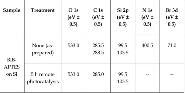
Figure 1.2 Patterned polymer brushes obtained by photocatalytic lithography of
initiator-functionalized substrates. Steps: 1) grafting of the ATRP initiator, 2) pattern formation using either direct (2a) or remote (2b) photocatalytic lithography, 3) pattern amplification using SI-ATRP to obtain 4) the corresponding polymer patterns (4a, 4b).
1.2 Results and Discussion
1.2.1 Direct Photocatalytic Lithography
Direct photocatalytic lithography (Figure 1.3) is achieved by irradiating, with 365 nm near-UV light, a self-assembled monolayer (SAM) of ATRP initiators grafted directly on a titanium dioxide film. A metallic TEM grid deposited the substrate performs as a contact photomask. The resulting pattern is then amplified into polymer brushes by surface-initiated polymerization.
15
Figure 1.3 Patterning of polymer brushes by direct photocatalytic lithography.
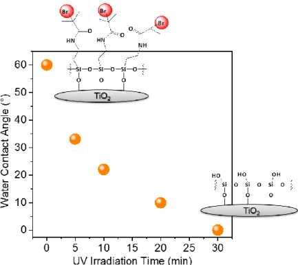
The kinetics of photocatalytic degradation are followed on dedicated substrates by water contact angle measurements (Figure 1.4). The water contact angle for surfaces functionalized with BIB-APTES, stored in the dark, is 75°. After 1 h of irradiation, the θw
decreases to less than 15°.
Figure 1.4 Water contact angle kinetics for the photodegradation of BIB-APTES grafted on
TiO2 exposed to 365 nm-UV light. The most probable structures of the initiator SAM before and after 30 min of irradiation are showed.
16
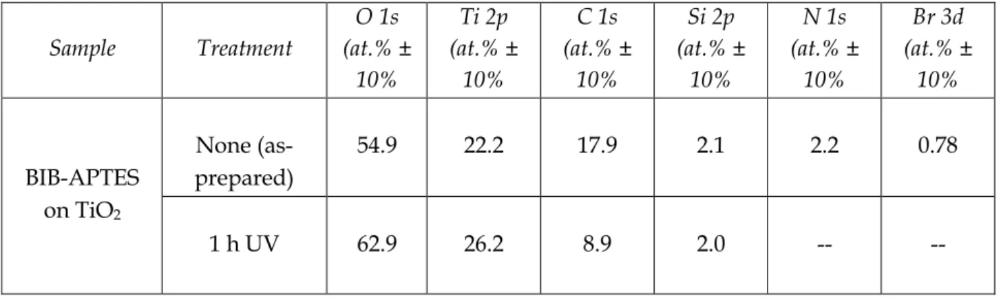
The disappearance of nitrogen and bromine signals from the XPS spectra gave definitive evidence of complete removal of the initiator molecules (Figure 1.5, Tables 1.1 and 1.2). On the other hand, BIB-APTES grafted on surfaces with no photoactivity such as silicon wafer or glass remains unaffected even after 3 h of UV irradiation as confirmed by the unchanged water contact angle and ability to start the growth of polymer brushes. That demonstrates the critical role of TiO2 for the photopatterning of initiator.
Figure 1.5 XPS confirmation of the photocatalytic degradation of grafted initiator. Black line:
before irradiation. Blue line: after 1 h of 365 nm-UV irradiation.
It can be seen, from the relative atomic percentages (Table 1.1), that there is a C:N ratio of about 8:1 for BIB-APTES grafted on TiO2. These values are in good accordance with the 7:1 C:N ratio expected for a uniform SAM of BIB-APTES with each of its three Si–O groups forming a siloxane bond with the –OH-terminated TiO2 surface. Although some molecules may retain ethoxy functional groups on their Si–O tails, an ordered monolayer has formed. The Br 3d signal is apparently underestimated, thus preventing its quantification. However, complete disappearance of both nitrogen and bromine signals after direct photocatalytic lithography confirms the successful degradation of the initiator molecules. Table 1.2 reports the energetic positions of principal peaks. For carbon, signals relating to C–C (285.0 eV) and
17
C=O (288.5) are observed, in accordance with the molecular structure of BIB-APTES. For BIB-APTES on TiO2 after 1 h of UV irradiation a shoulder appears at 286.5 eV which is attributable to –C-OH groups. The position of N 1s peak at 400 eV was assigned to the O=C-N species. The oxygen peak position is dependent on nature of the surface: in this case, it is 530.5 eV. The position of the silicon peak depends on the number of bonded oxygen atoms: 99.5 eV, no bound oxygen atoms; 102.5 eV, three bound oxygen atoms; 103.5 eV, four bound oxygen atoms.
Table 1.1 Atomic composition of BIB-APTES–functionalized surfaces before and after direct
photocatalytic lithography determined by XPS.
Sample Treatment O 1s (at.% ± 10% Ti 2p (at.% ± 10% C 1s (at.% ± 10% Si 2p (at.% ± 10% N 1s (at.% ± 10% Br 3d (at.% ± 10% BIB-APTES on TiO2 None (as-prepared) 54.9 22.2 17.9 2.1 2.2 0.78 1 h UV 62.9 26.2 8.9 2.0 -- --
Table 1.2 Binding energy for the principal elements detected by XPS.
Sample Treatment O 1s (eV ± 0.5) Ti 2p3 (eV ± 0.5) C 1s (eV ± 0.5) Si 2p (eV ± 0.5) N 1s (eV ± 0.5) Br 3d (eV ± 0.5) BIB-APTES on TiO2 None (as-prepared) 530.5 459.0 285.0 288.5 102.5 400.0 71.0 1 h UV 530.5 459.0 285.0 286.5 289.0 102.5 -- --
18
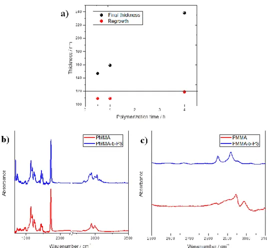
Polymerization of MMA is carried out at 30 °C in a 4:1 v/v methanol-water mixture using a CuBr2/tris(2-pyridylmethyl)amine (TPMA) catalyst activated by an excess of ascorbic acid. Water contact angle measurements (68°, which is consistent with previous wetting experiments with water on PMMA brushes [70]) and FTIR analysis confirm the successful grafting of polymer brushes (Figure 1.6b,c, red line).
Figure 1.6 a) Demonstration of the reinitiation efficiency for PMMA brushes. The straight
line represents the mean thickness h4h for a 4 h-grown PMMA brush. Results indicate very
good macroinitiator efficiency (I ≥ 90 %), i.e. the fraction of the original growing chains capable to restart polymerization. That is defined as 𝐼 = (∆ℎ ℎ4ℎ⁄ ) ∙ 100, where ∆ℎ is the thickness increase after restarting polymerization with MMA. (b) Comparison of FTIR spectra for a poly(methyl methacrylate) (PMMA) brush, thickness 106 ± 1 nm, and for a block copolymer brush obtained by restarting polymerization from PMMA brush with styrene (PS thickness 86 ± 2 nm). Substrate: silicon wafer. Both brushes show characteristic IR absorption spectra with the most pronounced differences occurring in the C–H stretching regions. A strong peak due to C=O stretching at 1730 cm-1 is visible in both spectra. In the
19
PMMA spectrum, the main features are at 2951 cm-1 (CH2 asimmetric stretching and CH3 asimmetric stretching) and at 2996 cm-1 (CH3 of OCH3 asimmetric stretching). In the PMMA-PS block copolymer spectrum, the diagnostic peaks are at 699 cm-1 and 755 cm-1 (wagging of the 5 H of the aromatic ring), 2847 cm-1 (CH2 simmetric stretching), 2927 cm-1 (CH2 asimmetric stretching); the peaks at 2998 cm-1, 3026 cm-1 , 3060 cm-1, 3083 cm-1 are all due to the aromatic C–H stretching). (c) Comparison of FTIR spectra for a poly(methyl methacrylate) (PMMA) brush, thickness 83 ± 1 nm and for a block copolymer brush obtained by restarting polymerization from PMMA brush with styrene (PS thickness 83 ± 2 nm). Substrate: TiO2. Both brushes show characteristic IR absorption spectra with the most pronounced differences occurring in the C–H stretching regions. In the PMMA spectrum, the peaks at 2946 cm-1 (CH2 asimmetric stretching and CH3 asimmetric stretching) and at 2999 cm-1 (CH3 of OCH3 asimmetric stretching) are visible. In the PS spectrum, the peaks at 2849 cm-1 (CH2 simmetric stretching) and at 2918 cm-1 (CH2 asimmetric stretching) can be recognized.
Polymerization on BIB-APTES–functionalized substrates proceeds smoothly, leading to PMMA brushes with thicknesses up to 200 nm depending upon the amount of time allowed for polymerization. The brush thickness is linearly correlated with polymerization time (over at least 8 h) suggesting a good control of the polymerization (Figure 1.7).
Figure 1.7 Evolution of PMMA brushes thickness as a function of the polymerization time.
A deviation from linearity is observed for longer reaction times, which could be explained by increased steric interference to chain growth as polymer brushes grow longer and by the occurrence of irreversible chain termination.
20
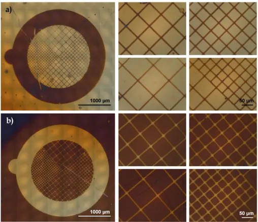
This is confirmed also by the excellent (≥ 90%) re-initiation efficiency showed by the brushes (Figure 1.6a), which allows to perform block-copolymerization. For example, PMMA-b-PS brushes with a poly(styrene) (PS) block up to 80 nm thick are obtained by subsequent polymerization of styrene for 4 h from a PMMA brush as shown by the increase in contact angle (from 68° to 90°, in accordance with literature findings [71]) and FTIR analysis (Figure 1.6, blue line). According to SEM and AFM images, the grid patterns are successfully replicated by polymer brushes onto the TiO2 surface and 10 μm-wide PMMA lines were obtained with very good resolution (Figure 1.8).
Figure 1.8 Polymer brushes patterns obtained after SI-ATRP of patterned initiators: a)
optical microscopy (the inset shows the picture of a typical sample), b,c) scanning electron microscopy, d-f) atomic force microscopy (tapping mode).
21
Patterning of pH-responsive polymer brushes
As already mentioned, peculiar properties arise from polymer brushes with specific structure, making them powerful tools for surface engineering. Examples are control of phase-segregation in response to external stimuli, wetting control, lubrication, adsorption of molecules and particles (including proteins and cells) [72]. Noteworthy, brushes made of polyelectrolytes are able to respond to a wide range of external stimuli such as pH, temperature and ionic strength, which induce structural (e.g. swelling) and chemical (e.g. functional group modification) changes in the individual polymer chain leading to a collective, amplified response of the brushes [73-75]. Poly(2-(dimethylamino)ethyl methacrylate) (PDMAEMA) is one of the most studied pH-responsive polymer for the development of smart surfaces, sensors and actuators [76,77] and for this reason it is chosen here to demonstrate the potential of photocatalytic lithography applied to polymer brushes. After direct photocatalytic lithography of a BIB-APTES initiator SAM on titanium dioxide, polymerization of DMAEMA is performed using conventional ATRP in presence of 5 mol% CuBr2 as added deactivator (see the Specific procedures paragraph for details) [78]. The brushes thickness can be tuned by increasing the polymerization time up to 4 h: the linear increase of thickness as a function of the polymerization time suggests a controlled process (Figure 1.9a).
22
Figure 1.9 Depiction of the polymerization process for PDMAEMA brushes and resulting a)
polymerization kinetics, b) FTIR spectra.
Successful formation of PDMAEMA brushes is confirmed also by FTIR spectroscopy (Figure 1.9b). BIB-APTES–functionalized substrates show only peaks from the –CH2– groups. Extra peaks are visible after DMAEMA polymerization at 2760 cm-1 and 2810 cm-1 (symmetric stretching) and a peak at 2930 cm-1, associated with C–H vibration modes of –CH3 of the tertiary amine groups –N(CH3)2 [79-81].
Optical microscopy and scanning electron microscopy are used to examine the pattern quality of the obtained brushes and the resolution attained: the images reveal well defined patterns (ca. 10 micron-width) exactly as those observed for PMMA brushes, demonstrating the effectiveness of photocatalytic lithography (Figure 1.10).
23
Figure 1.10 a) Optical microscopy and b,c) SEM images of patterned PDMAEMA brushes.
PDMAEMA is a weak polybase with pKa ca. 7, thus its tertiary amine group is protonated at pH < 7 and deprotonated at pH > 7 [82]. Protonation introduces electrostatic charges, which cause the chains to repel each other and swell by absorption of water, so pH changes are accompanied by changes in the brushes hydrophilicity which can be easily followed by water contact angle measurements. The brushes (water contact angle ca. 55°) can be made more hydrophilic (ca. 14°) or less hydrophilic (ca. 60°) by simple immersion in acid or base solutions, respectively. This behavior is completely reversible and can be easily appreciated for micropatterned samples (Figure 1.11).
Figure 1.11 The pH-responsive behavior of PDMAEMA brushes is demonstrated by
24
Positive vs Negative Patterns obtained using sacrificial SAMs
In the previous paragraphs, the described pattern was the positive replica of the photomask. However, here we demonstrate that using a sacrificial SAM it is possible to obtain the negative equivalent pattern.
First of all, an ATRP-inert alkylsilane is used to form a self-assembled monolayer on titanium dioxide. To this end, an optimized chemical vapor deposition (CVD) procedure is used (see Appendix C for details) [83]. Then, the SAM is patterned using direct photocatalytic lithography. As discussed before, the exposed zones are free from contamination and are thus prone to be re-filled with another SAM, in this case of an initiator of polymerization such as BIB-APTES. After SI-ATRP, the corresponding negative pattern made of polymer brushes is successfully achieved, as judged by optical microscopy (Figure 1.12) and atomic force microscopy (Figure 1.13).
Figure 1.12 Optical microscopy images of a) positive and b) negative patterns of polymer
25
Figure 1.13 AFM images (2D, 3D reconstruction and profiles) of positive and negative
patterns (grids vs squares) of polymer brushes obtained without and with the use of a sacrificial monolayer, respectively.
The quality of the first SAM is of paramount importance to reduce the risk of spurious polymerization due to the formation of islands during deposition of initiator: the sacrificial SAM must be tightly packed and homogeneous. CVD of Silres1701 proved to be the most
26
successful approach to reach this goal. For example, a sacrificial SAM made of octadecyltrimethoxysilane deposited from toluene with the conventional approach was unsuccessful.
This problem could be overcame using catechol-derived initiators (Scheme 1.1), because they not only have high affinity towards the clean oxide surface but also allow the use of solvents such as water (which are orthogonal towards hydrophobic brushes) [84].
Scheme 1.1 Example of a dopamine-derived ATRP initiator and its attachment to a TiO2
surface through its catechol moiety.
1.2.2 Remote Photocatalytic Lithography
Direct photocatalytic lithography could play a crucial role for innovation in the field of polymer brushes micro-lithography. Nevertheless, the need of a TiO2 layer or, in general, of a photoactive substrate is limiting for many applications. Notwithstanding the smoothness, the transparency, the hardness and the biocompatibility of the titania layer, its
27
photocatalytic properties could not be desired for some applications. In addition, it could be necessary to graft the brushes directly onto a specific surface or onto substrates that cannot withstand a high temperature (ca. 500 °C) thermal treatment, which is needed for the development of titania photoactivity. We found in remote photocatalysis (Figure 1.14) a powerful solution for this general problem.
Figure 1.14 Patterning of polymer brushes by remote photocatalytic lithography.
The Group of A. Fujishima for first reported that the photooxidation of organic molecules could occur not only on the surface of titanium dioxide but also on substrates placed at considerable distances (up to 500 μm) from it [65,85]. The mechanism of remote photocatalysis has been highly controversial until Kubo et al. [86] demonstrated that H2O2 molecules, which are generated at the photocatalyst surface from adsorbed water and oxygen molecules, migrate in the surrounding atmosphere and are cleaved to HO• radicals in the illuminated areas of the target surface (Figure 1.15). Such mechanism is particularly useful to explain the high pattern resolution obtained by us. Highly oxidative radical species form only in the irradiated areas, avoiding lateral oxidation due to migration [87,88].
28
Figure 1.15 Mechanism of remote photocatalytic lithography.
Numerous reports are available on the remote oxidation not only of organic contaminants, alkylsiloxane and thiol SAMs, but also of polymers and metals [89,90]. Here, for the first time, we describe the successful application of remote photocatalytic lithography for the realization of patterned polymer brushes. This is a potentially universal approach, able to generate high resolution patterns on any kind of substrate. In order to obtain a good resolution, avoiding effects connected to the titania substrate morphology and light scattering ability, the quality of the photoactive layer is critical. Again, electrochemically-assisted titania deposition films gave high performance in terms of transparency and smoothness. Remote photocatalytic patterning was performed by irradiating with 365 nm UV light BIB-APTES–functionalized silicon substrates through our titania-coated glass, pre-cleaned by UV irradiation for 1 h, using a 100 μm-thick Teflon spacer. Micropatterning was achieved using a TEM grid and patterns were amplified with PMMA brushes, as already discussed for direct photolithography. Water contact angle decreased from 70° to 33° after
29
2 h of irradiation of the initiator-functionalized substrate. In addition, as for the direct approach, XPS showed complete disappearance of the bromine signal along with the nitrogen signal (Tables 1.3 and 1.4). The discussion of the XPS data is the same for BIB-APTES–functionalized titania. The C:N ratio of 9:1 is indicative of good SAM quality. The only difference compared to TiO2 is the position of the oxygen peak, which depends on the surface nature: 530.5 eV for TiO2, 533.0 eV for SiO2.
Table 1.3 Atomic composition of BIB-APTES–functionalized surfaces before and after remote
photocatalytic lithography determined by XPS.
Sample Treatment O 1s (at.% ± 10% C 1s (at.% ± 10% Si 2p (at.% ± 10% N 1s (at.% ± 10% Br 3d (at.% ± 10% BIB-APTES on Si None (as-prepared) 38.0 24.6 34.5 2.6 0.33 5 h remote photocatalysis 49.6 4.9 45.5 -- --
Table 1.4 Binding energy for the principal elements detected by XPS. Sample Treatment O 1s (eV ± 0.5) C 1s (eV ± 0.5) Si 2p (eV ± 0.5) N 1s (eV ± 0.5) Br 3d (eV ± 0.5) BIB-APTES on Si None (as-prepared) 533.0 285.5 288.5 99.5 103.5 400.5 71.0 5 h remote photocatalysis 533.0 285.0 99.5 103.5 -- --
30
A kinetic investigation is carried out to determine the optimum time necessary to develop a pattern of good quality (Figure 1.16). Although a well-resolved pattern can be obtained after 3 h of irradiation, the best pattern resolution is achieved with an irradiation time of 5 h (Figure 1.17).
Figure 1.16 Optical microscopy images of the pattern evolution of remote photocatalytic
lithography on silicon. For a UV irradiation time of 1.5 h the photomask is clearly replicated with 120 nm-thick PMMA brushes but the internal microstructure is barely visible, also the surrounding surface is heavily stained with polymer (thickness ca. 39 nm). After 2 h, the exposed surface is completely free from polymer and after 2.5 h the pattern replica is completely developed. The resolution of the latter is improved after 3 h of irradiation. The blue color of brushes is due to optical effects.
31
Figure 1.17 Patterning by remote photocatalytic lithography of initiators and subsequent
SI-ATRP. a,b) Optical microscopy and c) scanning electron microscopy of the patterned PMMA brushes obtained on silicon.
Patterning of functional polymer brushes for the development of silicon
wafer-based electrochemical devices
Remote photocatalytic lithography is successfully applied to modify silicon wafer electrodes with different patterns of polymer brushes to perform electrochemical experiments. This work is described in detail in Chapter 3 (Figure 1.18).
Figure 1.18 Polymer brushes can make silicon wafer electrochemically responsive, making
32
Coupling remote photocatalysis with nanosphere lithography
Nanosphere lithography employs self-assembled arrays of nano- or microspheres, typically made of polymer or silica, as lithographic and/or evaporation masks. Due to the very low size of the particles, nanoscale features such as arrays of dots and other features can be fabricated in an economical way [91].
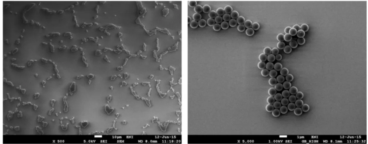
Here we coupled remote photocatalysis with nanosphere lithography to achieve nanoscale patterning of polymer brushes. First, a 1%m/V ethanol suspension of poly(styrene) particles (mean diameter 1 μm, prepared by dispersion polymerization. For details see the Specific procedures section) is spread on the surface of a BIB-APTES–functionalized silicon substrate. Particle self-assembly is then obtained by means of spin-coating (2000 rpm, 500 rpm s-1, 20 s). A sparse particle array is generated, due to the scarce affinity of the nanoparticles towards the surface (Figure 1.19). Typical protocols for the self-assembly of particles are described for highly hydrophilic surfaces [92], in which surface tension effects can drastically help the formation of ordered arrays. In our case, surfactants such as Triton X-100 have been tried to improve the assembly process but without relevant results.
Figure 1.19 Scanning electron microscopy images of the particle arrays generated on
33
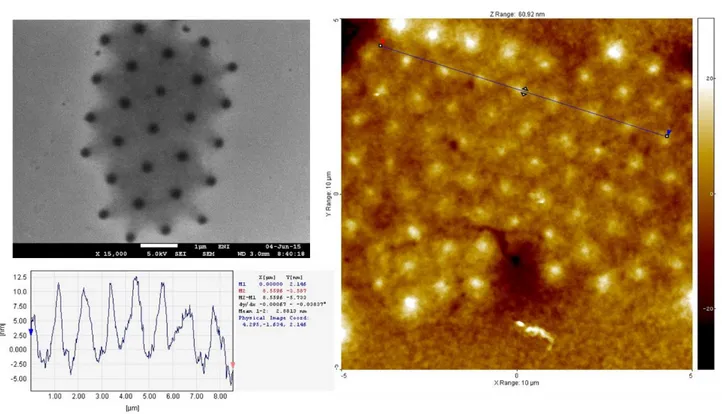
The resulting particle arrays are subjected to remote photocatalytic lithography for 2.5 h according to the procedure described in the previous paragraph. The particles are then removed simply by sonication in ethanol for 5 minutes and the substrates are dried under nitrogen. The obtained pattern is eventually amplified with PMMA brushes (polymerization time: 4 h) using the SI-ATRP protocol described in the Specific procedures paragraph. Figure 1.20 shows the morphology of the resulting patterns.
Figure 1.20 SEM and AFM images of the patterns obtained after 2.5 h of remote
photocatalytic lithography coupled to nanosphere lithography and amplification by SI-ATRP.
From the morphological analysis it can be deduced that, after SI-ATRP, arrays of polymer brushes shaped as conical pillars emerging from a polymer “carpet” are obtained. We hypothesize that this peculiar morphology would originate from an anisotropic, gradient-like etching due to the diffusion of photocatalytically-generated ROS under the particles.
34
According to Scheme 1.2, pillars would arise from the zones where the particles actually touch the substrate, efficiently screening the underlying initiator molecules from the etching action of ROS, while the “carpet” would originate from inter-particle spaces.
Scheme 1.2 Proposed etching processes leading to the formation of polymer pillars and
carpets as a result of remote photocatalysis coupled to nanosphere lithography.
1.3 Conclusion
The growing excitement in the field of polymer brushes and the proved request for efficient patterning strategies urge the introduction of facile and low-cost methods to develop such architectures. Here, we discussed for the first time the use of photocatalytic lithography for making patterned polymer brushes, clearly showing how innovative this approach could be. Titanium dioxide film with high photoactivity are employed to selectively degrade initiators of polymerization under near-UV irradiation using a simple contact photomask and the obtained patterns were replicated by SI-ATRP. Access to negative patterns was demonstrated through the use of sacrificial SAMs.
35
While direct photocatalytic lithography could be obtained only on the surface of a titania layer, the remote approach allowed to achieve photocatalytic patterning on virtually any kind of substrate thanks to the migration of oxidizing species from a TiO2 interface. Both approaches lead to sharp edges and high line resolution. The remote approach is especially relevant being a general, non-invasive and high-throughput lithographic technique. We also demonstrated the successful coupling of remote photocatalysis with nanosphere lithography to obtain arrays of pillars made of polymer brushes. The obtained results are even more relevant considering that even cheap, conventional glass (with a significant inner filter effect towards UV radiation) instead than expensive quartz can be used as a support for titanium dioxide films used to perform photocatalysis experiments.
Our process can be scaled up to the wafer scale, with the future final goal to design controlled areas with different functionalities, useful for applications e.g. in microfluidics and for the development of cell-responsive surfaces.
1.4 Specific procedures
Materials: All the chemicals, unless otherwise stated, were reagent grade, purchased from
Aldrich and used as received. Monomers were filtered through an inhibitor-remover column and stored at –18 °C until use. Silicon (100) wafers, single-polished, n type, phosphorus doped, 3 – 6 (Ω cm), with a native oxide layer ca. 1.5 nm thick, were purchased from Ultrasil Corporation. Cleaning and activation of TiO2 films is accomplished using a Spectroline crosslinker equipped with 254 nm UV lamps. Photocatalytic patterning was achieved using a Jelosil HG500 halogen lamp (refer to Appendix C for details).
Characterization methods: Thickness is measured using a Filmetrics F20 reflectometer.
Each value is the average of at least three measurements performed on different spots of a same sample. Water contact angle analyses are performed using a Krüss Easy Drop
36
Standard with DSA1 software. A 3 μL-drop of HPLC-grade water is deposited and the contact angle measured after 5 s. Each value is the average of at least three measurements performed on different spots of a same sample. Atomic force microscopy (AFM) pictures are acquired on an Ntegra Aura AFM (NT-MDT) device in tapping mode, with NSC35/AIBS tips (μmasch). Scanning electron microscopy (SEM) was performed using a Jeol JSM 7600f Schottky Field Emission Scanning Electron Microscope; to facilitate imaging samples were deposited on conducting carbon tape. X-ray photoelectron spectroscopy (XPS) analyses were performed by a PHI-5500 – Physical Electronics spectrometer, equipped with a monochromatized source with aluminum anode (Kα = 1486.6 eV) operating at a 200 W of applied power. Samples were placed in UHV (10-9 Torr) and irradiated with 200 kV X-rays, survey scans were recorded at a 23.50 eV pass energy, 0.2 s time per step and 0.5 eV energy-step. XPS spectra were collected at takeoff angles of 45°. The analysis area was 0.8 mm2 and the depth was within 10 nm. The spectrometer was calibrated assuming the Ag(3d 5/2) binding energy (BE) at 368.3 eV with respect to the Fermi-level and the measured full width half maximum (FWHM) was 0.46 eV. The quantitative analysis data were reported as atomic percentage of elements and the normalization was performed without including hydrogen. Optical microscopy images and high resolution FTIR spectra were acquired using a Nicolet™ iN™10 Infrared Microscope in transmittance (for silicon samples) or reflectance (for titania samples) mode, with a liquid nitrogen-cooled MCT detector (spectral range 4000 - 675 cm-1, resolution 4 cm-1, aperture 150 x 150 μm).
Background (500 scans) was collected before each sample (1000 scans) from cleaned silicon or titanium dioxide. Baseline correction was performed automatically by the acquisition software.
TITANIUM DIOXIDE FILM DEPOSITION
Refer to Appendix C
SYNTHESIS OF THE ATRP INITIATOR (BIB-APTES)
Refer to Appendix C
GRAFTING OF THE BIB-APTES INITIATOR
37
SURFACE-INITIATED POLYMERIZATION
SI-ARGET ATRP of methyl methacrylate (MMA)
In a nitrogen-purged Schlenk flask 0.021 g (~ 0.07 mmol) of tris(2-pyridylmethyl)amine (TPMA), 0.002 g (~ 0.01 mmol) of copper(II) bromide and 0.023 g (0.13 mmol) of ascorbic acid are dissolved in 10 mL of a 4:1 v/v methanol-water mixture previously degassed by nitrogen bubbling. 10 mL (94 mmol) of degassed MMA are added and the mixture is stirred under nitrogen. A 5 mL-aliquot of this mixture is poured over the initiator-functionalized substrates placed separately in nitrogen-purged Schlenk flasks which are immersed in an oil bath at 30 °C to allow polymerization. The polymerization time was varied from 0.5 to 8 h to control thickness. Samples are then rinsed extensively with THF, gently sonicated in the same solvent and dried under a nitrogen stream.
SI-ATRP of styrene (S)
In a nitrogen-purged Schlenck flask 0.1 g (0.7 mmol) of copper(I) bromide are dissolved in a degassed solution of 270 μL (1.3 mmol) of pentamethyldiethylenetriamine (PMDETA) in 10 mL DMSO. Then 30 mL (~ 260 mmol) of degassed styrene are added and the mixture is stirred under nitrogen. A 5 mL-aliquot of this mixture is poured over each initiator-functionalized substrate placed in a nitrogen purged Schlenck flask immersed in an oil bath at 90 °C to allow polymerization. After reaction, the sample is rinsed extensively with THF, gently sonicated in the same solvent and dried under a nitrogen stream.
SI-ATRP of dimethylaminoethyl methacrylate (DMAEMA)
Each initiator-functionalized substrate was placed in a nitrogen-purged Schlenck flask and covered with 5 mL of a polymerization mixture prepared as follow. In a nitrogen-purged Schlenck flask 0.312 g (2.0 mmol) of bipyridyl and 0.144 g (1.0 mmol) of copper(I) bromide were dissolved in 6 mL of a 4:1 v/v methanol-water mixture previously degassed by bubbling nitrogen. 14 mL (83 mmol) of degassed DMAEMA were added and the mixture was stirred under nitrogen to obtain a homogeneous solution. For polymerizations with added deactivator the polymerization mixture contained also 11 mg (0.05 mmol) of copper(II) bromide. Polymerization proceeded at 30 °C for different times to control the brush thickness. After polymerization the samples were rinsed extensively with ethanol, gently sonicated in the same solvent and dried under a nitrogen stream.
38
SYNTHESIS OF POLY(STYRENE) MICROPARTICLES
The synthesis of poly(styrene) microparticles is accomplished using a simple dispersion polymerization protocol. First, 1.2 g of poly(vinylpyrrolidone) (Mw ca. 360000 g mol-1) are dissolved in 170 g of ethanol in a 500 mL three-necked round bottomed flask equipped with a mechanical stirrer and an Allihn condenser. The mixture is degassed under stirring by bubbling nitrogen for a convenient time (about 30 min), then 30 g of styrene and 0.6 g of azobis(isobutyronitrile) (AIBN) are added and the mixture is degassed again. The homogeneous solution is then heated at 60 °C using an oil bath to start the polymerization. After 24 h the resulting latex is diluted with ethanol, the particles collected by centrifugation (9000 rpm, 15 min) and redispersion in ethanol.
1.5 References
[1] R. Barbey, L. Lavanant, D. Paripovic, N. Schu¨wer, C. Sugnaux, S. Tugulu and H.-A. Klok, Chem. Rev., 2009, 109, 5437–5527.
[2] S. G. Boyes, A. M. Granville, M. Baum, B. Akgun, B. K. Mirous and W. J. Brittain, Surf.
Sci., 2004, 570, 1–12.
[3] O. Azzaroni, J. Polym. Sci., Part A: Polym. Chem., 2012, 50, 3225–3258. [4] T. Chen, I. Amin and R. Jordan, Chem. Soc. Rev., 2012, 41, 3280–3296.
[5] M. E. Welch and C. K. Ober, J. Polym. Sci., Part B: Polym. Phys., 2013, 51, 1457–1472. [6] G. J. Dunderdale, J. R. Howse and J. P. A. Fairclough, Langmuir, 2011, 27, 11801–11805. [7] J. Cui, O. Azzaroni and A. del Campo, Macromol. Rapid Commun., 2011, 32, 1699–1703. [8] G. J. Dunderdale and J. P. A. Fairclough, Langmuir, 2013, 29, 3628–3635.
[9] M. Singh, O. Odusanya, G. M. Wilmes, H. B. Eitouni, E. D. Gomez, A. J. Patel, V. L. Chen, M. J. Park, P. Fragouli, H. Iatrou, N. Hadjichristidis, D. Cookson and N. P. Balsara,
Macromolecules, 2007, 40, 4578–4585.
[10] C. R. Daniels, L. J. Tauzin, E. Foster, R. C. Advincula and C. F. Landes, J. Phys. Chem. B,
39
[11] I. Tokareva, I. Tokarev, S. Minko, E. Hutter and J. H. Fendler, Chem. Commun., 2006, 3343–3345.
[12] T. Chen, R. Ferris, J. Zhang, R. Ducker and S. Zauscher, Prog. Polym. Sci., 2010, 35, 94– 112.
[13] H. Ma, J. He, X. Liu, J. Gan, G. Jin and J. Zhou, ACS Appl. Mater. Interfaces, 2010, 2, 3223– 3230.
[14] H. C. McCaig, E. Myers, N. S. Lewis and M. L. Roukes, Nano Lett., 2014, 14, 3728–3732. [15] C. Xu, X. Fu, M. Fryd, S. Xu, B. B. Wayland, K. I. Winey and R. J. Composto, Nano Lett.,
2006, 6, 282–287.
[16] S. Kumar, Y. L. Dory, M. Lepage and Y. Zhao, Macromolecules, 2011, 44, 7385–7393. [17] H. J. Snaith, G. L. Whiting, B. Sun, N. C. Greenham, W. T. S. Huck and R. H. Friend,
Nano Lett., 2005, 5, 1653–1657.
[18] G. Gunkel, M. Weinhart, T. Becherer, R. Haag and W. T. S. Huck, Biomacromolecules,
2011, 12, 4169–4172.
[19] D. Falconnet, G. Csucs, H. M. Grandin and M. Textor, Biomaterials, 2006, 27, 3044–3063. [20] S. Peng and B. Bhushan, RSC Adv., 2012, 2, 8557.
[21] F. Zhou and W. T. S. Huck, Phys. Chem. Chem. Phys., 2006, 8, 3815. [22] S. Dai, P. Ravi and K. C. Tam, Soft Matter, 2008, 4, 435.
[23] A. Olivier, F. Meyer, J. Raquez, P. Damman and P. Dubois, Prog. Polym. Sci., 2012, 37, 157–181.
[24] D. M. Jones and W. T. S. Huck, Adv. Mater., 2001, 13, 1256.
[25] S. Santer, A. Kopyshev, H. Yang and J. Rühe, Macromolecules, 2006, 39, 3056–3064. [26] O. A. Guskova and C. Seidel, Macromolecules, 2011, 44, 671–682.
[27] S. Santer, A. Kopyshev, J. Donges, J. Rühe, X. Jiang, B. Zhao and M. Müller, Langmuir,
2007, 23, 279–285.
[28] Y.-K. Lai, Z. Chen and C.-J. Lin, J. Nanoeng. Nanomanuf., 2011, 1, 18–34. [29] A. Ulman, Chem. Rev., 1996, 96, 1533–1554.
40
[31] Q. Liu, C. Wu, H. Cai, N. Hu, J. Zhou and P. Wang, Chem. Rev., 2014, 114, 6423–6461. [32] E. Menard, M. A. Meitl, Y. Sun, J. Park, D. J. Shir, Y. Nam, S. Jeon and J. A. Rogers, Chem.
Rev., 2007, 107, 1117–1160.
[33] Y. Li, J. Zhang, L. Fang, L. Jiang, W. Liu, T. Wang, L. Cui, H. Sun and B. Yang, J. Mater.
Chem., 2012, 22, 25116.
[34] T. Chen, D. P. Chang, R. Jordan and S. Zauscher, Beilstein J. Nanotechnol., 2012, 3, 397– 403.
[35] T. Chen, R. Jordan and S. Zauscher, Polymer, 2011, 52, 2461–2467.
[36] Y. Tsujii, M. Ejaz, S. Yamamoto, T. Fukuda, K. Shigeto, K. Mibu and T. Shinjo, Polymer,
2002, 43, 3837–3841.
[37] S. J. Ahn, M. Kaholek, W.-K. Lee, B. LaMattina, T. H. LaBean and S. Zauscher, Adv.
Mater., 2004, 16, 2141–2145.
[38] M. Kaholek, W. Lee, B. LaMattina, K. C. Caster and S. Zauscher, Nano Lett., 2004, 4, 373– 376.
[39] E. ul Haq, Z. Liu, Y. Zhang, S. a. A. Ahmad, L.-S. Wong, S. P. Armes, J. K. Hobbs, G. J. Leggett, J. Micklefield, C. J. Roberts and J. M. R. Weaver, Nano Lett., 2010, 10, 4375–4380. [40] X. Fan, L. Lin, J. L. Dalsin and P. B. Messersmith, Polym. Prepr., 2005, 46, 442–443. [41] J.-K. Chen, Z.-Y. Chen, H.-C. Lin, P.-D. Hong and F.-C. Chang, ACS Appl. Mater.
Interfaces, 2009, 1, 1525–1532.
[42] N. Herzer, S. Hoeppener and U. S. Schubert, Chem. Commun., 2010, 46, 5634–5652. [43] S. Hoeppener, R. Maoz and J. Sagiv, Nano Lett., 2003, 3, 761–767.
[44] S. A. Ahmad, G. J. Leggett, A. Hucknall and A. Chilkoti, Biointerphases, 2011, 6, 8–15. [45] R. Iwata, P. Suk-In, V. P. Hoven, A. Takahara, K. Akiyoshi and Y. Iwasaki,
Biomacromolecules, 2004, 5, 2308–2314.
[46] S. Tugulu, M. Harms, M. Fricke, D. Volkmer and H.-A. Klok, Angew. Chem., Int. Ed.,
2006, 45, 7458–7461.
[47] O. P. Khatri, H. Sano, K. Murase and H. Sugimura, Langmuir, 2008, 24, 12077–12084. [48] M. Yamaguchi, K. Ikeda, M. Suzuki, A. Kiyohara, S. N. Kudoh, K. Shimizu, T. Taira, D. Ito, T. Uchida and K. Gohara, Langmuir, 2011, 27, 12521–12532.
41
[49] S. Sun and G. J. Leggett, Nano Lett., 2007, 7, 3753–3758.
[50] S. Nishimoto, A. Kubo, K. Nohara, X. Zhang, N. Taneichi, T. Okui, Z. Liu, K. Nakata, H. Sakai, T. Murakami, M. Abe, T. Komine and A. Fujishima, Appl. Surf. Sci., 2009, 255, 6221– 6225.
[51] Z. Xie, C. Chen, X. Zhou, T. Gao, D. Liu, Q. Miao and Z. Zheng, ACS Appl. Mater.
Interfaces, 2014, 6, 11955–11964.
[52] K. Nakata and A. Fujishima, J. Photochem. Photobiol. C, 2012, 13, 169–189. [53] K. Liu, M. Cao, A. Fujishima and L. Jiang, Chem. Rev., 2014, 114, 10044–10094. [54] H. Park, Y. Park, W. Kim and W. Choi, J. Photochem. Photobiol. C, 2013, 15, 1–20. [55] U. Diebold, Surf. Sci. Rep., 2003, 48, 53–229.
[56] C. Marchiori, G. Di Liberto, G. Soliveri, L. Loconte, L. Lo Presti, D. Meroni, M. Ceotto, C. Oliva, S. Cappelli, G. Cappelletti, C. Aieta and S. Ardizzone, J. Phys. Chem. C, 2014, 118, 24152–24164.
[57] K. Nakata, T. Ochiai, T. Murakami and A. Fujishima, Electrochim. Acta, 2012, 84, 103– 111.
[58] A. Antonello, G. Soliveri, D. Meroni, G. Cappelletti and S. Ardizzone, Catal. Today, 2014,
230, 35–40.
[59] O. Carp, Prog. Solid State Chem., 2004, 32, 33–177.
[60] G. Soliveri, R. Annunziata, S. Ardizzone, G. Cappelletti and D. Meroni, J. Phys. Chem.
C, 2012, 116, 26405–26413.
[61] G. Soliveri, D. Meroni, G. Cappelletti, R. Annunziata, V. Aina, G. Cerrato and S. Ardizzone, J. Mater. Sci., 2014, 49, 2734–2744.
[62] Y. Paz, Beilstein J. Nanotechnol., 2011, 2, 845–861.
[63] G. Maino, D. Meroni, V. Pifferi, L. Falciola, G. Soliveri, G. Cappelletti and S. Ardizzone,
J. Nanopart. Res., 2013, 15, 2087.
[64] Q. Xu, D. V.Wellia,M. A. Sk, K. H. Lim, J. S. C. Loo, D. W. Liao, R. Amal and T. T. Y. Tan, J. Photochem. Photobiol. A, 2010, 210, 181–187.
[65] A. Fujishima, X. Zhang and D. Tryk, Surf. Sci. Rep., 2008, 63, 515–582. [66] X. He, W. Yang and X. Pei, Macromolecules, 2008, 41, 4615–4621.
42
[67] K. Matyjaszewski, P. J. Miller, N. Shukla, B. Immaraporn, A. Gelman, B. B. Luokala, T. M. Siclovan, G. Kickelbick, T. Vallant, H. Hoffmann and T. Pakula, Macromolecules, 1999, 32, 8716–8724.
[68] S. Edmondson, V. L. Osborne and W. T. S. Huck, Chem. Soc. Rev., 2004, 33, 14–22. [69] K. Matyjaszewski, H. Dong, W. Jakubowski, J. Pietrasik and A. Kusumo, Langmuir, 2007,
23, 4528–4531.
[70] Y. Ma, X. Cao, X. Feng, Y. Ma and H. Zou, Polymer, 2007, 48, 7455–7460.
[71] A. Samadi, S. M. Husson, Y. Liu, I. Luzinov and S. Michael Kilbey, Macromol. Rapid
Commun., 2005, 26, 1829–1834.
[72] S. G. Boyes, A. M. Granville, M. Baum, B. Akgun, B. K. Mirous, W. J. Brittain, Surf. Sci.,
2004, 570, 1–12.
[73] T. Chen, I. Amin, R. Jordan, Chem. Soc. Rev., 2012, 41, 3280–3296.
[74] T. Chen, R. Ferris, J. Zhang, R. Ducker, S. Zauscher, Prog. Polym. Sci., 2010, 35, 94–112. [75] S. Kumar, Y. L. Dory, M. Lepage, Y. Zhao, Macromolecules, 2011, 44, 7385–7393.
[76] G. J. Dunderdale, J. P. A. Fairclough, Langmuir, 2013, 29, 3628–3635.
[77] L. A. Fielding, S. Edmondson, S. P. Armes, J. Mater. Chem., 2011, 21, 11773–11780. [78] H. Zhang, B. Klumperman, W. Ming, H. Fischer, Rob van der Linde, Macromolecules,
2001, 34, 6169–6173.
[79] C. Xu, T. Wu, C. M. Drain, J. D. Batteas, M. J. Fasolka, K. L. Beers, Macromolecules, 2006,
39, 3359-3364.
[80] H.-J. Koo, K. V. Waynant, C. Zhang, R. T. Haasch, P. V. Braun, Chem. Mater., 2014, 26, 2678−2683.
[81] S. Sanjuan, P. Perrin, N. Pantoustier, Y. Tran, Langmuir, 2007, 23, 5769–5778.
[82] P. van de Wetering, N. J. Zuidam, M. J. van Steenbergen, O. A. G. J. van der Houwen, W. J. M. Underberg, W. E. Hennink, Macromolecules, 1998, 31, 8063–8068.
[83] G. Soliveri, D. Meroni, G. Cappelletti, R. Annunziata, V. Aina, G. Cerrato and S. Ardizzone, J. Mater. Sci., 2014, 49, 2734–2744.
43
[85] T. Tatsuma, S. Tachibana, T. Miwa, D. A. Tryk and A. Fujishima, J. Phys. Chem. B, 1999,
103, 8033–8035.
[86] W. Kubo and T. Tatsuma, J. Am. Chem. Soc., 2006, 128, 16034–16035. [87] T. Tatsuma, W. Kubo and A. Fujishima, Langmuir, 2002, 18, 9632–9634.
[88] N. Blondiaux, S. Zürcher, M. Liley and N. D. Spencer, Langmuir, 2007, 23, 3489–3494. [89] T. Tatsuma, S. Tachibana and A. Fujishima, J. Phys. Chem. B, 2001, 105, 6987–6992. [90] W. Kubo, T. Tatsuma, A. Fujishima and H. Kobayashi, J. Phys. Chem. B, 2004, 108, 3005– 3009.
[91] X. Ye, L. Qi, Nano Today, 2011, 6, 608–631.
[92] J. Chen, P. Dong, D. Di, C. Wang, H. Wang, J. Wang, X. Wu, Appl. Surf. Sci., 2013, 270, 6–15
44
Chapter 2
SERS-Active
Patterns
Obtained
by
Photocatalytic Shaping of Self-Assembled
Silver Nanoprisms
Abstract
Self-assembled triangular silver nanoprisms on the surface of a photocatalytically active titanium dioxide film are shaped into smaller nanospheres by near-UV irradiation. This phenomenon can be applied as a patterning strategy to perform spatially resolved microSERS, since silver nanoprisms and nanospheres display a dramatically different SERS behavior. Interestingly, silver nanoprisms are not affected at all by remote photocatalysis, suggesting that a direct interaction between titania and silver nanoparticles takes place under UV light and is responsible for the observed phenomena.
45
2.1 Introduction
Surface-enhanced Raman scattering (SERS) is a leading non-destructive technique that can extend the sensitivity of Raman spectroscopy to the single-molecule detection level. In the recent years, researchers have found that metallic nanostructures can give rise to dramatic enhancements of the Raman signals thanks to the surface plasmon−polariton near-fields generated by the interaction of a light source with an active substrate in the form of either nanoparticles, nanostructures, or electrochemically roughened surfaces [1].
For this reason, noble metals such as Au and Ag are most often employed as their surface plasmon resonance is in the visible or near-infrared region of the electromagnetic radiation. It is widely acknowledged that Raman signals are also closely related to the morphology of SERS substrate, therefore metals with different architectures have been widely constructed to get effective SERS active-substrate. Structurally, most SERS substrates are made from pure metallic nanostructures with multiple shapes, such as nanoparticles, nanorods, nanocubes, nanotriangles, and core-shell nanoparticles [2].
Recently, it has been found that TiO2 can be used as a possible candidate for the fabrication of SERS substrates [3-5] and that depositing silver nanoparticles onto TiO2 can enhance the Raman scattering effect because of the synergetic contribution of incorporated metal and the semiconductor [6,7].
SERS applications span various fields, including analytical chemistry, life science, medical science, and the characterization of trace chemical species. Its acceptance as
46
a general analytical tool will be promoted if cheaper and easier to make and handle SERS substrates become available [8].
Fabrication of periodic arrays of nanoparticles can be accomplished by patterning techniques such as photolithography, nanosphere lithography, electron beam lithography, and focused ion beam milling. However, most are too technologically demanding and expensive to be used to fabricate large quantities of substrates for practical applications. In addition, the problem that traditional SERS substrates are single-use has resulted in its availability not being fully explored or recognized by the analytical scientists as a routine analytical technique. Consequently, reducing the cost of preparing SERS-active substrates by developing a cheap technique of preparing SERS-active substrates is a significant topic.
Silver nanoprisms are gaining interest for applications concerning photophysical processes e.g. to increase the light harvesting efficiency of photoactive materials with applications from dye-sensitized solar cells (DSSCs) to enhanced photocatalysis to sensing, thanks to their peculiar optical properties arising from their surface plasmon resonance [8,9]. Their usefulness for SERS purposes has also been demonstrated [10]. Assemblies of silver nanoprisms are typically made using nanosphere lithography or are produced by photochemical deposition. Nanosphere lithography, while offering good control over uniformity and spatial distribution of the particles, is not very suitable for large-surface applications and requires special skills and dedicated instrumentation [11]. On the other hand, photochemical deposition could be highly suitable for large-surface applications but does not allow sufficient control on the shape and size distribution of the particles [12].
47
Self-assembly of pre-made silver nanoprisms could be a good compromise between these two strategies. In the present work, silver nanoprisms previously synthesized with a controlled etching process are self-assembled on 3-aminopropyltriethoxysilane (APTES)–functionalized titanium dioxide films. The presence of APTES is necessary since no adhesion of silver nanoprisms is not observed on the bare surface of titania.
Then, by irradiating with near-UV light the resulting composite in presence of a simple contact photomask (a TEM grid), as described in Chapter 1, we are able to photocatalytically shape nanoprisms into nanospheres. Since these two shapes display different SERS behavior, we are able to obtain a spatial contrast in the SERS signal of the underlying titania.
2.2 Results and Discussion
Triangular silver nanoprisms: synthesis and characterization
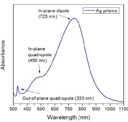
Silver nanoprisms are synthesized using an established protocol (see the Specific procedures section for details) [13]. The UV-vis spectrum of the obtained blue nanoprisms suspension features a sharp peak at 333 nm, a shoulder at around 450 nm and an intense band at around 725 nm (Figure 2.1). These three features are, according to theoretical calculations, assigned respectively to the plasmon resonance of out-of-plane quadrupoles, in-plane quadrupoles and in-plane dipoles. The absence of a peak around 400 nm demonstrates the absence of silver nanospheres.
48
Figure 2.1 UV-vis spectrum of the aqueous suspension of silver nanoprisms.
Successful nanoprisms synthesis is confirmed also by high-resolution transmission electron microscopy (HRTEM) which shows planar particles with triangular shape, mean edge length 34 nm and mean thickness 4 nm. Lattice fringes of ca. 214 pm, corresponding to the (111) orientation, are visible revealing that the nanoprisms are crystalline (Figure 2.2).
49
Figure 2.2 HRTEM images of silver triangular nanoprisms. Side stacking is due to their low
affinity for the support.
The crystalline nature of silver nanoprisms is definitely proved by the X-ray diffraction patterned obtained for a concentrated film of nanoprisms embedded in a poly(vinyl alcohol) (PVA) matrix (Figure 2.3). The presence of only (111) Ag signal is coherent with the currently accepted mechanism of formation of silver nanoprisms, that is selective growth of (111) facets [14].
50
Figure 2.3 XRD pattern of silver nanoprisms showing the (111) peak.
Self-assembly and photocatalytic shaping of silver nanoprisms
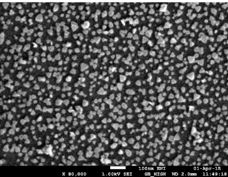
Functionalization of titania with APTES is, as previously mentioned, a necessary step to promote self-assembly of silver nanoprisms (see the Specific procedures paragraph for the necessary details). According to SEM images (Figure 2.4), the titania surface is homogeneously covered with silver nanoprisms.
51
Figure 2.4 SEM image of silver nanoprisms self-assembled on APTES-functionalized
titania.
By direct irradiation in air with 365 nm-UV light of a sample, like that shown in Figure 2.4, silver nanoprisms are changed into spherical nanoparticles. A kinetic study, performed by imaging samples irradiated for increasing times, shows that the photoshaping process is quite fast and that it apparently reaches a plateau after 1 h (Figure 2.5). Rounding of corners and even the disappearance of smaller nanoprisms is visible just after 15 min of irradiation. It has been reported for silver nanoparticles that plasmon-induced charge separation (PICS)-based oxidative dissolution of Ag proceeds preferentially at the sites where the plasmonic near field is strongly localized i.e., for silver nanoprisms, the tips (which are also responsible for the enhanced SERS effect, see below).
52
Figure 2.5 Kinetic investigation of the photocatalytic conversion of silver nanoprisms
into nanospheres.
Transparent titania-coated glass slides are used as substrates to perform the nanoprism irradiation experiments in order to acquire their UV-vis absorbance spectra (Figure 2.6). The observed variations in the position and intensity of peaks support the conclusion that titania-supported nanoprisms are changed into spherical nanoparticles upon irradiation with UV light.
53
Figure 2.6 UV-vis absorption spectra for samples obtained on transparent glass substrates.
Titania films are functionalized with APTES and silver nanoprism suspension is spread only on one face of the substrate. It is apparent that the peak at 850 nm is due to surface-attached silver nanoprisms while the increase in the peak at 450 nm after 1 h of UV irradiation could be ascribed to the presence of smaller, rounded nanoparticles.
Development of patterned SERS scaffolds
The described process opens up new possibilities for the development of patterned SERS-active platforms which would be useful e.g. for sensing applications. As a proof-of-concept, we applied the same lithographic approach described in Chapter 1, exposing a nanoprism-decorated titania film to UV light through a photomask for 1 h to obtain the pattern shown in Figure 2.6 and Figure 2.7a,b.
54
Figure 2.6 Optical microscopy image of the grid replica. The lighter zones are those that
were covered with the photomask.
Figure 2.7 a) Optical and b) electron microscopy magnified images of the resulting pattern.
55
The SERS activity of the obtained patterns is then evaluated. As shown in Figure 2.8a, the SERS peak at 150 cm-1 corresponds to titania [3-5]. This peak in the nanoprism-decorated zones is 20% more intense compared to the UV exposed, nanosphere-decorated zones suggesting that nanoprisms are better SERS enhancers. This makes it possible to obtain a spatially-resolved SERS imaging of the surface, from which the pattern of prisms clearly emerges (Figure 2.8b).
Figure 2.8 a) Intensity of the SERS signal for titanium dioxide in presence of silver
nanoprisms and nanospheres. b) Optical and spatially-resolved SERS image of a patterned sample.
Since the silver nanoprisms are quite near to each other the density of “hot-spots” i.e. of local electric field concentration (due to plasmon resonance) is probably very high, thus leading to the observed enhancement of the SERS signal [15]. The nanospheres not only lack sharp tips, they are also more distant to each other, thus reducing the density of hot-spots.
Preliminary investigations of the shaping mechanism
In order to understand the mechanism for the observed shaping of silver nanoprisms, irradiation experiments are conducted also in the remote photocatalysis mode: silver
56
nanoprisms assembled on APTES-functionalized silicon wafer are irradiated through a titania-coated glass slide for increasing times. However, no appreciable change in the shape and surface density of particles could be detected even after 4 h of irradiation (Figure 2.9). That points out that silver nanoprisms must be in contact with the irradiated titanium dioxide for the shaping process to occur. Another proof for such hypothesis is obtained by performing irradiation of the samples under ethanol. Ethanol is considered to be an efficient hole scavenger [16]. When irradiation is performed under ethanol, the shaping process is considerably slowed down: after 1 h of UV light exposure, bigger prisms retain their shape as observed for irradiation experiments performed in air for 15 min.
These results confirm the photocatalytic nature of the process and indicate that a direct transfer of holes to nanoprisms could be the primary event leading to their shaping into nanospheres.
2.3 Conclusion
Triangular silver nanoprisms can be shaped into spherical nanoparticles using direct photocatalysis. Silver nanoprisms self-assembled on titanium dioxide films are changed into nanospheres upon irradiation with 365 nm-UV light. According to preliminary mechanistic study, this phenomenon is based on the etching of metallic silver through direct transfer of photogenerated holes from the titania to the nanoprisms. Patterned structures can be obtained using simple contact photomasks and their suitability as scaffolds for spatially-resolved SERS is demonstrated.