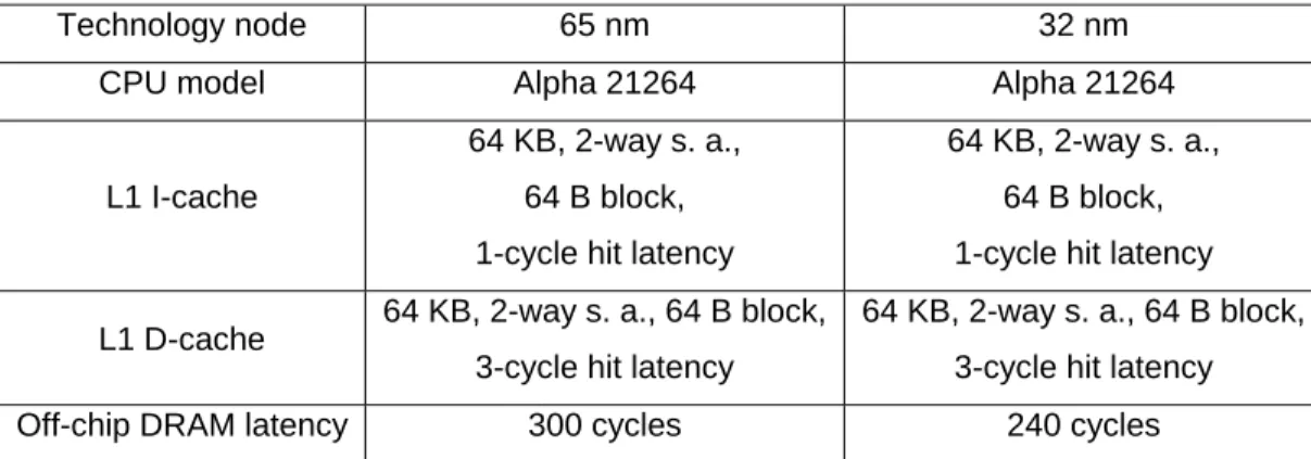
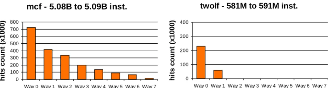
i
SOMMARIO
Tra i problemi principali delle cache di ultimo livello impiegate negli odierni microprocessori vi sono il wire delay e il consumo di energia statica. Le cache NUCA (Non Uniform Cache Architecture) limitano l’impatto del wire delay grazie al partizionamento in un insieme di banchi di memoria di ridotte dimensioni e tempo di accesso, accedibili indipendentemente l’uno dall’altro per mezzo di una Network On Chip. In particolare, le cache D-NUCA adottano un meccanismo di migrazione dei dati più frequentemente acceduti verso i banchi più vicini al controller centrale. Grazie alla loro modularità e al meccanismo di migrazione dei dati è possibile applicare alle cache D-NUCA una tecnica microarchitetturale di riduzione del consumo di energia statica a basso costo implementativo (Way Adaptable D-NUCA). Tale tecnica è basata sull’attivazione/disattivazione dinamica di gruppi di sottobanchi: nel corso dell’applicazione, le porzioni di cache sottoutilizzate possono venire disattivate, riconfigurando dinamicamente il numero di vie della cache in base ai requisiti dell’applicazione.
In questa tesi viene valutata l’efficacia della tecnica in un contesto CMP, in cui due core condividono la stessa cache D-NUCA di ultimo livello. Differenti metodologie di ottimizzazione della tecnica sono poi esplorate e valutate, e, in alternativa all’ottimizzazione dei parametri della tecnica per ogni applicazione, viene proposta una famiglia di algoritmi non basata su parametri numerici.
Viene poi effettuato un confronto, in termini di prestazioni e risparmio energetico ottenibile, tra la tecnica Way Adaptable D-NUCA e altre tecniche power saving proposte in letteratura, applicate alle D-NUCA, quali Decay Lines Cache e Drowsy Cache, proposte per cache convenzionali, che agiscono con granularità più fine, a livello di linea, e non di via. Tale confronto viene effettuato per stabilire come si posiziona la tecnica Way Adaptable D-NUCA rispetto a queste, in termini di tradeoff tra costo implementativo e risparmio energetico ottenibile.
Viene infine proposto e valutato uno schema innovativo di risparmio energetico che combina Way Adaptable D-NUCA e Drowsy Cache, in grado di limitare gli effetti che ha la variazione statistica di processo sulle tecniche di riduzione del consumo di energia statica per gli odierni processi produttivi.
ii
ABSTRACT
Large last level caches are a common design choice for today’s high performance microprocessors, but ever shrinking feature size and high clock frequencies exacerbate the wire delay problem: wires don’t scale as transistors do, and their latency is going to be the main component of cache access time. Further, leakage power is becoming the main power issue for large last level caches in deep sub-micron processes.
NUCA (Non Uniform Cache Architecture) caches limit the impact of wire delays on performances by aggressively partitioning the cache into independently accessible small and fast sub-banks, interconnected by a scalable network-on-chip. D-NUCA caches, in particular, implement a migration mechanism on frequently accessed data by dynamically moving them into the banks closer to the controller, hence accessed faster.
By leveraging their modularity and the non uniform distribution of data it is possible to apply to D-NUCA caches a microarchitectural leakage reduction technique, the Way-Adaptable D-NUCA, which applies power gating to groups of underutilized banks, dynamically resizing the cache in the course of the application.
This thesis evaluates the effectiveness of this technique in a multiprocessor environment and explores different optimizations to enhance its efficiency; in particular, alternative resizing algorithms are investigated.
The Way Adaptable technique is then compared to other leakage reduction techniques proposed in literature, Decay Lines Cache and Drowsy Cache, in order to determine the additional leakage savings when circuital fine-grained leakage reduction schemes at line level are applied to D-NUCA caches.
Finally, a leakage reduction scheme combining Way Adaptable and Drowsy Cache, in order to cope with leakage reduction limits posed by statistical process variation effects of nanometer processes, is proposed and evaluated.
iii
RINGRAZIAMENTI
Questa tesi riassume le mie attività di ricerca portate avanti durante il triennio di dottorato. Un sentito ringraziamento va al Prof. Cosimo Antonio Prete, che mi ha permesso di entrare a far parte del suo gruppo di ricerca e al Dr. Ing. Pierfrancesco Foglia, che ha supervisionato le mie ricerche in prima persona rappresentando per me un valido riferimento.
Profonda gratitudine e stima va poi ai miei colleghi di corso e compagni di ricerca, con i quali attivamente ho collaborato e tuttora collaboro: Alessandro Bardine, Stefano Campanelli, Giacomo Gabrielli, Francesco Panicucci e Marco Solinas, per gli stimoli, gli spunti di discussione ed il sostegno amichevole.
Un pensiero di affetto va poi a tutti coloro che nel tempo sono stati miei compagni di ufficio, tutti i ragazzi di TRIO, di UniPos e del PerLab, nonché i miei colleghi di corso.
La mia attività di ricerca è stata svolta nell'ambito di due iniziative internazionali: il network di eccellenza europeo HiPEAC ed il progetto di ricerca integrato SARC, entrambi parte del 6° programma quadro della comunità europea.
iv
ACKNOWLEDGEMENTS
This thesis summarizes my research activity during this PhD triennium. I wish to sincerely thank Prof. Cosimo Antonio Prete, who welcomed me in his research group and Dr. Ing. Pierfrancesco Foglia, who personally tutored me being my mentor and my point of reference for all this time.
My gratitude goes then to my research fellows, with whom I've actively worked: Alessandro Bardine, Stefano Campanelli, Giacomo Gabrielli, Francesco Panicucci and Marco Solinas, for all the sprones, suggestions and the friendly support. My thought goes to all my current and past officemates, all TRIO, UniPos and PerlLab guys, and all my PhD collegues.
Finally I wish to remember that all my work has been performed in the context of two international European initiatives: the European HiPEAC network of excellence and the SARC research project, both financed by the European Commission under the 6° framework program.
v
CONTENTS
SOMMARIO... I
ABSTRACT ... II
RINGRAZIAMENTI... III
ACKNOWLEDGEMENTS ...IV
CONTENTS ...V
1 INTRODUCTION ... 1
1.1 ISSUES IN ON CHIP LARGE CACHE MEMORIES ... 1
1.1.1 Wire delay... 1
1.1.2 Leakage power consumption ... 2
1.2 NUCA CACHES ... 5
1.2.1 S-NUCA Architectures ... 8
1.2.2 D-NUCA Architectures ... 9
2 RELATED WORK... 12
2.1 Novel high performance and power efficient cache architectures... 12
2.1.1 NUCA architectures: Rationale and first proposal... 14
2.1.2 Other NUCA design alternatives ... 19
2.1.3 Reconfigurable cache architectures ... 29
2.2 Line-level leakage reduction techniques in conventional caches ... 36
2.2.1 State destroying techniques... 36
2.2.2 State preserving techniques... 40
vi
3.1 Modelling system performances ... 45
3.2 Modelling D-NUCA caches, assumptions ... 48
3.3 Modelling power consumption... 49
4 WAY ADAPTABLE D-NUCA CACHE... 51
4.1 A leakage reduction technique for D-NUCA Caches... 51
4.1.1 Rationale ... 51
4.1.2 Way Adaptable D-NUCA ... 55
4.2 Way Adaptable D-NUCA: tuning methodologies and optimal parameters... 59
4.2.1 Way Adaptable D-NUCA: Poll rate exploration ... 59
4.2.2 Way Adaptable D-NUCA: Threshold exploration... 61
4.3 Way Adaptable D-NUCA in the CMP environment... 67
4.3.1 Reference Architecture ... 67
4.3.2 Simulation methodology and performance metrics ... 67
4.3.3 Results ... 70
4.4 Evaluation of workload-independent strategies for Way Adaptable D-NUCA Caches... 73
4.4.1 Motivation... 73
4.4.2 Rationale ... 74
4.4.3 Results ... 77
4.4.4 Discussion... 79
4.4.5 Coping with oscillatory behaviours ... 80
5 A COMPARISON OF LEAKAGE REDUCTION
METHODOLOGIES FOR D-NUCA CACHES ... 87
5.1 D-NUCA Drowsy Caches ... 87
5.1.1 Introduction... 87
5.1.2 Drowsy parameters explored ... 88
5.1.3 Results of exploration ... 90
5.2 Decay Lines D-NUCA... 94
vii
5.2.2 Decay D-NUCA Caches exploration ... 95
5.2.3 Results ... 95
5.3 Comparison of the three techniques... 100
5.4 Coping with process variation ... 104
5.5 Combining Drowsy Cache with Way Adaptable... 105
5.5.1 Rationale ... 105
5.5.2 Results ... 106
6 CONCLUSIONS ... 111
APPENDIX A: COMPUTATIONAL COMPLEXITY OF THE
PROCEDURE TO DETERMINE THE OPTIMAL SEQUENCE OF
RECONFIGURATIONS ... 113
1
1 INTRODUCTION
1.1 ISSUES IN ON CHIP LARGE CACHE MEMORIES
1.1.1 Wire delay
Microprocessor design today is characterized by two main features, among others: big capacity last level caches[8][9][10] and cores replication (CMP) [10][11]. Both of these aspects are a natural way of leveraging the ever growing number of transistors available on the die, with a limited design and verification effort. In fact, continuous manufacturing advances in semiconductor technologies are still satisfying nowadays the famous Moore’s predictions [1]. The feature size shrinking of manufacturing processes (chips implemented in 32 nm technology are currently marketed today and Intel is planning to start the production of 22 nm chips by the end of 2011) together with growing integration capabilities, reduces transistor switching time, enabling for higher clock frequencies for microprocessor pipeline that translate in performance improvements. On the other hand, the performances of on-chip conventional caches are jeopardized by the wire delay problem [2][3][5]. The sizes of metal wires on the die have been shrunk accordingly to transistor feature size, causing an increase in the wire resistance per unit length, due to smaller cross sectional areas. However the capacitance characteristics of such interconnect has not reduced proportionally, causing wires to scale worse with respect to transistors. Being the latency associated to interconnect related to the product between wire resistance and wire capacitance, modern manufacturing processes see relatively slower wires with respect to transistors. This factor, together with higher clock speeds, limits the number of transistors reachable by electrical signals on chip in a clock period [4][3]. Figure 1 shows the portion of a fixed-area die reachable in a single clock cycle on a global (repeated) wire when process feature size is projected from 180 nm to 35 nm. The effect of wire delay is detrimental both for memory-based monolithic structures in the pipeline [2] (such as large register files and reorder buffers) and, of course, caches.
2 For what concerns large monolithic SRAM caches, such as last level caches employed in modern microprocessors, made up of millions of transistors, the main access latency contribution is the latency of signal routing to and from banks and not the banks access latency itself. According to a traditional organization of these memories ([6]), this latency will be lower limited by the time to reach data that physically reside in the farthest regions of the memory with respect to the cache controller.
In [7] the nominal unloaded access latency of a traditional L2 cache for technologies from 130 nm to 50 nm is projected to grow from 13 to 41 clock cycles (for a 2MB and a 16MB cache respectively). For the same cache architectures, the loaded cache access latency (evaluated using real workloads and taking into account cache contention) steps from 68 to 255 clock cycles, for the 130 nm 2MB cache and the 50 nm 16MB cache respectively. This indicates that wire delay is going to play a significant role in the design of large last level caches in deep submicron technologies and wire delay tolerant designs for caches are highly desirable.
1.1.2 Leakage power consumption
The large die area fraction occupied and the scaling trends of deep submicron CMOS technologies greatly enforce the role of static power component caused by
Figure 1 picture from [5], cap 3 section 2. Distance in a clock cycle on a 17.6 mm side die under technology scaling .
3 leakage currents for on chip last level caches. Leakage energy is consumed by all transistors in the die regardless of their switching activity (which, in turn, causes dynamic energy consumption) as long as they are connected to power supply. Leakage is a power component of CMOS circuits together with switched capacitance and short circuit currents[13] (which are dynamic components). Switched capacitance is the main component of dynamic power consumption and originates by charging and discharging of output capacitances, while short circuit currents cause power consumption in the short fraction of time during switching in which both the NMOS and PMOS transistors of a unit are on. The main parameters of switched capacitance power are supply voltage V, clock frequency f, physical capacitance C and switching activity factor α. This main dynamic power component is related to these parameters by the well known formula Pdyn≈αCV2f, which
expresses the different alternatives for reducing dynamic power consumption: transistor and wire sizing for reducing C, switch activity reduction (i.e. by clock gating), frequency and voltage scaling. This last two options, often combined (DVS, dynamic voltage scaling [15]) are the most adopted techniques ([16][17][18]). On the other hand, idle, or leakage power is rapidly becoming the main source of energy consumption for circuits[14], due to electrical characteristics of deep submicron transistors and high component integration. Leakage current is, in turn, composed of various components, of which the main are subthreshold leakage and gate-oxide leakage. Subthreshold leakage current of a transistor flows between its drain and source and can be modelled by equation (1),
⎟⎟
⎠
⎞
⎜⎜
⎝
⎛
−
=
− − T V nT V subKWe
e
I
th1
(1)where W is the gate width, K and n are electrical constants, Vth is the transistor
threshold voltage and T is the temperature. Among the other parameters, leakage current depends on temperature and threshold voltage. As technology scales, threshold voltage has to be scaled along with supply voltage potentially causing an increase in subthreshold leakage. Gate-oxide leakage current flows from the gate of the transistor to the substrate and depends on the thickness Tox of the oxide
4 V T ox ox ox
e
T
V
W
K
I
⎟⎟
−α⎠
⎞
⎜⎜
⎝
⎛
=
2 2 (2)The deeper the shrinking becomes, the higher this component is going to be, since gate oxide’s thickness has to scale together with transistor length and supply voltage. The latter component of leakage current is becoming a growing problem for current manufacturing processes (45 nm and beyond) and can be addressed using high-k insulators for gate [19].
Leakage currents can be reduced using purely electrical techniques, such as novel manufacturing techniques (such as high-k dielectrics for gate leakage), or raising threshold voltage of transistors. An efficient, yet costly, method of reducing leakage is cooling the circuit, since leakage depends on temperature. Leakage can be addressed by dynamically reducing operational voltage V or by gating the leaking circuit from supply, if possible. These last two techniques are often combined with microarchitectural techniques which are discussed in the remainder of this thesis. The more transistors a component of the processor is made of, the higher leakage energy consumption it is going to suffer, regardless of its average switching activity. In this perspective, leakage power consumption can be roughly correlated to the fraction of die area a given component occupies.
Figure 2 shows the die of the 45 nm quad core i7 Intel processor: a large fraction of the die area (a total of 731 Million transistors is integrated on 263 mm2 area) is occupied by the large 8MB L3 cache, and each of the four cores hosts 256 KB of L2 cache. As expected, large SRAM structures currently employed as last level caches of today’s microprocessor designs, account for a large portion of the total leakage energy consumption of the processor, and, in turn, must be one of the main targets for overall chip power efficiency[20].
5
1.2 NUCA
CACHES
This section exposes the rationale and main concepts of NUCA (Non Uniform Cache Architecture) according to the first work which defined it [7]. A lot of research effort has followed this original proposal, covering performance and energy related issues as well as chip multi processor performance. A presentation of this additional related work will be given in 2.
NUCA [7][21] is an architectural proposal for large on chip caches whose first purpose is to overcome the issue of wire delay induced by technology scaling. By definition, each cache memory in which access latency is not uniform but depends on the physical position of the requested datum is NUCA, nevertheless all “explicitly NUCA” architectures have in common aggressive sub-banking and an adequate interconnection infrastructure which is able to guarantee independent access to each sub bank. The idea of NUCA is to replace a large and monolithic (i.e. with constant and potentially high latency) traditional cache with a matrix of small (for this reason potentially faster) sub-banks, connected with the controller by means of a communication fabric, such as a Network on Chip (NoC) in order to guarantee independent access to each sub-bank.
Figure 2 45nm Intel Core i7 die photography. The area occupied by the last level 8 MB cache is shown on the bottom of the picture. The total die area is 263 mm2.
6
Figure 3 Reference 16x8 NUCA architecture evaluate in this thesis. A total 8MB memory capacity is given by the sum of 128 64KB small cache banks, connected to the central controller by means of a switched network on chip.
The black circles in the picture depict network switches.
Figure 3 shows a system equipped with the reference NUCA L2 cache that will be used in this thesis. This cache has an overall capacity of 8 MB, given by the sum of the single capacities of 128 independent 64KB small banks. The banks are connected among them and with the controller through a partial 2-D mesh network, in which all horizontal links are present but only a column of banks is equipped with vertical links. Each sub bank is a self contained cache memory and can be accessed independently from the others. The Network on Chip is made of network switches (in this architecture, one switch is placed at each bank) and bidirectional links, which are able to deliver messages from the controller to the banks and back. The network is assumed to be packetized, and requests are broken into flits (the unit of traffic sent on the network). Packets are made up of commands (read/write commands for the sub banks) and, potentially, data (read replies from the banks to the controller and write payloads from the controller to the banks). In a wire delay dominated environment, the main contribution to access latency is given by the signal transmission latency over wires which connect banks and sub banks to the controller. A traditionally organized monolithic cache, also indicated in the following
7 as UCA (Uniform Cache Access) is often sub-banked as well, but it can only be accessed at the speed of the farthest sub bank (from the controller) which is also the slowest[6]. A NUCA, instead, has a different latency for each bank, depending on its physical distance (in a mesh environment, it can be assumed as the Manhattan distance). Because of the different interconnect with respect to a traditional cache (in [6] hierarchical H trees are employed), banks closer to the controller can be accessed faster and independently from the other ones (each cache line will be stored in a single cache sub bank). If, in particular, the cache line requested by the controller belongs to the first bank column (Figure 3), only a small portion of the network must be traversed; on the other hand, if the requested bank is located farther away, a longer trip on the network is required. Since for both cases access latencies are dominated by signal propagation on the network and sub-banks are small and fast, in the former case the access latency will be reduced with respect to the latter.
The particular modular design gives a lot of room for different design solutions, for instance regarding to data allocation and mapping to banks and search policies. The mapping rule determines how each cache line is mapped to banks. Two families of mapping can be identified: static and dynamic.
Static mapping states that each cache line can be mapped exclusively to a single bank, univocally determined by a portion of its memory address. NUCA caches based on static mapping are called S-NUCA (Static NUCA).
Dynamic mapping, instead, links each cache line to a set of different sub-banks (a bankset). A cache line can be found in each of the sub-banks of its bankset, since it’s expected to migrate dynamically, at run time, from one bank to the other of the bank set (to improve performance). Dynamic mapping improves performance but complicates design, since it introduces the need of a search policy to find the current bank which contains the cache line inside the bankset. The particular bankset in which the search has to be performed is determined statically from the cache line address. NUCA caches adopting the dynamic mapping (hence data migration) are called D-NUCA (Dynamic NUCA). It is important to note that the rest of the memory hierarchy is agnostic with respect to the NUCA cache architecture,
8 since no difference can be noticed from outside the main cache controller, and the NUCA cache functionally behaves as a traditional one.
1.2.1 S-NUCA Architectures
In an S-NUCA each cache line can be found only in a single bank, statically based on its memory address. In this case there’s no need for the cache search mechanism to involve more banks. Upon a cache line access request (e.g. a read request) the controller determines the bank which could contain the datum from the memory address and injects a request into the network addressed to the target bank (a basic bank naming strategy is assumed to properly route packets throughout the network). In case of a cache read hit, a reply packet will be locally prepared and sent back to the controller, containing the data block. In case of a cache miss a control packet can be sent back to the controller to acknowledge the end of the cache access and propagate the miss to the lower levels of memory for its resolution. In this kind of architecture, set associativity can be realized by making each bank set associative, and the overall degree of associativity of the cache will be given by the associativity of each sub-bank. A similar procedure, mutatis mutandis, holds for write requests (or cache fills). Despite the simple design and management policies, an S-NUCA cache exhibits lower average access latencies with respect to traditional UCA caches (Uniform cache architecture), basically because there is no need to wait for the signal to propagate up to each bank. However, as the data mapping is solely based on the memory addresses and it doesn’t take into account the different usage frequencies of data, it may end in a suboptimal placement of data into banks, leading in higher access latencies with respect to smarter designs. It is worth noting that data locality is inherently dynamic and varying across applications and different phases of the same application, hence no static allocation may be satisfying in order to adequately leverage non uniform cache access latency.
9
1.2.2 D-NUCA Architectures
In a D-NUCA cache a portion of the address determines statically the particular bank set in which a cache line can be find. At runtime, the cache line will be moved across its pertaining bank set, following an intra-set dynamic bank assignment strategy aimed at lowering cache access time of frequently accessed data.
For example, in the reference D-NUCA of Figure 3, the banks are logically grouped in rows and columns, and a bank set is made up of all banks belonging to the same row. So a cache line can be hosted by all the banks belonging to a given row based on its memory address. When a cache line search is performed, the controller injects a request packet in the network addressed to all the banks of the pertaining horizontal bank set (meaning that only the vertical component is specified). This request will be multicast to all the banks of the row that can contain the data. Figure 4 shows the search operation in the reference D-NUCA: the
Figure 4 Multicast search policy. On the left side of the picture the miss case is represented, on the left a hit in the sixth column(way) happens. Red arrows
10 request first traverses the vertical links to reach the pertaining bank set, then traverses the horizontal links and switches and, at each switch, is replicated to the local bank. The particular network topology and switch assignment permit to implement multicast across a bank set with reduced cost. It is worth noting that the network topology depicted in Figure 3 is a partial mesh, where only a row of vertical links is present. Upon packet receiving, a search is performed inside each sub bank. In case of an overall cache miss each cache search will result in a miss reply packet, and n misses (M in the figure) will happen, with n being the depth of the bank set; in case of a hit, one bank in the bank set will incur in a hit (H in the figure). The bank containing the datum sends a reply to the controller that follows the inverse path of the request message. It is worth noting that as soon as the hit happens, the request is satisfied without the need of waiting for the replies from the other, farther, banks. As a line can stay only in one bank of the set, the cache globally behaves like an n-way set associative cache, the ways being the columns of banks. It is worth noting that the dynamic data mapping implements associativity in a different way with respect to S-NUCA: in a D-NUCA cache, each of the n banks of the bank-set can (and, actually, in this reference architecture, is) be direct mapped.
The reduced access latency with respect to an S-NUCA comes from the data migration mechanism adopted in a D-NUCA cache. Internally to each bank set, most frequently accessed data are migrated towards the sub banks closer to the processor. This migration can be implemented with a “promotion/demotion” mechanism: as soon as a hit happens in a bank which is not pertaining to the first row (the row closer to the cache controller) the cache line is “promoted” by copying it in the cache block that holds the same position in the next bank closer to the controller. The corresponding cache line in the arrival bank is copied back to the former bank, implementing a sort of “swapping”, which speculatively assumes that the last accessed cache line (which has been migrated forward) will be accessed again soon. As a consequence, if sufficient data locality is exhibited by the application, the most frequently accessed lines are likely to be located into the banks closer to the processor, reducing overall cache access latency. If a miss happens, the line is retrieved from the main memory and is inserted in the farthest
11 bank (i.e. the one in the last column) of the pertaining set, possibly evicting any corresponding line. With such a policy, D-NUCA caches succeed in achieving high hit rates while keeping the access latency low, in spite of the wire-delay effects introduced by high clock rates and technology scaling. This makes the D-NUCA rationale and paradigm attractive for cache designs of next generation high performance chips, where large storage capabilities, high clock rates and low memory access latencies will be required. The behavior of D-NUCA exposed so far, chosen as a reference for this study, is one set of possible choices regarding different search and miss handling mechanisms, which will be exposed in 2.
12
2 RELATED
WORK
2.1 Novel high performance and power efficient cache
architectures
The first proposal of NUCA and the D-NUCA cache architectures [7][21] showed that a Dynamic NUCA architecture was able to limit the impact of wire delays on performances achieving an IPC 1.5 times higher than a traditional Uniform Cache Architecture (UCA), for single core applications, when maintaining the same size and manufacturing technology. Extensions to this original idea are NuRapid[22], Triangular D-NUCA cache [23] and clustered D-NUCA schemes[27]. They improve performance by decoupling tags from data or by changing mapping and size of each way. The authors of [22] employ a tag array physically decoupled from the main data array structure, implementing a more flexible data mapping and improving dynamic energy efficiency, reducing the number of bank accesses upon each search. Triangular D-NUCA cache [23] is an architectural proposal in which the mapping and sizes of each way are not kept constant, showing as a judicious mapping policy can result in an energy efficient architecture. In [27] an accurate NUCA latency modelling is adopted and a clustered scheme is proposed in order to limit network latency when relatively high traversal latency of synchronous switches poses limits on performance. In the context of on-chip multiprocessors, the behaviour of D-NUCA as shared L2 caches has been analyzed in [24][25][26][47], evaluating the performance of different data mapping schemes and migration policies, but none of these works explicitly focuses on power and energy aspects. ESP-NUCA[28] (Enhanced Shared-Private NUCA) combines benefits of private and shared caching for CMPs, employing different mapping policies for shared and private data. In [46] a novel data remapping strategy for S-NUCA is evaluated, for multithreaded workloads.
In the context of traditional cache architectures (not NUCA) a lot of work has been proposed to dynamically adapt the cache size to the working set size. Most of these techniques are focused on performances and dynamic power savings and are not directly applicable for reducing the static power consumptions. In particular,
13 Selective Cache Ways[29], Accounting Cache[30] and Configurable Cache[31] have been proposed. All these techniques require an always powered on cache to reduce miss rate and dynamic power consumption.
The microarchitectural techniques focusing on the reduction of static power consumption[13] rely on putting portions of the cache (usually, with cache line granularity) in a low leakage mode. This operation can be state preserving (i.e. the low leakage mode allows for the datum stored in the cache to be maintained) or state destroying (meaning that once a cache line is put in low leakage mode its potentially valid stored content is lost). MTCMOS Caches[32] and Drowsy Caches[33] are state preserving techniques while Decay Lines Caches[34] is a microarchitectural state destroying technique employing Gated VDD[35] to reduce
leakage consumption of cache lines. In this thesis, their performance and energy efficiency will be evaluated in the context of a D-NUCA cache.
The Way Adaptable Cache[36] is a state destroying technique that predicts cache needs adopting a metric based on the LRU/MRU state of each way and turns on and off entire ways based on a random choice. The direct application of this technique to a D-NUCA would imply the complexity of calculating the LRU/MRU state; furthermore, the random choice of a way to turn off wouldn’t take into account the actual usefulness of data.
None of the aforementioned work explicitly combines a NUCA cache with a leakage reduction policy suitable for a non uniform architecture. In [45] an energy model for S-NUCA and D-NUCA caches is proposed, and power efficiency of NUCA architectures is shown to be superior to UCA. This energy model is adopted in this thesis, adapted to a projected 32nm manufacturing process and extended to model reduced leakage states such as drowsy state[33]. Recently, a leakage reduction technique targeted for D-NUCA caches, the Way Adaptable D-NUCA cache[39][40] has been proposed. The idea proposed in [39][40] is further studied and developed in this thesis, its applicability to a CMP environment[37][41] is evaluated and a comparison with state of the art leakage reduction technique is performed, together with the proposal of a novel hybrid Way Adaptable Drowsy D-NUCA cache in order to tolerate process variation effects. In the context of dynamic energy consumption reduction, in [38] a controlled migration mechanism
14 is proposed to reduce the number of bank accesses on concurrent subsequent hits on conflicting cache lines into two adjacent banks.
Finally, this work is related to the more general context of detecting program phases[42] to adapt the number of active resources to the need of the running program. In [43] a comparison of ideal and actual implementations of such techniques is proposed.
A general overview upon different topics about NUCA caches can be found in [44]. In the following, various NUCA architectures are presented, from the original proposal to other various solutions presented in literature.
2.1.1 NUCA architectures: Rationale and first proposal
In [21][7] the NUCA architecture is defined and the achievable performances of different NUCA solutions is explored, together with some seminal considerations on energy efficiency. This work evaluates different cache configurations (UCA, S-NUCA and D-S-NUCA, Figure 5) for a 16 MB L2 cache memory implemented in a projected 50 nm manufacturing process. In Figure 5(a) all the available 16 MB cache memory is used to implement a traditional L2 UCA cache, while in Figure 5(b) the total available space is partitioned in two levels resulting in an L2-L3 hierarchy (multi level UCA, ML UCA in the following) made up two traditional caches. This second solution results in lower overall latency, but reduced overall capacity: since this cache hierarchy obeys to the inclusion principle, part of the L3 capacity is used to store a copy of data stored in L2. In Figure 5(c) this preliminary sub-banking is extended and semantically modified to implement an aggressively banked S-NUCA cache, with non uniform access latency and no need for data replication (no inclusion is needed, since a datum can exclusively reside in a bank or in another). The interconnection network is a set of per bank private, two-way, pipelined transmission channels. This non uniform architecture is referred as S-NUCA 1 in the following. In Figure 5(d) the private channels are substituted by a two-dimensional switched network allowing a consistent space saving and a further aggressive bank partitioning (S-NUCA-2).
15 The D-NUCA architecture, similar to the one presented in 1.2.2 is depicted in Figure 5(e). The proposed architectures are evaluated through execution driven simulations based on an extended version of the single core sim-alpha simulator[48] running highly L2 intensive phases of applications selected from the SPEC CPU2000, the NAS and the speech benchmarking suites. Assuming a constant L2 cache area and varying the manufacturing technology from 130 nm to 50 nm, the work explores, for the UCA organizations, the resulting size of the cache and its achieved performance. Table 1 summarizes the results of this preliminary evaluation. When moving from 130 nm down to 50 nm, because of technology scaling a cache size increase from 2MB to 16MB is possible. The L2 miss rate decreases with the size of the cache, but both the unloaded and the loaded latency increase as a result of the increasing wire delay effect. This second effect overwhelms the miss rate reduction causing performance degradation, measured as an IPC (Instruction per cycle) loss. This trend does not favour the adoption of large monolithic cache structures as UCA caches for wire delay dominated environments, since cache access latency is not expected to scale efficiently.
A first evaluation of the performance improvements achievable with aggressive sub-banking and independent bank access is given by S-NUCA-1 and summarized in Table 2. Using dedicated, per bank, links incurs in area overhead, limiting the possible degree of sub-banking, hence the bank access latency reduction.
Figure 5 Different cache architectures evaluated in [7]. Numbers indicated in the banks are unloaded access latencies in clock cycles, while average loaded latencies are indicated below the number of banks at the bottom of each picture. Loaded latency takes into account link and bank contention.
16
Table 1 Performance evaluation for different sizes/manufacturing processes of traditional (UCA) architectures.
Tech (nm) L2 Size Num Sub-banks Unloaded Latency Loaded Latency IPC Miss Rate 130 2 MB 16 13 67.7 0.41 0.23 100 4 MB 16 18 91.1 0.39 0.20 70 8 MB 32 26 144.2 0.34 0.17 50 16 MB 32 41 255.1 0.26 0.13
Table 2 Performance evaluation for different sizes/manufacturing processes of SNUCA-1 (Figure 5 c) architectures.
Unloaded Latency Conservative Aggressive Tech
(nm) L2 Size
Num
banks Bank Min Max Avg Load
lat IPC Load lat IPC 130 2 MB 16 3 7 13 10 11.3 0.54 10.0 0.55 100 4 MB 32 3 9 21 15 17.3 0.56 15.3 0.57 70 8 MB 32 5 12 26 19 21.9 0.61 19.3 0.63 50 16MB 32 8 17 41 29 34.2 0.59 30.2 0.62
Table 3 Performance evaluation for different sizes/manufacturing processes of S-NUCA 2 (Figure 5 d) architectures.
Unloaded Latency Tech (nm) L2 Size Num
banks Bank Min Max Avg Load lat IPC 130 2 MB 16 3 4 11 8 9.7 0.55 100 4 MB 32 3 4 15 10 11.9 0.58 70 8 MB 32 5 6 29 18 20.6 0.62 50 16MB 32 8 9 32 21 24.2 0.65
Table 4 Performance evaluation for different sizes/manufacturing processes of baseline D-NUCA (Figure 5 e) architectures.
Unloaded Latency Tech (nm) L2 Size Num
banks Bank Min Max Avg Load lat IPC 130 2 MB 16 3 4 11 8 9.7 0.55 100 4 MB 32 3 4 15 10 11.9 0.58 70 8 MB 32 5 6 29 18 20.6 0.62 50 16MB 32 8 9 32 21 24.2 0.65
The unloaded latencies are calculated for the single bank (not accounting for wire delay time), for the banks closer to the processor (min column in Table 2), for the farther ones (max column in Table 2) and as average. The loaded latencies are evaluated assuming two alternatives for solving a contention: a conservative policy that assumes that each request on a channel can start only when the previous one
17
Figure 6 The three different mapping policies for D-NUCA bank sets proposed in [7].
has completed and an aggressive one assuming channel pipelining and the ability of starting a new request every d cycles, where d is the single bank latency. Unlike the UCA case, the average IPC increases as the cache sizes increases until 8MB, while for the 16 MB case the relative average hit latency degradation is not compensated by miss rate reduction. In S-NUCA-2 a more area efficient interconnection network is evaluated (2-D, full mesh connected switched network). The mesh consumes less area than the private, per bank channels, resulting in smaller area occupancy and reducing overall wire latencies. Faster access time to all banks is provided, leading to a scalable solution and to a 10% IPC increase for the 16 MB cache Table 3.
A wide section of [7] is then devoted to describing the D-NUCA solution, discussing the design space of this kind of architecture. Basically, the different choices that can be done for a D-NUCA architecture concern: data mapping; search strategy; data movement and replacement.
The data mapping strategy (Figure 6) determines the association of banks to banksets, hence the implementation of set associativity. Three different mapping policies are presented: simple mapping, fair mapping and shared mapping. Simple mapping maps each column of banks to a set, and each row of Figure 6 behaves like a way of a set associative cache.
To avoid different bankset access latencies given by different horizontal delays, fair mapping is proposed: in order to guarantee equal access time to each set bank from different columns are allocated to each bank set. Finally, shared mapping allows for sharing the same sub bank between two bank sets, in order to provide faster access to all the sets.
18 Search strategies relate to the policies used to search a cache line inside a bank set. Incremental search completes the search to each bank (from the closer to the farther) before searching in the following, while multicast search uses a replication mechanism at each switch in order to trigger more searches in parallel: at each bank the search is initiated as soon as the request packet can be decoded by the local bank, without waiting for the previous banks to complete and notify the controller. Multicast search offers higher performance but increases energy consumption.
Data movement is implemented by means of a generational promotion policy: when one (or more) hits occur to a cache line, the datum is swapped with the corresponding one located in the next bank closer to the controller, if any. The length of this mutual hop, in terms of banks, as well as the number of hits to trigger a swap are parameters of the policy. Various line insertion policies upon miss resolution are evaluated: “tail insertion” in which new data are inserted in the farthest banks, “head insertion” in which the new line is inserted in the closest bank and “middle insertion” in which the new line in inserted in the middle banks. The replacement policies evaluated are: “zero-copy”, in which the victim line of the insertion is evicted from the cache, and “one-copy”, in which the victim is moved to a lower-priority bank replacing a less important line farther from the controller. Table 4 shows the performance of the baseline D-NUCA configuration which uses the simple mapping, multicast search, tail insertion and for each hit promotes the line of a single bank towards the controller. The experimental results show that D-NUCA outperforms S-D-NUCA-2 in terms of IPC ranging from 4% to 10%. This baseline set of D-NUCA policies is the one taken as reference in the remainde of this thesis.
Table 5 compares the achievable performance improvements of the various proposed policies for line search, mapping, promotion and eviction.
19
Table 5 Exploration of different search, promotion, eviction and mapping policies for D-NUCA compared to baseline.
Policy Avg lat IPC Miss rate Bank Access Search policies Incremental 24.9 0.65 0.114 89M 2 mcast + 6 inc 23.8 0.65 0.113 96M 2 inc + 6 mcast 20.1 0.70 0.114 127M 2mcast + 6 mcast 19.1 0.71 0.113 134M Promotion Policies 1-bank/2hit 18.5 0.71 0.115 259M 2-bank/2hit 17.7 0.71 0.114 266M 2-banl/2-hit 18.3 0.71 0.115 259M Insertion-Eviction Policies
Ins head, evict rnd 15.5 0.70 0.117 267M Ins middle, evict rnd 16.6 0.70 0.114 267M
Mapping Policies
Shared 16.6 0.73 0.119 266M
Baseline (simple mapping, multicast search, 1 bank/1hit promotion, insert at tail)
18.3 0.71 0.114 266M
2.1.2 Other NUCA design alternatives
2.1.2.1 NuRapid
Chisti et al. in their work [22] describe some limitations of the NUCA cache architecture proposed in [7] (in the following simply referred as NUCA). In this perspective, they propose a “Non-Uniform Access with Replacement And Placement using Distance Associativity” cache architecture (NuRAPID). The main feature of NuRAPID architecture is decoupling tag arrays from data arrays. In this architecture tags are located in a centralized array near to the controller, which is accessed before data array (implementing an efficient sequential tag-data access). Upon a hit in the tag array, a pointer is used to identify which block in the NUCA portion of the cache contains the data.
As shown in Figure 7 the tag array is implemented as a conventional set-associative cache, while “distance associativity” is proposed as a flexible technique to implement set associativity in the data array: the latter is divided in “distance groups” (d-group in the figure). Banks pertaining to the same d-group have the same latency, and each group can host cache lines coming from any set (thanks to the decoupling strategy implemented by the pointers in the tag array).
20 So, if the application requires it, all the ways of a single set can be placed in the faster d-group. In this perspective, the sequential access to tag and data aims to reduce dynamic energy consumption spent in the banks and in the interconnection network due to NUCA multicast search policy, while avoiding performance losses of NUCA sequential search. On the other hand, the concept of “distance associativity” decouples tag and data placement allowing for more efficient placement of frequently used data. Two promotion policies are also proposed: next-fastest and fastest. In next-fastest when a line in a d-group is accessed it is swapped with a line in the next d-group closer to controller. Thanks to the decoupling mechanisms exposed before, the two swapping lines do not need to belong to the same set. The fastest promotion policy promotes the line to the fastest d-group, causing a ripple of chained demotions. Each demotion requires the update of the pointer in the tag array; as the lines to be demoted are randomly chosen, a further back-pointer (from data array to tag array) is needed to identify the tag to update. The usage of few and large d-groups, with respect to the more aggressive bank partitioning used in the NUCA architecture of [7] allows to spread the bits belonging to the same data block on a wider cache area, allowing for better area efficiency and giving room for higher error tolerance. In [22] NuRAPID
Figure 7 NuRAPID pointer mechanism to decouple tag arrays to data banks organized in d-groups.
21 performances are compared against the ML-UCA and the best performing D-NUCA described in [7]. With reference to an 8 MB, 8 way LLC cache with 4 d-groups, the authors show that NuRAPID outperforms base ML-UCA ranging from 5.9% to 7.9% when varying the promotion/demotion policy, while the same NuRAPID outperforms D-NUCA by 3% on average. Thanks to the reduction of the number of banks accessed on average on each access, the NuRAPID achieves a strong dynamic energy reduction.
However, as energy consumption of large last level cache memories is expected to be dominated by leakage components[45], the results achieved by this proposed architecture may not be assumed as a general design guideline.
2.1.2.2 Triangular D-NUCA
An optimisation to the original NUCA design is proposed by Foglia et al. in [23]. This design derives from observing that hits in a D-NUCA are not uniformly distributed over the banks of the cache. The banks closer to the cache controller are the most accessed, and this distribution is a consequence of the data migration mechanism, which brings the most frequently accessed data near to the controller. Based on this distribution, triangular-shaped D-NUCA caches (TD-NUCA in the following) have been proposed. TD-NUCA design aims to reduce cache area occupancy and consequently cache energy consumption with a low performance degradation (this design foreshadows the feasibility of the Way Adaptable D-NUCA cache[37], being a sort of leakage-aware static design counterpart). TD-NUCA designs have been proposed in two different organisations: increasing TD-NUCA, in which the number of banks for each way increases when moving away from the cache controller and decreasing TD-NUCA, in which the number of banks which make up each way is decreased when moving away from the controller.
Figure 8 shows two different mapping policies considered for TD-NUCA; similarly to the original D-NUCA proposal, the simple-mapping is affected by unfair latency distribution among different sets, while fair mapping aims at solving this issue. The TD-NUCA architecture achieves almost the same performances and miss rate of reference D-NUCA while using only half of the space. In particular, the authors of [23] compare a rectangular NUCA with a decreasing half-sized triangular D-NUCA, evaluating comparable miss rate and performances.
22
2.1.2.3 NUCA in CMP: sharing tradeoffs
The original NUCA architecture [7] has been extended by Keckler et al. in the context of CMP[24]. The modular NUCA architecture gives room for evaluating and comparing different solutions in terms of LLC sharing: having multiple processors sharing a single large cache allows for a more efficient cache space allocation but incurs in larger access latencies; on the other hand, faster and smaller per-processor caches may incur in higher miss rates also because of replication of shared data in multiple caches. In [24] a 16-core CMP architecture is studied. The cores (with their private first level caches) are arranged on two sides of a 16 MB L2 NUCA cache, which is in turn made up of a matrix of 256 banks connected by a switched 2D mesh. On this reference architecture the authors evaluate multiple design options, such as the number of CPUs sharing a cache bank (sharing degree) and the usage of static or dynamic data. Figure 9 shows different layouts obtainable when the degree of sharing is varied from 1 (each processor has its own private cache implemented as half a column of banks) to 16 (a rectangular matrix of banks implements a LLC shared among 16 processors). Figure 11 shows the evaluation of an S-NUCA implemented with the described architecture, when the sharing degree is varied from 1 to 16. This results show high variability between the two extreme solutions and different optimal points depending on the application.
Figure 8 Simple mapping (left) policy fair (right) mapping policies for an increasing TD-NUCA cache.
23 In general, for this shared S-NUCA organization, low-to-medium sharing degrees, from one to four, provide the best performance for all applications except one, even if high degree of sharing is present. This is mainly due to an increased access latency for large shared caches which encompasses the benefits due to lower miss rates.
The authors also explore different alternatives for data migration implementing a D-NUCA paradigm on the top of this architecture: D-D-NUCA 1-D restricts migration to vertical dimension only, while D-NUCA 2D allows cache lines to migrate in both vertical and horizontal directions. While in D-NUCA 1D each cache line can only be allocated to a single column and search is then restricted to that column, in D-NUCA 2 the search must be performed on all the cache banks, since cache blocks can be mapped in any bank. Hence in the latter case a two phase mechanism is employed: the search is started in the column closer to the requesting L1 cache, then, upon a miss in that column, it is propagated to the others.
Figure 9 The CMP architecture proposed in [24]. The upper and lower side of the cache is occupied by processors (8 processors per side, shaded in the figure). Cache banks can be allocated in a private cache fashion (each half column implements a per core private cache, with sharing degree 1), make up a
single shared cache, with sharing degree 16, or be used to implement functionally provate caches shared by a cluster of processors.
24 Figure 10 shows the relative execution times of the best performing sharing degree for the S-NUCA and D-NUCA design points for the different applications evaluated in the study; “perfect” refers to an ideal oracle search mechanism which is aware of the presence and location of a cache line in advance: the authors notice a potential gain of 3%-25% for an ideal perfect search (except for the Ocean benchmark, in which the high miss rate dominates on latency improvements and blocks cannot be promoted efficiently due to a large number of replacements). In realistic cases, on the other hand, the performance improvement of D-NUCA can be lost (SpecWeb99 and TPC-W) or it is often modest for the majority of the tested applications.
2.1.2.4 Decoupling tags and data in CMP
The work presented in [25] extends the NuRAPID[22] architecture to the CMP case. Decoupling tags from data arrays gives the opportunity to implement a tradeoff between private and shared LLC cache configurations. In CMP NuRAPID each core has a private tag array and shares the data array with the other cores.
Figure 11 Execution times for various sharing degrees of the L2 S-NUCA studied in [24].
Figure 10 Execution times of the best performing D-NUCA and S-NUCA (sharing degree is indicated on the top of bars). Results are normalized to
25 The semantic of this architecture remains similar to the single core case (sequential tag-data access, pointers to link tag and data arrays, distance associativity), but in CMP NuRAPID, since the distance of a d-group from each core is different, in order to exploit non uniformity of access latency, each core will rank the d-groups in terms of preference for data allocation. The authors propose: controlled replication of read-only shared data, in-situ communication for read-write shared data and capacity stealing to optimize cache space usage. Using distinct tag and data arrays decouples tag and data replication: when a reader misses on a line which is already present in the shared data array, it obtains a tag copy pointing to the same location in the data array (data are not blindly replicated on each access). On subsequent accesses, a deep replica copy will be performed, speeding up subsequent accesses to the same data. Since statistical measurements reported by the authors show that a cache line either is not reused or it is reused two or more times in general, this aims to speed up accesses to frequently used read only data without polluting the cache with unnecessary line replicas. In situ communication is related to read write shared data: the hybrid structure of the cache is leveraged to provide fast access to read-write shared data, which are stored in single copy: the writer and the readers have their private tag copies which point to the same single data copy. Since each reader generally accesses the shared write datum more than once, this is placed close to one of the readers. In-situ communication requires an ad hoc coherence protocol. Finally, with capacity stealing, the entire cache data space is allocated to the various cores based on their dynamic capacity demand: thanks to hybrid cache organisation, cores with more capacity demand can demote their less frequently used data to unused d-groups closer to cores with less capacity demands. The authors evaluate the performances of CMP NuRAPID utilizing a 4-core CMP with x86 ISA cores assuming a private 64 KB, 2-way L1 cache for each CPU. All L2 cache architectures compared have an 8 MB capacity. When compared to a traditional UCA memory, the CMP NuRAPID achieves a 13% average performance increase in multithreaded commercial workloads and a 10% performance increase in scientific workloads.
26 When compared to the CMP S-NUCA proposed in [26], the CMP NuRAPID achieves a 7% average performance improvement in commercial workloads and a 3.8% average performance improvement in scientific workloads.
2.1.2.5 Another CMP D-NUCA implementation
In [26] Beckmann and Wood compare D-NUCA and S-NUCA solutions for an eight-processor CMP. Figure 12 shows the reference architecture of this work. A 16 MB L2 cache is surrounded by 8 cores with private L1 data and instruction cache. The L2 cache is implemented as a NUCA made up of 256 banks, connected to switches in groups of 4. While for the S-NUCA paradigm data are statically mapped to banks, the authors propose an interesting solution to implement efficiently D-NUCA. Basically, the concept of bank set introduced by [7] is extended to the two dimensional case: the set of 256 banks is physically divided in bank clusters and each cluster is logically divided in bank sets. In the D-NUCA configuration, a cache line can be found in different bank clusters but only in one bank set, depending on its physical address. The 16 bank clusters are shown in Figure 12 as the shaded “tetris” groups of banks and are grouped in three distinct categories: local bank clusters (1 per processor), inter bank clusters (4 in total, each in the middle of two processors) and central bank clusters (4 in total). Each of the 16 banks making up
Figure 12 CMP NUCA architecture proposed in [26]. Different shadings indicate different block clusters.
27 a bank cluster pertains to a different bankset. Migration happens between local and inter banks, between inter and central banks and between a central bank and another. Line search follows a two phase multicast policy: in the first step the bank cluster local to the requesting processor is searched, together with the two adjacent “inter” bank clusters and the 4 central ones. In case of all these bank clusters report a miss, the search is performed in the remaining 10 bank clusters. The authors also evaluate the performance benefits introduced by using a hardware strided prefetcher and fast LC dominated on chip transmission lines. The authors evaluate commercial and scientific workloads showing that the prefetcher for the S-NUCA architecture can give a significant performance improvement, especially for regular scientific workloads. The evaluation of the D-NUCA shows that high demand for data which stay in central banks reduces the benefits given by block migration for commercial workloads. In addition to this, the slow two phase search policy increases the average L2 latency of D-NUCA with respect to S-NUCA, if no prefetching is employed. The use of transmission lines in the CMP D-NUCA results in an average latency reduction ranging from 10% to 30%.
2.1.2.6 Block replication in CMP D-NUCA
The authors of [47] revisit replication mechanisms for D-NUCA architectures (Re-NUCA) implemented on a D-NUCA architecture with a partial 2D mesh interconnection network, when processors are placed in two opposite sides of the cache and data can only migrate vertically. The authors revisit the conflict hit phenomenon discussed also by [24] and [38], due to concurrent accesses by two different opposite side processors to the same shared cache line: the idea is to allow shared blocks to be replicated inside the shared cache, in order to avoid the limitations to performance improvements that arise in classical D-NUCA caches due to the conflict hit problem. Only two replicas at most are allowed to exist for a given cache line (one for each processor side) and this limits potential replica pollution and potential effective capacity reduction. Their average execution latency results show that Re-NUCA outperforms D-NUCA by 5% on average, but for those applications that strongly suffer from the conflict hit problem they observe up to 15% improvement. The authors also present solutions to subtle coherence issues introduced by migration and replication in a CMP environment, which, if not
28 managed correctly, cause fatal failures in the search mechanism and in the overall system behaviour.
2.1.2.7 ESP NUCA: a different dynamic allocation mechanism
Shared-Private NUCA [49] and Enhanced Shared Private NUCA[28] are recently proposed NUCA architectures for CMP systems which aim to combine the advantages of shared and private LLC caches. Starting from a shared NUCA, SP-NUCA introduces a low-cost mechanism to dynamically allocate private cache blocks closer to their owner processor, to reduce average on-chip access latency. A mechanism similar to [24] is adopted for using cache blocks as per core private caches or as part of a global shared L2 cache, but the key difference is that this two different mappings coexist in the same architecture, enabling for adaptive utilization of L2 cache resources at block level. An additional bit is used to classify a cache block as shared or private. When a new line is fetched from memory, it is stored in a bank close to the requesting processor, according to the private mapping, and classified as private. If another processor tries to access the same data, the cache line is then classified as shared and migrated accordingly to the shared mapping. Capacity for private and shared data is dynamically allocated based on replacement policies of set associative banks. ESP-NUCA enhances the SP NUCA architecture adding, among other, a dynamically controlled replication mechanism, to reduce latency for multiple readers of shared data, maximizing cache usage under unbalanced core utilization. The authors report a performance improvement by 28% with respect to [26].
29
2.1.3 Reconfigurable cache architectures
2.1.3.1 Selective Cache Ways
Caches are often partitioned into multiple sub-arrays to reduce the word and/or bitline delays of a single large SRAM array. This is a common design paradigm especially for the data arrays. The cache architecture proposed in [29] leverages this partitioning to reduce the cache switching activity, hence its dynamic power consumption. The study is focused on L1 data caches. The technique is based on the following assumptions:
• Partitioning data and possibly tag arrays into one or more subarrays, each one hosting a cache way;
• Decision logic and gating hardware for disabling the operation of particular ways; a disabled way is not operational during search, hence it does not contribute to switching activity
• A software-visible register, the Cache Way Select Register (CWSR), to enable/disable particular ways;
• Special instructions, WRCWSR and RDCWSR, for writing and reading, respectively, the CWSR;
• Software support for analyzing application cache requirements, enabling cache ways appropriately, and saving the CWSR as part of the process state;
• Support for sharing data in disabled ways and maintaining its proper coherency state.
Figure 13 shows a 4-way set associative cache using selective cache ways. The word lines of the data array are segmented four times (into 4 ways). The tag portion of the cache (which includes the status bits) is identical to the one of a conventional cache. In this example CWSR will contain 4 bits (en way0, en way1, en way2, and en way3), each of which enables/disables a particular way. If the “sel way” signal is deasserted, the way is not pre-charged, no word lines are selected, and the sense amps are not operational. No data is selected from a disabled way and its data array basically doesn’t dissipate dynamic power.
30 The amount of cache ways which can be disabled varies dynamically and is function of two factors. The first is the relative energy dissipation of different memory hierarchy levels and how each level is affected by disabling ways. The second is the amount of performance degradation (PDT) allowed with respect to a fully operational cache. For example, if the PDT is 2% for a given period of execution, and performance is projected to degrade by 1% with three ways of a 4-way cache enabled, and 4% with two 4-ways enabled, then three 4-ways are enabled, as long as the total energy is less than that with four ways enabled. The cache reconfiguration strategy is demanded to the software. This requires profiling the target application (to identify the different demand on the cache for the various phases of the application and evaluate achievable tradeoffs between projected energy savings and performance impact) and instrumenting the code with WRCWSR and RDCWSR instructions.
For a 64 KB 4-way set associative cache and a PDT of 4%, which incurs an actual performance loss of less than 2%, a 25-40% average cache energy saving can be obtained. The results are more modest, yet still significant (10-25% energy
Figure 13 The cache architecture proposed in [29]. A four way set associative cache is shown, and way 0 is
31 reduction), for a 32 KB 4-way cache. A 64 KB 2-way cache achieves up to a 30% energy savings.
2.1.3.2 The Accounting Cache
The accounting cache is an adaptive cache structure proposed in [30] that leverages LRU state information in set associative caches to dynamically partition ways matching specific performance/energy tradeoffs. The accounting cache design is based on the resizable Selective Cache Ways [29] exposed in 2.1.3.1. Resizing is accomplished by disabling ways in a set-associative cache, which reduces dynamic energy because fewer ways are activated on a read.
Figure 14 shows the data portion of a 4-way set associative cache with ways 2 and 3 disabled (shaded). On a request, the first access to the cache, or A access, is performed of the primary partition of activated ways. Upon a miss on an A access, the remaining ways are activated and a secondary, “B”, access is performed. A hit upon a secondary access (hitB) returns the data but also swaps the block with one from the primary partition. An access that misses in both partitions is propagated to the next level in the cache hierarchy. The data returned on miss resolution is placed in the primary partition and the evicted block is swapped into the secondary partition, writing back the block evicted if dirty. Full LRU state information is maintained for true LRU replacement. LRU information determines current cache partitioning (i.e. which ways are accessed in the primary search).
In the following, the dual ordering with respect to LRU, MRU, will be used. The most recently used way at a particular cache index is denoted as mru0, the next
most recently used as mru1, and so on. Thus, the least recently used way in an
N-way set associative cache is also mruN-1. An LRU replacement policy provides
considerable information because all hits to the most recently used set, mru0,
would be hits in a direct-mapped cache. Similarly, hits to either mru0 or mru1 would
hit in a 2-way set associative cache. In general, a hit to the nth most recently accessed block mrun would be a hit in a cache having at least n + 1 ways. Tracking
how many hits occur for each mru state provides information to obtain the hit ratio for different cache partitionings.
32
Figure 14 The cache access protocol proposed in [30].
As the goal of the technique is to improve energy efficiency with minimal performance degradation, the adopted strategy is to minimize energy with the constraint that the portion of memory access time spent in the cache does not increase by a given percentage with respect to a full operational system. The base configuration defines the baseline minimum latency. The performance degradation percentage is called the tolerance setting. Values of 1.5%, 6.2%, and 25% are evaluated. LRU statistics for a given interval are used to speculatively predict delays and dissipated energy for the following interval values for all possible cache configurations; the configuration with minimal energy consumption within the given constraints is chosen.
When this technique is applied to a 64 KB, 4-way set associative L1 instruction cache, the dynamic energy saving is more than 50% for all the tree considered tolerances. When applied to an identically organized L1 data cache the energy savings are from 29.6% to 45.2% based on the tolerance. A similar behaviour is obtained for a 2MB 8-way L2 cache memory.
2.1.3.3 A run time configurable cache hierarchy
In [31] a run-time reconfigurable on chip cache hierarchy is proposed. The cache behaves as a virtual two-level, physical one-level non-inclusive cache hierarchy.
33 Sizes, associativities and latencies of the two levels are dynamically chosen by a periodic resizing algorithm. Based on a 2 megabytes 4-way set associative cache, the authors propose some circuital modifications to implement a dynamically resizable L1 cache, leaving the remaining space for the L2 non inclusive cache. Table 6 lists the available configurations for the L1 together with the access latencies achievable. The configurations differ among themselves in terms of size and associativity: consequently, different access time and dynamic power consumption values are obtained. The reconfigurations are decided by a heuristic interval to optimize performance. The reconfiguration algorithm can be triggered on regular time intervals or every time a sub-routine is invoked. Figure 15 shows the heuristic used: at the end of each interval of execution (100K CPU cycles), a set of hardware counters is examined. These hardware counters report cache miss rate, CPI (cycles per instruction), and the branch frequency experienced by the application in that last interval. Based on this information, the selection mechanism (which could be implemented in software or hardware) outputs one of two states: stable or unstable. stable means that the program behaviour in the last observed interval has not changed (within certain thresholds) and cache configuration must be kept constant, while unstable means
Table 6 Different sizes and associativities for virtual L1 cache partition described in [31].
34
Figure 15 The reconfiguration algorithm for the L1-L2 cache hierarchy proposed in [31].
that the application is likely to have incurred in a phase state and resizing the L1 cache could be beneficial. The initial state is unstable and the initial L1 cache size is chosen to be the smallest (256 KB). If the miss rate has exceeded a certain threshold (1%) during the last interval, the next largest L1 cache configuration is chosen for the next interval, trying to adapt to the working set size. This operation is iterated until the maximum L1 size is reached or until the miss rate is sufficiently small. Then, the stable state is entered again and the cache configuration with the lowest CPI is chosen. The stable state is maintained if the number of misses and branches doesn’t significantly vary with respect to the previous intervals. If not, the unstable state is entered again, the smallest L1 cache configuration is chosen again and another exploration phase is again entered. Noise terms are incremented when an exploration selects the same previously used configuration in order to avoid useless explorations and reconfigurations. At the same time, when staying in the stable state, the noise terms are gradually decremented.
The evaluation of the proposed technique is based on a comparison with various cache architectures in which the global cache space (2 MB) is utilized to implement static traditional two level cache hierarchies memory showing that the


![Figure 11 Execution times for various sharing degrees of the L2 S-NUCA studied in [24]](https://thumb-eu.123doks.com/thumbv2/123dokorg/7534686.107462/31.723.96.631.90.235/figure-execution-times-various-sharing-degrees-nuca-studied.webp)
![Figure 12 CMP NUCA architecture proposed in [26].](https://thumb-eu.123doks.com/thumbv2/123dokorg/7534686.107462/33.723.168.562.88.391/figure-cmp-nuca-architecture-proposed.webp)
![Figure 13 The cache architecture proposed in [29]. A four way set associative cache is shown, and way 0 is](https://thumb-eu.123doks.com/thumbv2/123dokorg/7534686.107462/37.723.158.558.84.442/figure-cache-architecture-proposed-way-associative-cache-shown.webp)