Si based nanostructures for solar cells
PhD THESIS
Dottorato di Ricerca in Scienza dei Materiali - XXIII Ciclo
UNIVERSITA’ DEGLI STUDI DI CATANIA!"#$%&'%"()*+%"#*',(-,'',(.%/,0/1,
Tutor: Prof. Emanuele Rimini
Supervisor: Dr.ssa Rosaria Puglisi
Supervisor: Dott. Salvatore Lombardo
PhD Coordinator: Prof. A Licciardello
Keywords: nanodot, nanowire, self-assembling,solar cell.
Copyright© 2010 by Cristina Garozzo
All rights reserved. No part of the material protected by this copyright notice may be reproduced or utilized in any form or by any means, electronic or mechani-cal, including photocopying, recording or by any information storage and retrieval system, without permission from the author.
Contents
Introduction 1
0.1 General overview . . . 1
0.2 Thesis outline . . . 5
References 6 1 aSi:H Thin Film solar cells 9 1.1 Introduction . . . 9
1.2 Semiconductor Solar cells. . . 10
1.2.1 Solar Cell I –V Characteristics . . . 11
1.2.2 Air Mass . . . 13
1.3 Hydrogenated amorphous silicon . . . 14
1.3.1 PECVD . . . 14 1.3.2 Characteristics of a-Si:H . . . 16 1.3.3 Staebler–Wronski . . . 19 1.3.4 Electronic Density-of-states . . . 20 1.3.5 Absorption coefficient . . . 22 1.4 Pin structure . . . 23
1.4.1 Substrate and superstrate . . . 24
1.4.2 Multiple-Junction solar cells . . . 25
1.5 Results and discussion . . . 25
1.5.1 Absorption coefficient . . . 28
1.5.2 Cell design . . . 29
1.5.3 Pin diode measures . . . 33
1.5.3.1 IV characteristic . . . 33
1.5.4 Nc-Si:H solar cell: electrical characterization . . . 35
1.6 Conclusions . . . 37
2.1 Introduction . . . 41
2.2 Deposition characteristics (Experimental) . . . 42
2.3 Results and discussion . . . 43
2.3.1 Variation in deposition rate . . . 43
2.3.2 Tem Analysis . . . 45
2.3.3 Pair distribution function . . . 45
2.3.3.1 Data collection and Results. . . 47
2.3.4 Hydrogen content: Elastic Recoil Detection Analysis . . . . 50
2.3.5 H role in the transition . . . 51
2.3.6 The Hydrogen bonding structure: FTIR Analysis . . . 53
2.3.7 Dot Size correlation with hydrogen dilution . . . 59
2.4 Conclusion . . . 61
References 62 3 3rd generation solar cells: Ordered templates for nanowire syn-thesis 67 3.1 Introduction . . . 67
3.2 Experimental . . . 69
3.3 Results and discussion . . . 70
3.4 Conclusions . . . 86 References 87 Summary 91 Curriculum Vitae 93 List of publications 95 Acknowledgements 97
List of Figures
1.1 A schematic of a simple conventional solar cell. Creation of elec-tron–hole pairs, blue circle and red circle, respectively, is depicted . 11 1.2 Simple solar cell circuit model. Diode 1 represents the
recombina-tion current in the quasi-neutral regions (∝ eqV /kT ), while diode 2
represents recombination in the depletion region (∝ eqV /2kT)(b)[7] 12
1.3 Schematic of a typical RF glow discharge deposition chamber[15] . 15 1.4 Computer model of the chemical bonding of hydrogenated
amor-phous silicon. The larger, gray spheres indicate Si atoms; the smaller, white spheres indicate hydrogen atoms, which are found in clustered and relatively isolated, dilute-phase configurations as indicated[7]. . . 17 1.5 Correlation of the defect (dangling bond) density in a-Si:H with
the density of hydrogen removed from the material by heating (the hydrogen deficit). The data points are derived from deuterium and defect profiles by Jackson et al.[16] (350◦C deuteration). The curve is a fit to a model proposed by Zafar and Schiff[17] . . . 18 1.6 Configuration-coordinate diagram of the Staebler- Wronski DB
cre-ation reaction. Leftmost and rightmost wells are the stable and metastable states, respectively. Only two of many degenerate inter-mediate states with mobile H are represented by the central wells. Hydrogen diffusion (EH) and metastability annealing (Ea) energies
are indicated. [19] . . . 19 1.7 Density of electronic states g(E) in hydrogenated amorphous silicon.
The shaded areas indicate delocalized states in the bands; these bands themselves have tails of localized states with an exponential distribution. Midway between the bands are levels belonging to gross defects such as dangling Si bonds indicated by the two peaked bands aroundEF[7] . . . 21
wavelength λ, for wafer-type crystalline silicon (c-Si) and typical device-quality a-Si:H and mc-Si:H layers on glass.15,16 The curve for mc-Si:H has been corrected for light scattering due to surface roughness(16)[15] . . . 23 1.9 pin photodiode, in which excess electrons are donated from the
n-type p-type layers, leaving the charges and electric field illus-trated.Each photon absorbed in the undoped, intrinsic layer gener-ates an electron and a hole photocarrier. The electric field causes these carriers to drift in the directions shown . . . 24 1.10 IV characteristic of n doped (a) p doped (b) and intrinsic (c) layer,
at 300K (red line),470K(Magenta line),570K (green line), for the intrinsic layer it was not possible measure the IV characteristic at Temperature lower than 500 K(blue line). . . 26 1.11 Sheet resistance of n-doped (a), p-doped (b), and intrinsic
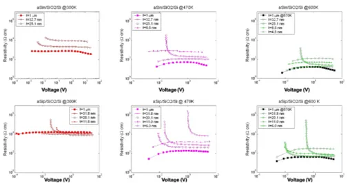
amor-phous layer as a function of temperature, measured with a constant heating rates (dT/dt) of 15 K/min. The inset shows the thickness of each layer. . . 27 1.12 Sheet resistance of n-doped (a-b-c) and p-doped (d-e-f) amorphous
layer, measured with constant temperature reported of 300K (a, d), 470K (b, e) and 600K (c, f). The inset shows the thickness of each layer. . . 28 1.13 Curves for the optical absorption coefficient as a function of Energy,
for p-doped (blue line), intrinsic (black line), and n-doped (green line) amorphous silicon layer. (courtesy of dott. Salvo Mirabella) 29 1.14 Simulations of the absorbed power of a PIN diode (a)with 1 um of
absorber (intrinsic layer) and by varying the top contact thickness from 10 to 40 nm and (b) using a 20 nm of window layer thickness and by varying the absorber layer thickness The black curve shows the AM 1.5 G incident spectrum. . . 30 1.15 Simularion of the impact of D-centers on the PV cell performance.
(Courtesy of Dott. Cannella). . . 32 1.16 The table reported the thickness of the analyzed diode. Schematic
sketch of the realized p-i-n thin film solar cell. . . 34 1.17 Current voltage (a) and current density voltage (b-d) characteristics
of several Pin diodes, analyzed in dark condition. The sample was made by varying the thickness of the absorber layer from 1 �m to 125 nm. The diameters of the analyzing diode are showed in the inset. . . 35 1.18 Courtesy Dott.ssa M. Foti (ST) . . . 37
2.1 Figure 1. Variation of deposition rate as a function of hydrogen dilution of silane for a-Si:H and nc-Si:H films deposited by PE-CVD withFSiH4=100 sccm (red) and FSiH4==12 sccm(blue). . . 44
2.2 Plan view dark field TEM micrographs obtained by selecting the s[26]pot <111> for the hydrogenated Si layers deposited using FSiH4=12
sccm and R=10(a) R=20(b) R30(c) R40(d). The films present a high density of nanocrystalline dots. . . 46 2.3 a) The scattered intensity I(q) (red line), for the sample deposited
using FSiH4=12 sccm and R=10, the dashed line represent the back-ground , calculated by fitting with a polynomial curve of II degree. The inset shows the diffraction pattern from which we collected I(q), (b) Calculated φ(q).The vertical lines indicate the range chosen for the calculation of G(r). . . 48 2.4 Pair distribution function, G(r ), of the a-Si:H film for the several
flow values R. The samples were made by using 100 sccm of silane flow (dashed line) with R=2 (black curve), R=10(red curve), and 12 sccm SiH4 flow (continuous line) with R=10 (green curve), R=20
(magenta curve), R=30 (cyan curve) and R=40 (blue curve). The G(r) of a-Si:H evolves towards that of c-Si and begins to exhibit peaks that correspond to the higher crystalline coordination shells. The vertical lines indicate the peak positions in the g(r) of c-Si. . . 49 2.5 Hydrogen concentration for sample made by PECVD using different
silane flow 100 sccm (black circle), and 12 sccm (black square) and different Hydrogen dilution(R). . . 51 2.6 Figure 6. Schematic representing the local structural
rearrange-ments of Si atoms (blue spheres) before (a) and after(b) interaction with hydrogen atom (red spheres . The Si-Si bonds are indicated for the equilibrium bond lenght 2.35 Å by the blue line, and for the ones under tensile or compressive strain by red lines or green line respectively. The superposition of the black dots that indicate the c-Si lattice positions onto the Si cluster structure, obtained after many H interaction events, shows that the rearranged atomic po-sitions in the Si cluster correspond well with the equilibrium c-Si lattice sites. . . 52 2.7 .(a) FTIR transmission spectra for silicon hydrogenated layer
de-posited with the different R=H2/SiH4 ratios, as listed in the
leg-end on the right of the Figure, and (b) FTIR experimental data for the same sample as in a) for the 1850-2250 cm-1 range, after the background subtraction. . . 54
the sample R=10 FSiH4=12 sccm,(a) and Hydrogen content of the
films obtained by ERDA (b) as a function hydrogen dilution, and normalised respect to the same sample. . . 55 2.9 FTIR experimental data for the several samples (graph (a) to (f)),
and results of the gaussian deconvolution, by using the frequen-cies listed in table 1 relative to SiH, SiH2 and SiH3. The vertical
thin lines represent the position of these literature values for the stretch vibrational modes of SiH(2000 cm−1), SiH
2(2090 cm−1),
SiH3(2140cm−1). The blue curves represent the raw data, while
red curves represent the convolution of the three components. . . 57 2.10 Si-H3 bonded species correlated with the SiH bonding, for several
sample. The triangles represent the layer deposited with FSiH4=100
sccm, while the square represent the layer sequence deposited with FSiH4=12 sccm. . . 58
2.11 TEM Micrograph in bright field condition of R=20 sample, showing the Silicon substrate (dark grey region), the SiO2 substrate (light
grey region=) and the deposited Si:H layer, which shows a poly-columnar morphology in the upper part of the layer. (b) Mean size of nanostructure at various R for samples deposited withFSiH4
=12 sccm, obtained through plan view TEM analysis in Dark field condition. The data represent the mean radius of the dots present in the surfacial region of the Si:H layer. . . 59 2.12 TEM Micrograph in bright field condition of R=40 sample, showing
white regions, evidenced by the arrows, that represent the nanovoids created by hydrogen, and appear in correspondence of the grain boundaries. . . 60
3.1 (a) SEM Micrograph in tilted view (30° along the y axis) of the nanoporous SiO2template realised by nanopatterning based on
di-block copolymer self-assembly. The analysis was performed on the cleaved edge of the sample. It is possible to identify the Si substrate in the bottom and the etched oxide layer on top. (b) Cross-section TEM image of a sample: it is visible the 15 nm oxide layer etched down to the Si substrate for about 8 nm. The black line shows the typical etch profile in the oxide layer of the samples. The total pore depth is about 23 nm and the curvature radius at the bottom of the nanopores is about 6 nm.[26] . . . 71
3.2 Bright field TEM micrograph of a templated oxide substrate af-ter sputaf-tering of gold nanodots. The white regions represents the nanopores in the SiO2 substrate and the black dots represent the
gold nanodots deposited randomically on the substrate.[26] . . . . 72 3.3 TEM micrographs in plan view of the nanopatterned oxide
sub-strates of, after deposition of Au dots and annealing for 1 hour at 600 °C (a) and 800 °C (b). In a) it is possible to see the nanopores in the SiO2 substrate and the randomic Au nanodots (dark spots), while in b) the ordered Au dots saturating the nanopores together with few dots outside the nanopores.[26] . . . 74 3.4 Gold dot radius distributions in the as deposited samples (circles)
and for the samples annealed for 1 hour at 600 °C (squares), 800 °C (diamonds) and 1000 °C (triangles).[26] . . . 75 3.5 Au dot density (a), diameter (b) and coverage (c) for the as
de-posited samples (circles) and for the samples annealed for 1 hour at 600 °C (squares), 800 °C (diamonds) and 1000 °C (triangles).[26] . 77 3.6 (a) SEM images in plan view of the nanopatterned oxide substrates
after the deposition of Au dots and annealing at 1000 °C for 1h. It is possible to see the nanopores in the SiO2substrate (black circles)
and the gold nanodots diffused in the nanopores (white spots).(b) Cross-section TEM micrograph of the sample show one nanopore completely filled with the gold and some empty pores close to it.[26] 78 3.7 (a) The Gibbs free energy differential as a function of volume and
surface term for a cluster on a surface, and (b) schematic illustrat-ing the Young-Duprè equation for the surface and Interface tension terms for a cluster in its equilibrium shape with a contact angle[33] 80 3.8 a) Sketch of the cluster’s evolution, the red arrow indicate the
adatoms that leave the cluster with size R<R* and adatoms that diffuse toward the cluster with R>R*due to the adatoms concen-tration gradient. b) Superposition of concenconcen-tration distance and energy distance diagram for two dimensional cluster on a surface, showing the different energy levels involved in cluster growth[33] . 82 3.9 Experimental value of Ds for the SiO2 substrate(triangles) as a
function of T−1with the relative Arrhenius fit (continuius line) [42].
The inset is a scale picture which rapresents our pattern where the blue circle are the pores and the gold sphere are the cluster, the pink shape represents the aspected diffusion area after 1 hour of annealing . . . 83
pores are evidenced by the white dashed circles, and identified as P1, P2 and P3. The black shapes highlight several groups of dots
which diffuse on the substrate and/or toward the pore. A group of Au dots which diffuse toward one of the nanopores of the substrate are identified by number 1 to 7 . The ripening of some groups of Au dots identified by α, β and γ is evidenced by the black arrows (a), (b) and (c). . . 85 3.11 TEM micrograph in plan view of the nanopatterned oxide substrate
after deposition of Au dots and annealing for 1 hour at and 800 °C. It is possible to see the Au NDs in correspondence of the nanopores underneath, arranged in the hexagonal configuration, as evidenced by the red hexagons. . . 86
List of Tables
1.1 list of parameters and respective values used in our simulations. . . 31 2.1 Si-H vibrational modes [31] . . . 53
Introduction
0.1 General overview
Photovoltaic technology has received increased attention as one of the most promis-ing approach to carbon-free energy production. Bulk silicon cells, which convert between 14 and 17% of incident light into electricity, make up 90% of the solar cell market. Silicon is widely used because it is the second most abundant element in the earth’s crust, and because the electronics industry has already developed infrastructure to process it. Yet the pricey and complicated manufacturing makes these photovoltaic (PV) systems more expensive per kW/h than conventional en-ergy sources. These limitations have driven efforts to develop inexpensive solar modules with efficiencies equivalent to, or better than, existing devices. Thin films solar cells are widely recognized as a key solution to reducing the manufacturing cost of PV cells in the near to medium term. Thin film solar cells are able to be produced at low cost by removing the bulk active substrate and using an additive deposition process on top of a low cost substrate such as glass, metal foil, plastic, etc. Compared with other thin-film solar cell technologies, thin-film silicon has the advantage of constituting an industrially mature technology and of being based on raw materials which are present in abundance in the earth’s crust.[1] During the last three decades, hydrogenated amorphous silicon has been studied extensively as basic material for thin film solar cells due to the natural abundance of source ma-terial, environmental safety, potential high performance and the capability of low cost production. However, the defect density of hydrogenated amorphous silicon (a-Si:H) increases with light exposure, to cause an increase in the recombination current and leads to the reduction in the sunlight to electricity conversion effi-ciency. This phenomenon is known as Staebler-Wronski effect [2] For this reason, the solar cells based on a-Si:H have always been associated with efficiency losses due to the light-induced degradation over the time. For amorphous silicon the photoinduced degradation due to the creation of dandling bond defect has been the most important issue for improving the efficiency [3] Extensive research has been carried out by many laboratories to improve the conversion efficiency of
a-Si:H solar cells [4]. In this thesis an intensive study on thin film a-a-Si:H solar cells will be shown.The fundamental photodiode inside an amorphous silicon–based so-lar cell has three layers deposited in either the p-i-n or the n-i-p sequence. The realization of a pin solar cell will be shown, including the investigation of the key physical properties necessary to design the solar cell (sheet resistance, activation energies for conductivity, light absorption). The electrical characteristics of the solar cells in dark condition and under standard illumination will be presented and compared to the theoretical models.
In order to make photovoltaic technology cost effective we need to improve the efficiency and minimize the light induced degradation of photoconductivity caused by Staebler–Wronski effect [2]. A material that presents very promising features is hydrogenated nanocrystalline silicon (nc-Si:H)[15]. The nc-Si:H is made using PECVD,
In order to make photovoltaic technology cost effective we need to improve the efficiency and minimize the light induced degradation of photoconductivity caused by Staebler–Wronski effect. A material that presents very promising features is hy-drogenated nanocrystalline silicon (nc-Si:H). The nc_Si:H is made using PECVD, using a gas mixutre of SiH4 and H2, the cristalline dimension can be tailored
by variyng the hydrogen dilution of Silane in PECVD camera. The transition from amorphous to nanocrystalline silicon is induced by Hydrogen. Vettel et al [5]demonstrated an important result, the deposition condition near the transition between amorphous an cristalline growth have been found to be the most beneficial to the solar cells properties. Nc-Si:H films show stability under light soaking, sug-gesting that the disorder in the amorphous Si network plays a major role, and thus Nc-Si:H have high potential as stable solar cell material. The parameter that could play a role in the stability under light soaking and also in the crystalline fraction is believed to be the hydrogen concentration and its complex bonding mechanism. The major technical challenge with such nanocrystalline solar cells is the fact that the surface area of grain boundaries is very high, significantly increasing the den-sity of recombination centers as well as the probability of recombination due to charge carriers having to pass through so many boundaries, indicating that the crystalline fraction and the grain size of these materials determine also the elec-trical properties of the final device. It is believed that the hydrogen content and its complex bonding behavior is the responsible for the structural characteristics and as a consequence for the stability under illumination. In order to control the optical and electrical properties and then the stability under light soaking effect, the hydrogen contribution must be deeply understood. In this thesis a study of the morphological behaviors of nc-Si:H films as a function of the hydrogen content will be showed. Nc-Si:H thin films were deposited by ST microelectronics under different conditions by PECVD deposition by varying the ratio H2/SiH4 flow.
The variation of morphology and hydrogen content was studied in detail, using
Cr is ti na A nn am ar ia G ar oz zo ,P hD Th es is in M at er ia lS ci en ce ,U ni ve rs it y of Ca ta ni a, 2010
0.1. General overview
TEM analysis, ERDA and FT-IR measurements. The study of this material was also made using the radial distribution function (RDF), which starting from the diffraction pattern of TEM analysis, gives the number of atoms at a given distance from a central atom. The contribution of the hydrogen in the transition from an a-Si:H layer, with low R, to a nc-Si:H layer, with high R, will be demonstrated.
As previously described, in contrast to amorphous silicon (a-Si), nc-Si exhibits high stability against photo-induced degradation. However, nc-Si thin-film solar cells require an intrinsic layer of 2–3 �m in thickness to absorb sufficient amount of sunlight due to its indirect optical transition. For this reason in literature an-other type of nanostructure, has been recently proposed, the Si nanowires. Silicon nanowires offer several performance and manufacturing benefits that may impact future PV applications. Their main advantage is based on the fact that they orthogonalize the pathways for light absorption and carrier collection. Recently Atwater et al. reported the potential of radial p-n junction wire array solar cells, which consist of a dense array of semiconducting wires, each having a p-n junction in the radial direction, and oriented with the nanowires axis parallel to the inci-dent light direction. By fabricating p-n junctions conformally around the wires structure, in a radial configuration, the absorption of light can be decoupled from minority carrier diffusion. This approach is useful to the creation of efficient solar cells using low lifetime materials. [7, 1]. Although fabrication of wires in microm-eter sized dimension have been proposed in many works to prevent the surface recombinarion, the approach proposed in this thesis is the use of nanometer sized dimention to the nanowires syntesis. The choice of using these nano-structures is driven by numerous factors. The possibility of a switch to an almost direct gap with the ability to vary the energy gap by varying the diameter of the wires is one of the main factors. Zhao et [10]found that for a nanowires oriented in [100] direction with diameter of about 6-8 nm the resulting energy gap is about 1.4 eV. This result is very close to the Shockley–Queisser limit[?]. The theoretical maxi-mum almost corresponds to the GaAs band gap. ( 1.42 eV), However, due to high production costs GaAs is reserved for solar applications, for this reason in very interesting the use of a technique that is able to achieve an Eg of 1.4 with low cost production. There are two basic approaches of synthesizing nanowires: top-down and bottom-up approach. A top-down approach combines lithographic steps or etching process to produces nanowires from a flat surface. The major drawback of the top-down method is that the surfaces of the structure are damaged during the process resulting in nanowires with a poor crystal quality. In addition the lithographic techniques may not be able to produce sufficiently small structures for further downscaling of devices. In order to produce small enough nanowires of high enough crystal quality, the bottom-up approach is thought to be a potential alternative. The idea is to build-up nanosized structures and devices by using nanoscale building blocks to initiate growth directly at desired positions and with
Cr is ti na A nn am ar ia G ar oz zo ,P hD Th es is in M at er ia lS ci en ce ,U ni ve rs it y of Ca ta ni a, 2010 .
designed dimensions and properties. In contrast to the lithographic and etching techniques used in the top-down methodology, the bottom-up approach involves the direct growth of one-dimensional nanostructures onto a substrate. The typi-cal method to fabricate NWs by bottom-up approach is the catalytic growth with random metallic nanoparticles. A better understanding of the catalytic nanowire growth process is necessary to pin down the growth mechanism and to be able to rationally control their compositions, sizes, crystal structures, and growth direc-tions. Gold was used as a catalyst for the nucleation of the Si nanophase. The choice to use gold relies on the advantages of this metal respect to others, like Ni, Sn, Al and Cu, such as its low eutectic temperature with Si, the opportunity to eas-ily form alloys with the growth precursor and the fast inter-diffusion of Si through gold nanodot. Gold, however, presents some drawbacks, because it creates deep band gap defects and for this reason the data shown represent a proof of concept, and alternative metals must be investigated for device integration. The catalytic growth of silicon nanowires is commonly described either by the vapor-liquid-solid (VLS) or solid-liquid-solid (SLS) process. The VLS process was first suggested by Wagner and Ellis [11]who showed that micrometer-scale silicon whiskers could be grown from metal droplet catalysts under Chemical Vapor Deposition conditions at about 1000 °C. A typical VLS mechanism starts with the dissolution of gaseous precursors (SiH4 or SiH2Cl2) into nanosized liquid alloy (metal Au-Si) droplet
considered as a catalytic site. Once the liquid droplet is supersaturated with sili-con, then the precipitation of solid nanowire occurs. The process was named the VLS beacuse of the three phases involved. In this method, metallic nanoparticles are deposited randomically on a Si substrate and work as catalysist seeds for the nucleation of the Si phase from the vapor source, in the first case, and from the substrate source, in the second case. During the growth, in both cases however, some lateral diffusion of the metallic dots on the substrate can produce a coales-cence of the metal nano-seeds, thus increasing the disorder level in the template substrate, and producing a final “forest-like” material. Therefore, when position control of spatially separated NWs is desired, nanopatterning techniques become essential. Some approaches have been demonstrated, or are potentially applicable, for position and size control of semiconductor NWs. [11] A number of patterning and templating methods can be applied for the controlled preparation of metal dots or metal-dot arrays on a substrate surface, including photo- or e-beam lithog-raphy, manipulation of single gold nanodots, arrangement of Au nanocrystals from suspensions, nanosphere lithography, gold deposition masks based on porous alu-mina templates, nanoimprint lithography, as well as other catalyst-positioning approaches. Since the final structural and geometrical characterisitcs of the NWs are strictly correlated to the catalyst dot properties, we want to control the cat-alytic seed characteristics, such as shape, position, dimension and we create a SiO2
barrier to the lateral diffusion during the annealing to control the final nanowires
Cr is ti na A nn am ar ia G ar oz zo ,P hD Th es is in M at er ia lS ci en ce ,U ni ve rs it y of Ca ta ni a, 2010
0.2. Thesis outline
template. In this thesis we propose an approach to obtain these characteristics based on a two steps process. i) First of all the formation of a polymeric nanomask by diblock copolymer self-assembling [13, 14, 15] and successive dry etch to trans-fer the polymeric pattern on the oxide substrate [16, 17, 18, 19, 20]. This creates an ordered array of nanopores of controlled size and density and position. The obtained substrate is made of a silicon dioxide layer with nanopores 20 nm wide and separated by a 40 nm distance, etched down to the Si substrate. ii) After-wards, catalyst nanodots was deposited and diffused over the template. A single layer of gold NDs, with coverage 20%, is deposited by sputtering all over the tem-plate, and subjected to thermal annealing at temperatures ranging between 600 and 1000 °C, to diffuse the metallic NDs on the surface. In this thesis it is shown that the NDs deposited randomically over the template either inside and outside the pores, during the annealing diffuse and coalesce randomly over the substrate, but in correspondence of the nanopores they stop the diffusion, probably due to the presence of some surfacial defects. The final result of this process is that most of the nanopores are saturated with the gold NDs. The density of saturated nanopores can be tuned by changing the annealing temperature. The preferential diffusion of the gold NDs toward the nanopores is followed in situ by annealing the samples during TEM imaging, and ex-situ by annealing in furnace the samples and observing them by TEM and high-statistics SEM analysis.
0.2 Thesis outline
The first chapter describes the pin cells realization. To explain the characteristic of hydrogenated amorphous silicon in the first section, we introduce some of the fundamental physical concepts required to interpret the scientific literature about amorphous silicon.The second section describes the electrical and optical char-acterization of the layer that compose the solar cells, and an accurate electrical characterization of the pin structure realized by ST.
The second chapter shows the characterization of nc-Si:H thin films made by PECVD for solar cells. In particular a structural characterization performed by TEM analysis will be showed, and the role of hydrogen in the transition from a-Si:H to nc-Si:H will be deeply analyzed and discussed.
The third chapter shows results on the fabrication of ordered nanowires. It uses an alternative lithography based on diblock copolymer self-assembling which generates ordered arrays of nanopores of controlled size, density and position. This can be used as a template for the catalytic mediated growth of controlled nanowires. Cr is ti na A nn am ar ia G ar oz zo ,P hD Th es is in M at er ia lS ci en ce ,U ni ve rs it y of Ca ta ni a, 2010 .
Cr is ti na A nn am ar ia G ar oz zo ,P hD Th es is in M at er ia lS ci en ce ,U ni ve rs it y of Ca ta ni a, 2010
References
[1] L. Tsakalakos. Materials Science and Engineering R 62 (2008) 175–189 [2] Staebler, D. L.; Wronski, C. R. Applied Physics Letters , vol.31, no.4,
pp.292-294, Aug 1977 doi: 10.1063/1.89674
[3] Kondo et. al. Thin solid films 501 (2006) 243-264.
[4] [4] Funde et al. Solar Energy Materials & Solar Cells 92 (2008) 1217– 1223. [5] O. Vetterl, F. Finger, R. Carius, P. Hapke, L. Houben, O. Kluth, A. Lam-bertz, A. MuKck, B. Rech, H. Wagner. Solar Energy Materials & Solar Cells 62 (2000) 97}108
[6] A. V. Shah, H. Schade, M. Vanecek, J. Meier, E. Vallat-Sauvain, N. Wyrsch, U. Kroll, C. Droz and J. Bailat. Prog. Photovolt: Res. Appl. (2004); 12:113–142
[7] B.M.Kayes, H.A. Atwater N.S. Lewis. J. Appl. Phys. 97, 114302 (2005).. [8] Tsakalakos Appl. Phys. Lett. 91 233117(2007).
[9] W. Shockley, H.J. Queisser, J. Appl. Phys. 32 (1961) 510.
[10] Xinyuan Zhao, C. M. Wei, L. Yang, and M. Y. Chou. PHYSICAL REVIEW LETTERS 92(23),236805 (2004)
[11] R.S. Wagner, W.C.Ellis: Vapor- Liquid-Solid Mechanism of single crystal growth. Appl Phys Lett . 4, 89-90 (1964).
[12] H.J. Fan, P. Werner, M. Zacharias: Semiconductor Nanowires: From Self-Organization to Patterned Growth. Small. 2:700-17 (2006).
[13] K.W. Guarini, C.T. Black, S.H.I. Yeung: Optimization of Diblock Copoly-mer Thin Film Self Assembly. Adv. Mater. 14 (18), 1290 (2002).
[14] T. Thurn-Albrecht, J. Schotter, G.A. Kastle, N. Emley, T. Shibauchi, L. Krusin-Elbaum, K. Guarini, C.T. Black, M. T. Tuominen, T. P. Rus-sell: Ultrahigh-Density Nanowire Arrays Grown in Self-Assembled Diblock Copolymer. Templates.Science. 290, 2126 (2000)
[15] I.A.Zucchi, E.Poliani and M.Perego: Microdomain orientation dependence on thickness in thin films of cylinder-forming PS-b-PMMA. Nanotechnology 21 (2010) 185304
[16] S.J. Kim, W.J. Maeng, S.K. Lee, D.H. Park, S.H. Bang, H.Kima, B.H. Sohn: Hybrid nanofabrication processes utilizing diblock copolymer nanotemplate prepared by self-assembled monolayer based surface neutralization. J. Vac. Sci. Technol. B 26(1), 189-194 (Jan/Feb 2008).
[17] K.W. Guarini, C.T. Black, Y. Zhang, H. Kim, E.M. Sikorski, I.V. Babich: Process integration of self-assembled polymer templates into silicon nanofab-rication. J. Vac. Sci. Technol. B, 20(6), 2788-2792 (2002).
[18] K.W. Guarini, C.T. Black, K.R. Milkove, R.L. Sandstrom: Nanoscale pat-terning using self-assembled polymers for semiconductor applications. J. Vac. Sci. Technol. B.19( 6), 2784-2788 (2001).
[19] P. La Fata, R. Puglisi, S. Lombardo, C. Bongiorno: Nano-patterning with Block Copolymers. Superlattices and Microstructures. 44 693–698 (2008). [20] R.A. Puglisi, A. Scandurra, C. Bongiorno, P. La Fata and S. Lombardo:
Pattern transfer of nanomasks based on diblock copolymers through Reactive Ion Etching ( to be submitted).
Cr is ti na A nn am ar ia G ar oz zo ,P hD Th es is in M at er ia lS ci en ce ,U ni ve rs it y of Ca ta ni a, 2010
Chapter 1
aSi:H Thin Film solar cells
1.1 Introduction
Silicon is the semiconductor of choice in Photovoltaic Industry. In fact, silicon is abundant, environmentally inert and is one of the technically and scientifically most advanced materials. However, standard silicon photovoltaic technology suf-fers from several drawbacks: the processes are energy consumptive, too much material is wasted during processing, the cells are -for technical limitations- much thicker than what would be needed, and large area and module fabrication is awkward[2, 1]. On the other hand, conversion efficiencies are high and as men-tioned above, the technology is well advanced. Therefore, it has ever been the challenge to improve on those drawbacks while keeping the silicon advantages. One way is the so-called thin film silicon solar cell. There are two forms of thin-film silicon material that can be used for constituting such a solar cell: hydrogenated amorphous silicon (a-Si:H) and hydrogenated microcrystalline silicon (µc-Si:H) or hydrogenated nano-crystalline silicon (nc-Si:H). With this device one wants to reduce film thickness to what is a minimum needed for complete solar light ab-sorption, reduce process temperatures in order to use low-cost substrate materials and use processes which allow large area fabrication and integration into modules. Such thin-film silicon solar cells require a far lower amount of silicon material than the ‘classical’ wafer- based crystalline silicon solar cells; this means that they have, on a medium-term time scale, a more pronounced cost reduction potential than the latter. Furthermore, the ‘energy payback time’, i.e., the time required for the photovoltaic solar module to ‘pay back’, to the user, the quantity of energy in-vested during its fabrication, is at least a factor of two lower in the case of thin-film silicon solar cells than for wafer-based crystalline silicon solar cells: this may, in the long run, turn out to be a decisive factor. Compared with other thin-film solar
cell technologies, thin-film silicon has the advantage of constituting an industrially mature technology and of being based on raw materials which are present in abun-dance in the earth’s crust. Their stabilized efficiency is, however, at this moment still rather limited, for reasons which we will see later in this chapter in section 1.3.3. This is where hydrogenated nanocrystalline silicon (nc-Si :H) prepared by plasma-enhanced chemical vapour deposition (PECVD) enters [2, 1]. Being in the field for long in amorphous silicon-based devices as highly conductive contact layer, recently much progress has been made to control the process of fabrication in order to achieve improved deposition rates and high electronic quality such that now nc-Si :H can be used as active layer in solar cells [3, 4, 5, 6]. This chapter is organized as follows. The first section describes how the simplest, single-junction solar cell “works,” by which we mean how the photoelectric behavior of the cell is related to the fundamental concepts. After this we introduce the hydrogenated amorphous silicon the deposition technique and some of the fundamental physical concepts required to interpret the main characteristics of the hydrogenated amor-phous silicon materials. The drawbacks related to the Staebler-Wronsky effect are shown in the section1.3.3, and some solutions such as the nanocrystalline silicon are presented later in the chapter. The results and discussion section reports the activity performed by us of thin films deposition and characterization, pin PV cell design and pin PV cell realization and characterization
1.2 Semiconductor Solar cells.
Semiconductor solar cells are quite simple devices. Semiconductors have the ca-pacity to absorb light and to deliver a portion of the energy of the absorbed pho-tons to carriers of electrical current –electrons and holes. A semiconductor diode separates and collects the carriers and conducts the generated electrical current preferentially in a specific direction.[7] Thus, a solar cell is simply a semiconductor diode that has been carefully designed and constructed to efficiently absorb and convert light energy from the sun into electrical energy. A simple conventional solar cell structure is depicted in Figure 1.2 Sunlight is incident from the top on the front of the solar cell. A metallic grid (indicates by the arrow in fig 1.1 ) forms one of the electrical contacts of the diode and allows light (orange arrows) to fall on the semiconductor between the grid lines and thus be absorbed and converted into electrical energy. An antireflective layer (Anti Reflection Coating, ARC) (indicates by the arrow in fig. 1.1 a) between the grid lines increases the amount of light transmitted to the semiconductor. The semiconductor diode is fashioned when an n-type semiconductor and a p-type semiconductor are brought together to form a metallurgical junction. This is typically achieved through dif-fusion or implantation of specific impurities (dopants) or via a deposition process. The diode’s other electrical contact is formed by a metallic layer (purple zone)on
Cr is ti na A nn am ar ia G ar oz zo ,P hD Th es is in M at er ia lS ci en ce ,U ni ve rs it y of Ca ta ni a, 2010
1.2. Semiconductor Solar cells.
Figure 1.1: A schematic of a simple conventional solar cell. Creation of elec-tron–hole pairs, blue circle and red circle, respectively, is depicted
the back of the solar cell.
In the following section a discussion on the key electrical parameter to charac-terize solar cells is reported.
1.2.1 Solar Cell I –V Characteristics
Equation (1) is a general expression for the current produced by a solar cell.
(1)
The short-circuit current and dark saturation currents are given by rather complex expressions [7] that depend on the solar cell structure, material properties, and the operating conditions. A full understanding of solar cell operation requires detailed examination of these terms. However, much can be learned about solar cell operation by examining the basic form of equation (1). From a circuit perspective, it is apparent that a solar cell can be modeled by an ideal current source (ISC) in
parallel with two diodes, the first with an ideality factor and the the other with an ideality factor of “2”, as shown in Figure1.2 a) .
Cr is ti na A nn am ar ia G ar oz zo ,P hD Th es is in M at er ia lS ci en ce ,U ni ve rs it y of Ca ta ni a, 2010 .
Figure 1.2: Simple solar cell circuit model. Diode 1 represents the recombina-tion current in the quasi-neutral regions (∝ eqV /kT ), while diode 2 represents
recombination in the depletion region (∝ eqV /2kT)(b)[7]
Figure 1.2 b) shows the current – voltage (I – V ) characteristic of a typical silicon solar cell. For simplicity, the dark current due to the depletion region (diode 2) has been ignored (a reasonable and common assumption for a good silicon solar cell, especially at larger forward biases). From The figure 1.2 b illustrates key parameter of solar cells – the short-circuit current Isc, the open-circuit voltage
VOC, and the fill factor FF. At small applied voltages, the diode current is negligible
and the current is just Isc, as can be seen when V is set to zero in equation (1).
When the applied voltage is high enough so that the diode current (recombination current) becomes significant, the solar cell current drops quickly. At open circuit (I = 0), all the light-generated current, Isc, is flowing through diode 1, so the
open-circuit voltage can be written as
(2) where IS C � Io1.
the maximum power point PM P ≡ (VM P,IM P),i.e. is the point on the I–V
curve where the power produced is at a maximum. As seen in Figure 1.2b this point defines a rectangle whose area, given by PM ax = VM PIM P, is the largest
rectangle for any point on the I –V curve. The maximum power point is found by solving Cr is ti na A nn am ar ia G ar oz zo ,P hD Th es is in M at er ia lS ci en ce ,U ni ve rs it y of Ca ta ni a, 2010
1.2. Semiconductor Solar cells.
(3)
for V = VMP. The current at the maximum power point, IMP, is then found by evaluating equation (1) at V = VM P.
Another important characteristic is the fill factor, FF, which is a measure of the squareness of the I–V characteristic and is always less than one. It is the ratio of the areas of the two rectangles shown in Figure 1.2 b) or
(4)
Obviously for a solar cell the power conversion efficiency, η, is the most impor-tant parameter to analyze; η is defined as
(5)
The incident power, Pin, is determined by the properties of the light spectrum incident upon the solar cell. In the following section the light spectrum property will be discussed.
1.2.2 Air Mass
The sun has a surface temperature of 5762 K and its radiation spectrum can be approximated by a black-body radiator at that temperature. Emission of radiation from the sun, as with all black-body radiators, is isotropic. However, the Earth’s great distance from the sun means that only those photons emitted directly in the direction of the Earth contribute to the solar spectrum as observed from Earth. Therefore, for practical purposes, the light falling on the Earth can be thought of as parallel streams of photons. Just above the Earth’s atmosphere, the radiation intensity, or Solar Constant, is about 1.353 kW/m2[8] and the spectral distribution
is referred to as n air mass zero (AM0) radiation spectrum. The Air Mass is a measure of how absorption in the atmosphere affects the spectral content and intensity of the solar radiation reaching the Earth’s surface. The Air Mass number is given by AirMass = 1/cosθ where θ is the angle of incidence (θ = 0 when the sun is directly overhead). A widely used standard for comparing solar cell performance is the AM1.5 spectrum normalized to a total power density of 1 kW/m2 . The
Cr is ti na A nn am ar ia G ar oz zo ,P hD Th es is in M at er ia lS ci en ce ,U ni ve rs it y of Ca ta ni a, 2010 .
spectral content of sunlight at the Earth’s surface also has a diffuse (indirect) component owing to scattering and reflection in the atmosphere and surrounding landscape and can account for up to 20% of the light incident on a solar cell. The Air Mass number is therefore further defined by whether or not the measured spectrum includes the diffuse component. An AM1.5g (global) spectrum includes the diffuse component, while an AM1.5d (direct) does not . [7]
1.3 Hydrogenated amorphous silicon
Hydrogenated amorphous Si is deposited from hydride gases such as SiH4 using
plasma to decompose the gas. This is called plasma-enhanced CVD (PECVD) and allows for large areas to be coated rather uniformly and with excellent con-trol. However, the utilization of gases is only around 10 to 30%, meaning much of the source material is wasted. The material has 1 to 10% hydrogen bonded to the Si, and is often designated as a-Si:H. The H atoms passivate a large number of the defects resulting from the incomplete bonding of the Si atoms. The atomic structure has no long-range order like all other crystalline or polycrystalline ma-terials. This will be deeply analyzed in chapter 2. This can be an advantage. Films are typically deposited between 150 to 300°C, this temperature conditions allowing the use of lower-cost, low-temperature substrates like glass, stainless steel foil, or plastic. The pn junction is formed by doping the thin contact layers as they grow with dopant gases containing the boron or phosphorous atoms. In the following section will be discussed how the PECVD works. And after, to explain the characteristic of hydrogenated amorphous silicon in the following section we briefly introduce some of the fundamental physical concepts required to interpret the scientific literature about amorphous silicon.
1.3.1 PECVD
As as above-mentioned a-Si:H is deposited from hydride gases such as SiH4using
plasma to decompose the gas. Figure?? shows a schematic of a typical RF PECVD chamber and related parts. A silicon-containing gas such as a mixture of SiH4
and H2flows into a vacuum chamber that is evacuated by a pump. Two electrode
plates are installed inside, and an RF power is applied between them; one option is to ground one of these electrodes. At a given RF voltage across the plates, there is usually a range of gas pressures for which a plasma will occur. The plasma excites and decomposes the gas and generates radicals and ions in the chamber. Various substrates may be mounted on one or both of the electrodes, and thin hydrogenated silicon films grow on the substrates as these radicals diffuse into them. The substrates are heated to achieve optimum film quality; this effect is attributed to thermally activated surface diffusion of adatoms on the growing film.
Cr is ti na A nn am ar ia G ar oz zo ,P hD Th es is in M at er ia lS ci en ce ,U ni ve rs it y of Ca ta ni a, 2010
1.3. Hydrogenated amorphous silicon
Figure 1.3: Schematic of a typical RF glow discharge deposition chamber[15]
A PECVD system usually consists of several major parts (shah):
1)a gas delivery system (gas cylinders, pressure regulators, mass flow con-trollers, and various gas valves to direct gas flows);
2) a deposition chamber that has electrodes, substrate mounts, substrate heaters, and the RF power feed through;
3)a pumping system that usually has a turbomolecular pump backed with a mechanical pump;
4) a pressure control system that has a capacitance manometer, ionization gauges, thermocouple gauges, and/or throttle valve to monitor and control the chamber pressure;
5)an exhaust system for the process gases (typically either with a chemical scrubber to neutralize the gases or with a “burn box” to pyrolyze them).
The film growth in a PECVD process consists of several steps: source gas dif-fusion, electron impact dissociation, gas-phase chemical reaction, radical diffusion, and deposition [11, 9, 10]. To deposit good-quality a-Si films, the deposition con-ditions need to be controlled within certain ranges desirable for high-quality a-Si growth.
The pressure range is usually between 0.05 and 2 Torr. Lower pressure is desirable for making uniform deposition, and higher pressure is more desirable for preparing microcrystalline silicon films. Most researchers use a pressure between 0.5 and 1 Torr for a-Si deposition. The RF power should be set at around 10 to 100 mW/cm2 for a capacitively coupled reactor. Below 10 mW/cm2, it is difficult to
maintain a plasma. Higher power is desirable for higher deposition rate. However, above 100 mW/cm2, the rapid reactions in the gas can create a silicon polyhydride
powder that contaminates the growing Si film. This problem can be mitigated by using very low pressure or strong hydrogen dilution. The substrate temperature
Cr is ti na A nn am ar ia G ar oz zo ,P hD Th es is in M at er ia lS ci en ce ,U ni ve rs it y of Ca ta ni a, 2010 .
is usually set between 150 and 350°C. At lower substrate temperature, more H is incorporated in the film.
1.3.2 Characteristics of a-Si:H
Silicon atoms in amorphous silicon largely retain the same basic structure as that of crystal silicon: each silicon atom is connected by covalent bonds to four other silicon atoms arranged as a tetrahedron. Moreover, not all the atoms within amorphous silicon are fourfold coordinated. Due to the disordered nature of the material some atoms have a dandling bond. Physically, these dandling bonds represent defects in the continuous random network and may cause anomalous electrical behavior. For hydrogenated amorphous silicon (a-Si:H), silicon–hydrogen bonds resolve this structural problem. Several percent of the silicon atoms make covalent bonds with only three silicon neighbors; the fourth valence electron of the silicon bonds to a hydrogen atom. There are quite a few distinct atomic configurations for the hydrogen in a-Si:H. The two principal “phases” of hydrogen evidenced by proton magnetic resonance are termed the dilute and clustered phases [12]. In the dilute phase a particular hydrogen atom is about 1 nm away from any other hydrogen atom; in the clustered phase there are two or more hydrogen atoms in close proximity. A computer calculation of a particular instance of this structure [13] is presented in Figure 1.4. The densities of hydrogen in each of the individual phases, as well as the total density of hydrogen, depend upon the conditions under which the material is made.
While the underlying structure illustrated in Figure1.4 is noncrystalline, it is a chemically ideal structure: each atom forms the normal number of chemical bonds (four for silicon, one for hydrogen). This noncrystalline atomic structure largely determines the overall electronic and optical properties of the material, as we will discuss shortly. Many electronic properties in a-Si:H are also strongly affected by the gross defects of chemical bonding. The atomic structure of the bonding defects in a-Si:H has been extensively studied using electron spin resonance. A single type of defect, the D-center, dominates most measurements in undoped a-Si:H [15]. The D-center is generally identified as a silicon dangling bond [14].
A dangling bond may be envisioned using Figure 1.4: just imagine that the hydrogen atom is removed from the dilute-phase site in the lower right-hand corner of the figure, leaving behind a single unbonded electron (the “dangling bond”). This simple picture is consistent with the observation of fig 1.5: the density of dangling bonds increases when hydrogen is removed from a-Si:H by heating. We present a comparison of a model for this relationship together with measurements illustrating the effect in Figure 1.5. Note that the density of dangling bonds is generally much lower than the density of hydrogen lost from the structure; this effect has been attributed to the evolution of hydrogen from clustered-phase sites, which presumably does not create dangling bonds.
Cr is ti na A nn am ar ia G ar oz zo ,P hD Th es is in M at er ia lS ci en ce ,U ni ve rs it y of Ca ta ni a, 2010
1.3. Hydrogenated amorphous silicon
Figure 1.4: Computer model of the chemical bonding of hydrogenated amorphous silicon. The larger, gray spheres indicate Si atoms; the smaller, white spheres indicate hydrogen atoms, which are found in clustered and relatively isolated, dilute-phase configurations as indicated[7].
Cr is ti na A nn am ar ia G ar oz zo ,P hD Th es is in M at er ia lS ci en ce ,U ni ve rs it y of Ca ta ni a, 2010 .
514 AMORPHOUS SILICON–BASED SOLAR CELLS 1020 1021 1018 1019 1020 Defect density [cm −3] Hydrogen deficit [cm−3] (b) (a) Clustered Dilute
Figure 12.7 (a) Computer model of the chemical bonding of hydrogenated amorphous silicon. The
larger, gray spheres indicate Si atoms; the smaller, white spheres indicate hydrogen atoms, which are found in clustered and relatively isolated, dilute-phase configurations as indicated. (b) Correlation of the defect (dangling bond) density in a-Si:H with the density of hydrogen removed from the material by heating (the hydrogen deficit). The data points are derived from deuterium and defect profiles by Jackson et al. [31] (350◦C deuteration). The curve is a fit to a model proposed by Zafar and Schiff [32]
12.2.2 Defects and Metastability
While the underlying structure illustrated in Figure 12.7 is noncrystalline, it is a chemically ideal structure: each atom forms the normal number of chemical bonds (four for silicon, one for hydrogen). This noncrystalline atomic structure largely determines the overall electronic and optical properties of the material, as we will discuss shortly. However, many electronic properties in a-Si:H are also strongly affected by the gross defects of chemical bonding. The atomic structure of the bonding defects in a-Si:H has been extensively studied using electron spin resonance. A single type of defect, the D-center, dominates most measurements in undoped a-Si:H [23]. The D-center is generally identified as a silicon dangling bond [33].
A dangling bond may be envisioned using Figure 12.7: just imagine that the hydro-gen atom is removed from the dilute-phase site in the lower right-hand corner of the figure, leaving behind a single unbonded electron (the “dangling bond”). This simple picture is consistent with the following observation: the density of dangling bonds increases when hydrogen is removed from a-Si:H by heating. We present a comparison of a model for this
Figure 1.5: Correlation of the defect (dangling bond) density in a-Si:H with the density of hydrogen removed from the material by heating (the hydrogen deficit). The data points are derived from deuterium and defect profiles by Jackson et al.[16] (350◦C deuteration). The curve is a fit to a model proposed by Zafar and Schiff[17] 18 Cr is ti na A nn am ar ia G ar oz zo ,P hD Th es is in M at er ia lS ci en ce ,U ni ve rs it y of Ca ta ni a, 2010
1.3. Hydrogenated amorphous silicon
1.3.3 Staebler–Wronski
One of the crucial issue of the a-Si:H thin film solar cells is the significant decline in their efficiency during their first few hundred hours of illumination. A-Si:H cells exhibit this type of initial behavior under illumination; the behavior is mostly due to the “Staebler–Wronski” effect (SW)[1], which is the light-induced change in hydrogenated amorphous silicon (a-Si:H) and related materials used in the cell.
Semiconducting hydrogenated amorphous silicon ( a - Si:H) thin films can be grown with fewer than 1015cm−3 neutral threefold-coordinated Si dangling-bond
(DB) defects. However, the introduction of excess carriers through moderate illu-mination or electronic injection increases the density of DB’s to nearly 1017cm−3,
even in the most degradation- resistant materials.[1–5] For purposes of engineer-ing and commercial applications, it is very important that a-Si:H reaches such a “stabilized” condition after extended light soaking.
Although the defect density is not the only property of a-Si:H modified fol-lowing light soaking [18], most workers believe that the principal cause of the Staebler–Wronski effect is this increase in dangling bond density after light soak-ing. The close connection between hydrogen and defects in a-Si:H has led to several efforts to understand the defect creation in terms of metastable configurations of hydrogen atoms [18, 19]. The idea is that illumination provides the energy re-quired to shift hydrogen atoms away from their dilute-phase sites, thus creating dangling bonds. The technological importance of establishing the atomic mecha-nism underlying the Staebler–Wronski effect lies in the possibility that this effect can be mitigated in a-Si:H by changing its preparation conditions.
is far less frequent than normal retrapping, but is important as a key step of SW defect creation. Equation �3� represents a collision of two mobile H atoms that associate into a meta-stable complex, M (Si-H)2, containing a pair of Si-H bonds
in close proximity. This reaction begins when the two mobile DB’s �traveling with mobile H� come close enough together to form a Si-Si bond. The two mobile H’s are then immobi-lized and form M (Si-H)2. The reaction annihilates two
mo-bile DB’s and forms no DB’s, consistent with bond-counting constraints. Because energetic Si-H/DB’s are annihilated, the reaction of Eq. �3� is strongly exothermic.12Combining Eqs. �1� and �3�, the net reaction leaves DB defects at the sites of the original H excitation according to
2Si-H→2DB�2Si-H/DB→2DB�M�Si-H�2. �4�
The created SW DB’s appear on the rightmost side of Eq. �4�. Figure 1 shows a configuration-coordinate diagram of the Eq. �4� reaction.
The first step of light-induced or thermal annealing of the SW effect is the back reaction of Eq. �3�. Emission of one mobile H from M (Si-H)2 leaves a DB and a Si-H bond in
close proximity to one another. By pairing with the DB, this second H soon becomes mobile through a low-barrier pro-cess. Thus M (Si-H)2 is a negative-U hydrogen pair of the
class described by Zafar and Schiff,13 although it may not take the microscopic form they proposed. Under most con-ditions, the normal retrapping of mobile H to DB’s �Eq. �2�� will dominate the retrapping of any H emitted from
M (Si-H)2. This second step completes the SW annealing. Figure 2 depicts the SW reaction of Eq. �4�. The distances that the two mobile H’s travel before collision are actually much greater than those illustrated. Inside the dashed oval of Fig. 2 is one of many conceivable structures of M (Si-H)2. This particular structure is an asymmetric configuration of the two H atoms. Two other possibilities for the proposed
M (Si-H)2 center are sketched in Fig. 3. Figure 3�a� illus-trates the suggestion of Biswas and Pan12that M (Si-H)2may
be the H2* center previously proposed for both crystalline14
and amorphous Si.15Figure 3�b� illustrates a configuration of the doubly hydrogenated Si-Si bond �Si-H H-Si� proposed as a negative correlation energy two-H center by Zafar and
The most important constraint upon M (Si-H)2is supplied
by the SW annealing data. While thermal emission of H from Si-H into transport requires about EH�1.5 eV,11 annealing
of the SW requires only about Ea�1.1 eV.16 Figure 1
indi-cates EHand Ea, the energies required to surmount the bar-rier to H transport from normal Si-H and from M (Si-H)2, respectively. Biswas and Pan12show that either the H2* or a configuration in which the two H’s face away from one an-other �H-Si Si-H�, can have total energies per Si-H about 0.37 eV higher than isolated Si-H, consistent with the con-straint that EH-Ea�0.4 eV. However, they found the con-figuration of Fig. 3�b� �Si-H H-Si�, was too energetic to iden-tify with M (Si-H)2.
B. Comparison with previous models
A great many microscopic models of the SW effect have been proposed during the 20 years since its discovery. These
FIG. 1. Configuration-coordinate diagram of the Staebler-Wronski DB creation reaction of Eq. �4�. Leftmost and rightmost wells are the stable and metastable states, respectively. Only two of many degenerate intermediate states with mobile H are represented by the central wells. Hydrogen diffusion (EH) and metastability annealing (Ea) energies are indicated.
FIG. 2. Schematic diagram of the Staebler-Wronski DB creation reaction of Eq. �4�. The dotted mobile H diffusion paths are shorter than the actual distances normally traveled. One alternative for the metastable complex M �Si-H�2is indicated inside the dashed oval.
FIG. 3. Schematic diagram of two alternatives to the M �Si-H�2 complex illustrated in Fig. 2. They are �a� the H2* analog center
PRB 59 HYDROGEN COLLISION MODEL: QUANTITATIVE . . . 5499
Figure 1.6: Configuration-coordinate diagram of the Staebler- Wronski DB cre-ation reaction. Leftmost and rightmost wells are the stable and metastable states, respectively. Only two of many degenerate intermediate states with mobile H are represented by the central wells. Hydrogen diffusion (EH) and metastability
annealing (Ea) energies are indicated. [19]
Cr is ti na A nn am ar ia G ar oz zo ,P hD Th es is in M at er ia lS ci en ce ,U ni ve rs it y of Ca ta ni a, 2010 . 19
An essential feature of the light-soaking effects on a-Si:H cells and films is that most of the effects are “metastable” and can be removed nearly completely by annealing of a light-soaked sample at a temperature above 150°C. It is important to note that S-W is not an impurity effect: the SW effect is intrinsic to the network of Si and H atoms. Branz proposed an ‘hydrogen collision’’ model [19]. In this model recombination-induced emission of H from Si-H bonds creates both mobile H in transport and DB’s. The newly created DB’s become metastable when the mobile H collide to form metastable complexes containing two Si-H bonds (see Fig 1.6)
1.3.4 Electronic Density-of-states
The most important concept used in understanding the optical and electronic properties of semiconductors is the electronic density-of-states, g(E). The idea is a simple approximation: if a single electron is added to a solid, it may be viewed as occupying a well-defined state (or molecular “orbital”) at a particular energy level E. In a range of energies �E, the number of such states per unit volume of the solid is g(E)�E. In Figure1.7 we have illustrated the density-of-states for hydrogenated amorphous silicon as it has emerged primarily from measurements of electron photoemission [20, 21], optical absorption [22], and electron and hole drift mobilities [23]. In the dark at low temperatures, the states with energies below the Fermi energy EF are filled by electrons; above the Fermi energy the states are
empty. There are two strong bands of states illustrated: an occupied valence band (E < EV), originating with the Si–Si and Si–H bonding orbitals and an unoccupied
conduction band (E > EC), originating with “antibonding” orbitals.
Between the conduction and valence bands lies an “energy gap” where the density-of- states is very low. Any functional semiconductor, crystalline or non-crystalline, must have such an energy gap. For perfect crystals, the valence and conduction bandedge energies EV and EC are well defined, as is the band gap
EG = EC−EV. Interestingly, in disordered semiconductors there are exponential
distributions of bandtail states near these bandedges. For the valence bandtail, we write g(E) = gVexp[−(E−EV)/�EV]. The width �EV of this exponential
distribution is important in interpreting optical absorption experiments, in which it is usually identified with the exponential “Urbach” tail of the spectrum. For a-Si:H, a typical value �EV =50 × 10−3 eV. �EV is also used to account for the
very slow drift of holes in an electric field (i.e. the hole drift mobility) [23, 24]. The conduction bandtail width �EC is much narrower; for the best a-Si:H materials,
it is about 22 ×10−3eV, but increases markedly for amorphous silicon-germanium
alloys [25]. Given the presence of exponential bandtails, the very existence of bandedge energy can reasonably be questioned. Remarkably, detailed analysis of drift-mobility measurements supports the concept of a well-defined bandedge [23, 26]. Most workers consider the bandedge to be the energy that separates
Cr is ti na A nn am ar ia G ar oz zo ,P hD Th es is in M at er ia lS ci en ce ,U ni ve rs it y of Ca ta ni a, 2010
1.3. Hydrogenated amorphous silicon
Figure 1.7: Density of electronic states g(E) in hydrogenated amorphous silicon. The shaded areas indicate delocalized states in the bands; these bands themselves have tails of localized states with an exponential distribution. Midway between the bands are levels belonging to gross defects such as dangling Si bonds indicated by the two peaked bands aroundEF[7]
Cr is ti na A nn am ar ia G ar oz zo ,P hD Th es is in M at er ia lS ci en ce ,U ni ve rs it y of Ca ta ni a, 2010 .
electron orbitals that are localized (i.e. have well-defined locations in space) from orbitals that are delocalized. The bandedges are correspondingly termed the con-duction and valence band mobility edges [27]. Unfortunately, for noncrystalline semiconductors there is no single, conclusively established procedure for locat-ing the bandedges within the density-of-states. The band gap is thus difficult to determine without some ambiguity. Since amorphous silicon–based materials with varying band gaps are used in solar cells, it is nonetheless very important to establish conventional procedures for comparing band gap.[7]
1.3.5 Absorption coefficient
Another importan feature of a-Si:H materials is the absorption coefficient. Figure 1.8 shows the optical absorption coefficient α as a function of the photon energy hν, as obtained for three different materials: (1) monocrystalline silicon wafers (c-Si); (2) typical a-Si:H layers deposited by PECVD; (3) typical high-quality mc-Si:H layers deposited by PECVD. The vertical axis of Figure 1.8 is also calibrated in penetration depth dλ, i.e., layer thickness within which (1-1/e)=63% of the corresponding photons are absorbed. Note here that the visible range of the light spectrum extends from about 1.7 to 3.2 eV and that the ‘useful’ range of the AM 1.5 solar spectrum containing some 85% of the total incident energy extends from about 1.0 to 4.0eV.[1] Silicon being a material with an indirect band gap, the absorption process can take place only if a phonon intervenes, and, therefore, the absorption coefficient in all forms of crystalline silicon (c-Si and mc-Si:H) is relatively low. In a-Si:H it is, at least for photon energies >2 eV, somewhat higher, because the structural disorder present in an amorphous material ‘relaxes’ the quantum mechanical selection rules; even so it remains considerably lower than in thin-film semiconductors with a direct bandgap, such as CdTe. Because of this fact, penetration depths dλ, in both forms of thin-film silicon are relatively large, especially for the infrared and red part of the solar spectrum. This, essentially means that it is not very reasonable to design thin-film silicon solar cells without efficient light trapping, which is usually obtained with rough contact layers.
Cr is ti na A nn am ar ia G ar oz zo ,P hD Th es is in M at er ia lS ci en ce ,U ni ve rs it y of Ca ta ni a, 2010
1.4. Pin structure
Figure 1.8: Curves for the optical absorption coefficient α and the penetration depth dλ of monochromatic light with photon energy hν and wavelength λ, for wafer-type crystalline silicon (c-Si) and typical device-quality a-Si:H and mc-Si:H layers on glass.15,16 The curve for mc-Si:H has been corrected for light scattering due to surface roughness(16)[15]
1.4 Pin structure
The fundamental photodiode inside an amorphous silicon–based solar cell has three layers deposited in either the p-i-n or the n-i-p sequence. It is, however, not advisable to use p–n-type diodes as solar cell structure, in the case of amorphous silicon, drift assisted collection is necessary for three reasons: the doping capability of a-Si:H is rather poor, the Fermi-level can be pushed only half way towards the conduction and valence band edges, even with heavy doping. Doping has a detrimental effect on a-Si:H layer quality, because it leads to the creation of many additional silicon dangling bonds, which are the main recombination centres in this material. In a classical p–n-type solar cell, carrier collection is obtained by minority carrier diffusion within the p- and n-layers. Luckily, diffusion lengths in crystalline silicon wafers are sufficiently high (over 200 µm), to ensure a near-perfect carrier collection over the whole useful range of the solar cell thickness where significant optical absorption takes place. In a-Si:H layers, on the other hand, minority carrier diffusion lengths are extremely small (around 0.1 um), and it becomes impossible to base the collection of photogenerated carriers on diffusion
Cr is ti na A nn am ar ia G ar oz zo ,P hD Th es is in M at er ia lS ci en ce ,U ni ve rs it y of Ca ta ni a, 2010 .
- +
- +
- +
Photon p i n
Figure 1.9: pin photodiode, in which excess electrons are donated from the n-type p-n-type layers, leaving the charges and electric field illustrated.Each photon absorbed in the undoped, intrinsic layer generates an electron and a hole photo-carrier. The electric field causes these carriers to drift in the directions shown
alone.
Because of these three reasons p–i–n diodes are always used for a-Si:H solar cells. For doped a-Si:H, it turns out that minority photocarriers (holes in n-type a-Si:H, electrons in p-type a-Si:H) do not move very far, and so a p-n structure would only collect photocarriers from photons generated in an extremely thin layer of doped a-Si:H. Indeed, in analyzing the performance of a-Si:H-based solar cells, one normally considers any photons absorbed by the doped layers to be “wasted.” The trick of keeping the doping atoms out of the absorber layer enables this layer to be thick enough to capture most of the sunlight. [7]
The three layers are a very thin (typically 20 nm) p-type layer, a much thicker (typically a few hundred nanometer), undoped intrinsic (i) layer, and a very thin n-type layer. As illustrated in Figure,1.9 in this structure excess electrons are actually donated from the n-type layer to the p-type layer, leaving the layers positively and negatively charged (respectively), and creating a sizable “built-in” electric field. Sunlight enters the photodiode as a stream of photons that pass through the p-type layer, which is a nearly transparent “window” layer. The solar photons are mostly absorbed in the much thicker intrinsic layer; each photon that is absorbed will generate one electron and one hole photocarrier [28] The photocarriers are swept away by the built-in electric field to the n-type and p-type layers, respectively – thus generating solar electricity. The p–i–n-type a-Si:H solar cell was introduced by D. Carlson et al. at RCA Laboratories, Princeton, New Jersey, USA.
1.4.1 Substrate and superstrate
One of the advantages of amorphous silicon–based solar cells is that they absorb sunlight very efficiently: the total thickness of the absorbing layers in amorphous
Cr is ti na A nn am ar ia G ar oz zo ,P hD Th es is in M at er ia lS ci en ce ,U ni ve rs it y of Ca ta ni a, 2010