1
Acknowledgement
This Master thesis was accomplished within the Erasmus Mundus Joint Master Degree “Photonic Integrated Circuits, Sensors and NETworks (PIXNET)”.
Coordinating Institution: Scuola Superiore di Studi Universitari e di Perfezionamento
Sant'anna
Partners
Osaka University Aston University
Technische Universiteit Eindhoven
Project Data
Start: 01-09-2017 - End: 31-08-2022
Project Reference: 586665-EPP-1-2017-1-IT-EPPKA1-JMD-MOB EU Grant: 3.334.000 EUR
Website: http://pixnet.santannapisa.it
Programme: Erasmus+
Key Action: Learning Mobility of Individuals
2
S
CUOLA
S
UPERIORE
S
ANT
’A
NNA
,
ASTON
UNIVERSITY
D
ESIGN AND
C
HARACTERIZATION OF A
S
ILICON
-P
HOTONIC
P
OLARIZATION
S
PLITTER
R
OTATOR FOR
S
ENSING
A
PPLICATIONS
A
ISHA
B
IBI
Summary
The main motivation behind the master thesis was to contribute towards the integrated Fiber Bragg Grating Interrogators by overcoming one of the main hurdles; need of polarization diversity. To achieve this objective, it was decided to design and characterize Polarization Splitter Rotators based on silicon photonics. The designing section of the thesis provided insight to the relevant theoretical concepts while the experimental section clarified the working principle of PSRs, together they provided a complete understanding of this polarization diversity scheme. A novel design was proposed with some advantages with respect to previous designs in terms of footprint and compatibility with foundry processes. The design consisted of three blocks: splitter, rotator and mode converter. The design was performed using 3D Finite Difference Time Domain simulations and the parameters were optimized using Particle Swarm Optimization algorithms of Lumerical software suite. The performance of the designed PSR was then assessed through simulations of transmission efficiency and robustness to fabrication errors. Simulated transmission efficiencies and crosstalk levels of the optimized devices were comparable to the state of the art. Regarding robustness to fabrication deviations, it was found that all the blocks were tolerant to geometrical deviations up to ±20nm, except for the rotator which showed a high sensitivity to waveguide height.
An already fabricated PSR based on a previous design was characterized. PSRs based on edge and grating coupling techniques were characterized using two separate setups. The performance of the PSRs was evaluated by measuring the polarization crosstalk and insertion loss. Comparison of these parameters of the characterized chip with the results of the reference design shows better results were obtained in the characterized chip, demonstrating the efficiency of the design. Results obtained from characterization done using the two different coupling techniques illustrated that the edge coupling technique based on the butt-coupling setup was not appropriate for accurate characterization because of polarization drift of the source and edge quality variability. However, this technique was used to demonstrate a polarization-diversity scheme of a ring resonator device.
3
To my husband, Zia, and my kids, Abeera, Shaan and Inayah, for their unconditional love and support throughout this journey
4
Acknowledgments
I would like to express my sincere gratitude to my tutor Dr. Claudio Jose Oton, supervisor Dr. Stefano Faralli and co-supervisor Dr. Yisbel Marin for their constant guidance and support throughout the thesis. Each one of them provided me with devoted time for detailed sessions whenever needed. Despite the countless delays resulted from the global pandemic, I was still able to achieve all the task originally defined for the thesis, this was possible solely due to their determination and support. I always got to learn something new every time we discussed some topic. It was an extreme honour for me to work under their guidance and I aspire to be as knowledgeable as them one day.
I would like to thank my co-supervisors from Aston University, Dr. Sergey Sergeyev and Dr. Stylianos Sygletos, for their kind support whenever I needed it. They were always more than happy to help.
I would like to thank my dear friend Mahmoud Nasser Eliwa for his continuous help, encouragement and motivation. He was always present to lend a helping hand no matter the time or day and for that I am extremely grateful.
A special thanks to my mom and dad for their support and prayers that have always guided me in life. Last but not the least, I want to thank my loving husband for his sacrifices, love and support throughout the journey of my master’s degree, I would not have been able to reach the end line without his unconditional love and support.
5
Table of Contents
SUMMARY 2 ACKNOWLEDGMENTS 4 ABBREVIATIONS 10 1 INTRODUCTION 12 2 BACKGROUND 152.1. PHOTONIC SYSTEMS PLATFORMS ... …….15
2.1.1. Fiber to Chip Coupling ... 16
2.1.2. Waveguides and Waveguide Modes ... 18
2.1.3. Polarization management... 20
2.2. STATE OF ART OF INTEGRATED-OPTIC FBG INTERROGATORS ... …….21
2.3. STATE OF ART OF POLARIZATION SPLITTER ROTATORS ... …….23
3 DESIGN 27
3.1. INTRODUCTION TO LUMERICAL ... …….27
3.2. TE0 AND TM0 SPLITTER ... …….28
3.2.1. Lumerical Settings ... 28
3.2.2. Results and Analysis ... 35
3.2.2.1. Field Profile ... 35
3.2.2.2. Transmission ... 36
3.2.2.3. Fabrication Tolerance ... 38
3.3. TM0 TO TE1 ROTATOR ... …….40
3.3.1. Lumerical Settings ... 41
3.3.2. Results and Analysis ... 45
3.3.2.1. Field Profile ... 45
3.3.2.2. Transmission ... 45
3.3.2.3. Fabrication Tolerance ... 47
3.4. TE1 TO TE0 CONVERTER ... …….49
3.4.1. Lumerical Settings ... 49
3.4.2. Results and Analysis ... 50
3.4.2.1. Electric Field ... 51 3.4.2.2. Transmission ... 51 3.4.2.3. Fabrication Tolerance ... 52 3.5. CONVERGENCE TESTING ... …….53 3.6. PSR ... …….54 3.7. GDS LAYOUT ... …….55 4 CHARACTERIZATION OF PSR 57
6
4.1. CHARACTERIZATION WITH GRATING COUPLERS ... …….58
4.1.1. Experimental Setup ... 59
4.1.2. Results and Analysis ... 60
4.2. CHARACTERIZATION WITH EDGE COUPLERS ... …….66
4.2.1. Experimental Setup ... 66
4.2.2. Results and Analysis ... 68
5 CONCLUSION 71
7
List of Figures
FIGURE 1: BASIC PRINCIPLE USED IN FBG BASED SENSORS ... 12
FIGURE 2:COMMONLY USED FIBER TO CHIP COUPLING TECHNIQUES (A)GRATING COUPLING (B)EDGE COUPLING ... 17
FIGURE 3:WAVEGUIDES AND OPTICAL CONFINEMENT (A)PLANAR WAVEGUIDE (B)NON-PLANAR WAVEGUIDE ... 18
FIGURE 4:NON-PLANAR WAVEGUIDES AND EFFECTIVE INDEX OF THE MODES PROPAGATING THROUGH THEM FOR DIFFERENT WIDTHS (A)RIDGE WAVEGUIDE (B) NEFF VS WAVEGUIDE WIDTH FOR RIDGE (C)RIB WAVEGUIDE (D) NEFF VS WAVEGUIDE WIDTH FOR RIB ... 20
FIGURE 5:(A)SCHEMATIC OF THE PRS.(B)SCHEMATIC DEPICTING THE PROFILES OF MODE 1 AND MODE 2 ALONG THE PRS ... 24
FIGURE 6:TOOLS OFFERED BY LUMERICAL SUITE ... 28
FIGURE 7:TM0 AND TE0SPLITTER ... 29
FIGURE 8:COEFFICIENTS OF SI DISPERSIVE&LOSSLESS MATERIAL ... 30
FIGURE 9:OBJECT TREE OF TE0 AND TM0 SPLITTER ... 31
FIGURE 10:(A)GENERAL PROPERTIES OF SOURCE (B)SOURCE FIELD DECAY IN LOG SCALE ... 32
FIGURE 11:SETTINGS OF MODE EXPANSION MONITORS... 33
FIGURE 12:SWEEP RESULTS (A)TRANSMISSION VS LENGTH OF ADIABATIC TAPERS OF THE COUPLER'S ARMS (B)TRANSMISSION VS WIDTH OF NARROW END OF TAPER (C)TRANSMISSION VS GAP ... 35
FIGURE 13:ELECTRIC FIELDS OF LIGHT PROPAGATING THROUGH THE SPLITTER (A)ELECTRIC FIELD FOR TE POLARIZED INJECTED LIGHT (B)ELECTRIC FIELD FOR TM POLARIZED INJECTED LIGHT ... 35
FIGURE 14:TRANSMISSION AT TE OUTPUT PORT OF SPLITTER (A) TRANSMISSION OF WANTED SIGNAL (B) TRANSMISSION OF UNWANTED SIGNAL ... 36
FIGURE 15:TRANSMISSION AT TM OUTPUT PORT OF SPLITTER (A) TRANSMISSION OF WANTED SIGNAL (B) TRANSMISSION OF UNWANTED SIGNAL ... 37
FIGURE 16:ROBUSTNESS OF THE SPLITTER (A) TRANSMISSION OF TE VS ERROR IN WIDTH OF SPLITTERS ARMS (B) TRANSMISSION OF TM VS ERROR IN WIDTH OF SPLITTERS ARMS (C) TRANSMISSION OF TE VS ERROR IN SOI HEIGHT (D) TRANSMISSION OF TM VS ERROR IN SOI HEIGHT ... 40
FIGURE 17:TM0 TO TE1 ROTATOR ... 41
FIGURE 18:OBJECT TREE OF TM0 TO TE1 ROTATOR ... 42
FIGURE 19:SETTINGS OF MODE EXPANSION MONITOR ... 43
FIGURE 20:PSO SETTINGS ... 44
FIGURE 21:FIGURE OF MERIT VS GENERATION NUMBER ... 45
FIGURE 22:ELECTRIC FIELD OF LIGHT PROPAGATING THROUGH THE ROTATOR (A)EX FIELD (B)EY FIELD ... 45
FIGURE 23:TRANSMISSION OF TE1 POLARIZATION ... 46
FIGURE 24:TRANSMISSION OF UNDESIRED SIGNAL (A) TRANSMISSION OF TE0 POLARIZATION (B) TRANSMISSION OF TM0 POLARIZATION ... 47
FIGURE 25:ROBUSTNESS OF THE ROTATOR (A) TRANSMISSION VS THE ERROR IN RIDGE WIDTH (B) TRANSMISSION VS THE ERROR IN SLAB WIDTH ... 48
8
FIGURE 26:ROBUSTNESS OF THE ROTATOR (A) TRANSMISSION VS ERROR IN SOI HEIGHT OF RIDGE (B) TRANSMISSION VS ERROR IN SOI
HEIGHT OF SLAB ... 49
FIGURE 27:TE1 TO TE0 CONVERTER ... 50
FIGURE 28:MAGNITUDE OF ELECTRIC FIELD OF LIGHT PROPAGATING THROUGH TE1 TO TE0 CONVERTER ... 51
FIGURE 29:TRANSMISSION THROUGH CONVERTER (A) TRANSMISSION OF DESIRED SIGNAL (TE1 TO TE0) (B) TRANSMISSION OF UNDESIRED SIGNAL ... 52
FIGURE 30:FABRICATION TOLERANCE OF THE CONVERTER (A) TRANSMISSION VS ERROR IN WIDTH OF CONVERTER (B) TRANSMISSION VS ERROR IN SOI HEIGHT ... 53
FIGURE 31:CONVERGENCE TESTING (A) AVERAGE TRANSMISSION VS MESH ACCURACY FOR SPLITTER (B) AVERAGE TRANSMISSION VS MESH ACCURACY FOR ROTATOR (C) AVERAGE TRANSMISSION VS MESH ACCURACY FOR CONVERTER ... 54
FIGURE 32:PERFORMANCE OF SIMULATED PSR(A) TRANSMISSION OF DESIRED POLARIZATION THROUGH PSR(B) TRANSMISSION OF UNDESIRED POLARIZATION THROUGH PSR ... 55
FIGURE 33:GDSLAYOUT OF THE DESIGNED STRUCTURES (A)COMPLETE CHIP (B)PSR WITH GRATING COUPLER (C)PSR WITH EDGE COUPLER ... 56
FIGURE 34:(A)PHOTOGRAPH OF CHARACTERIZED CHIP (B)MASK OF CHARACTERIZED CHIP (C)PSR WITH GRATING COUPLER (D)PRS WITH EDGE COUPLER AND RING RESONATOR ... 58
FIGURE 35:BLOCK DIAGRAM FOR CHARACTERIZATION OF CHIP.LD: LASER DIODE;PC: POLARIZATION CONTROLLER;TEC: THERMO -ELECTRIC COOLING. ... 59
FIGURE 36:FIBER HOLDER FOR STRUCTURES WITH GRATING COUPLER ... 59
FIGURE 37:TE AND TM REFERENCE CURVES FOR WAVEGUIDE WITH GRATING COUPLERS ... 61
FIGURE 38:(A)SIGNALS MEASURED AT THE TE OUTPUT PORT OF PSR.(B)SIGNALS MEASURED AT THE TM OUTPUT PORT OF PSR . 62 FIGURE 39:(A)SIGNALS MEASURED AT THE TE PORT OF PRS(B)SIGNALS MEASURED AT THE TM PORT OF PRS ... 63
FIGURE 40:COMPARISON OF PSR AND PRS ... 64
FIGURE 41:(A)INSERTION LOSS FOR TE PORT OF PRS(B)INSERTION LOSS FOR TM PORT OF PRS ... 65
FIGURE 42:(A)INSERTION LOSS FOR TE PORT OF PSR(B)INSERTION LOSS FOR TM PORT OF PSR ... 66
FIGURE 43:FIBER HOLDER FOR STRUCTURES WITH EDGE COUPLER ... 67
FIGURE 44:(A)REFERENCE WAVEGUIDE OUTPUT PRIOR TO AND POST SMOOTHING (B)FABRY-PEROT OSCILLATIONS ... 68
9
List of Tables
TABLE 1:COMPARISON OF VARIOUS TECHNOLOGIES USED FOR INTEGRATED FBG READOUT UNITS ... 22
TABLE 2:INITIAL GUESS, LIMITS AND OPTIMUM VALUES OF WIDTHS OF RIDGE AND SLAB OF THE BI-LEVEL TAPER ... 43
TABLE 3:INITIAL GUESS,PSO RANGES AND OPTIMUM VALUES GIVEN BY PSO FOR WIDTHS, W1-W4, LENGTHS, L0-L5 ... 50
10
Abbreviations
FBG Fiber Bragg Grating
SHM Structural Health Monitoring SDM Spatial Division Multiplexing TDM Time Division Multiplexing WDM Wavelength Division Multiplexing CDMA Code Division Multiple Access OSA Optical Spectrum Analyzers PIC Photonic Integrated Circuit PLC Planar Lightwave Circuit SOI Silicon-on-Insulator
CMOS Complementary Metal Oxide Semiconductor SMF Single Mode Fiber
MFD Mode Field Diameter
UHNA Ultra High Numerical Aperture AWG Array Waveguide Grating InP Indium Phosphide
FWHM Full Width at Half Maximum SNR Signal to Noise Ratio
MMR Micro-Ring Resonator PSR Polarization Splitter Rotator PMF Polarization Maintaining Fiber TE Transverse Electric
TM Transverse Magnetic
PRS Polarization Rotator Splitter MMI Multi Mode Interference
ADC Asymmetrical Directional Coupler DC Directional Coupler
PER Polarization Extinction Ratio
IDE Integrated Development Environment FDTD Finite Difference Time Domain Si Silicon
11
PSO Particle Swarm Optimization GDS Graphic Design System FSR Free Spectral Range TEC Thermo-Electric Cooler CT440 Component
DUV Deep Ultraviolet MPW Multi Project Wafer BOX Burried Oxide CW Continuous Wave LD Laser Diode
PC Polarization Controller FSR Free Spectral Range
12
1 Introduction
It has been many decades now that the thought of using fiber gratings in an approach for sensing and measurement first arose [1]. Even though Hill et al. were the first ones to report the formation of refractive index variation patterns in optical fibers in 1978 [2], however it was not until Meltz et al. developed fabrication of fiber gratings by side illuminating the optical fibers with a UV laser [3] that rigorous efforts were put into the development and fabrication of devices for applications related to optical communications and optical fiber sensors [4]. Fiber Bragg Gratings sensors technology has become one of the main solutions for sensing and monitoring in a vast number of industrial fields such as energy production, structural health monitoring (SHM), transportation, oil and gas industry [1]. The working principle of FBG sensors is quite simple and can be seen in figure 1.
Figure 1: Basic principle used in FBG based sensors
As figure 1 depicts, as a broadband source of light is launched to the FBG sensor, a narrow band of the light is reflected. This back-reflected narrow-band spectrum is the result of constructive interference of the optical wave partially reflected from each part of the grating. However, the most important point is that the constructive interference occurs only for a specific wavelength of light known as Bragg wavelength, thus the narrow reflected spectrum can be seen at Bragg wavelength whereas the rest of the input broadband spectrum is transmitted through as shown in figure 1. The Bragg wavelength is given by
𝜆𝐵 = 2𝑛𝑒𝑓𝑓𝛬
where, neff denotes effective refractive index of the fiber core and 𝛬 denotes the grating period.
13
namely, grating period and effective index, thus a change in either of the two will result in change of Bragg wavelength. The sensor systems based on FBGs take advantage of this dependence to measure the shift in Bragg wavelength caused by different environmental changes. FBG based sensors can be used to measure a variety of measurands such as strain, temperature, pressure, erosion, chemicals, and also magnetic field [5], [6] and [7]. FBG based sensor heads have several advantages such as compact size, ease of availability, light weight, low loss, cost effectiveness and resistance to harsh environment along with immunity to electromagnetic interference as compared to conventional electrical sensors. When the measurand information is measured by shift in wavelength, the sensor signals are immune to environmental noise and power loss, however this is not the case when measurand information is measured by signal intensity. Additionally, quasi-distributed sensor array systems can be implemented using various types of sensor multiplexing techniques such as spatial division multiplexing (SDM), time division multiplexing (TDM), wavelength division multiplexing (WDM), code division multiple access (CDMA) and their different combinations [8], [9] and [10]. The FBG sensor systems also need measurand reading units that can derive the measurand information from the reflected spectrum received from the sensor probe. For experimental purposes in laboratories optical spectrum analyzers (OSA) can be used as the reading units, however, OSA are not suitable as a reading unit in real sensor systems used for industrial applications because in those cases size, cost, weight, speed and power consumption are the critical requirements. Real sensor systems require compact reading units that are capable of interrogating multiplexed FBGs with high precision and speed and have low power consumption, which can be made possible by using integrated optics [4].
Although FBG sensors are widely used in various market sectors, it is believed that their popularity will boost with cost-effective integrated versions of FBG interrogators [11]. However, the realization of integrated FBG interrogators still has some challenges. One of them being that the back-reflected signal from the FBG sensor is randomly polarized while silicon photonics devices are polarization dependent, so the polarization of this signal needs to be managed prior to interrogation. The main motivation behind the thesis project is to contribute towards the integration of FBG interrogators by creating a polarization diversity scheme to manage the randomly polarized signal coming from the FBG sensors prior to interrogation. An efficient polarization diversity scheme for FBG interrogators can involve using a Polarization Splitter Rotator (PSR). PSRs are devices that split the two polarizations and rotate one of the polarizations, generally TM as it is less confined, into the orthogonal polarization to implement polarization diversity. The master’s thesis is two-fold involving proposing a unique design for a PSR and characterizing an already fabricated PSR. One of the main objectives of the thesis is to
14
propose such a design of PSR that it has compact footprint, performs well over a broadband range and is suitable for fabrication in most foundries, unlike most of the available designs of PSR which do not offer all the mentioned advantages simultaneously. The performance of the designed PSR will be evaluated using various simulations. The thesis will focus equally on the designing and experimental aspect of the work to provide a complete understanding of the functionality and performance of PSRs.
The thesis is divided as follows: the next chapter will include theoretical concepts of silicon photonics relevant to PSRs followed by different techniques currently under research to enable integrated versions of FBG interrogators including work being done on PSRs and its importance in integrated FBG interrogators. The third chapter will be dedicated to the designed PSR including the complete design process followed optimization of the design and evaluation of the performance of the device. The robustness of the device was also determined by simulating the performance with a ±20 nm change in the widths of the waveguides and height of the SOI. The fourth chapter will be based on the experimental activity carried out in the laboratory to characterize the already fabricated PSR based on different design characteristics. This chapter will focus on the experimental setup and the analysis of the results obtained. The last chapter will include the conclusions reached after analysis of all the results and possible future developments in the work carried out in the master’s thesis.
15
2 Background
In this section the background theory of concepts relevant to the thesis will be briefly explained. It will include the different platforms used for fabrication of photonic devices along with their merits and demerits. The concepts related to waveguides, their modes and their coupling to fibers for the most commonly used platform will be explained further in detail. It will then be followed by in depth critical evaluation of the state of art techniques for FBG interrogators and PSRs
2.1. Photonic Systems Platforms
Silica-based planar lightwave circuits (PLC), III-V materials-based platforms such as InP or GaAs and Silicon-on-Insulator (SOI) are three main platforms which can be used for fabrication of photonic integrated circuits (PIC). The decision of the platform to be used is made based on the functions to be integrated as each platform has its own merit and demerits [12]. Although silica-based PLCs offer low losses and are suitable for passive components, integration of active components is found to be challenging on this platform. Another apparent drawback of silica-based PLCs is the requirement of large size waveguides. Conversely, III-V material-based platforms provide direct integration of active components but they are not typically used for passive devices due to their higher loss. SOI is becoming a very popular platform used in fabrication of PICs because owing to the high refractive index contrast, they result in compact devices which has made high-density PICs possible. Additionally, SOI based PICs exploit complementary-metal-oxide-semiconductor (CMOS) compatible processes which essentially makes the combination of electronic and photonic functionalities possible on a single chip [13] and [14]. A major drawback of silicon is that it lacks the ability to lase or detect light in the telecom window, however, various passive and active devices have been demonstrated on SOI. Moreover, given hybrid integration of III-V components or alternatively by direct growth of germanium photodiodes, integration of photodiodes on SOI platform can be realized. Hence, compact and cost-effective interrogation units can be built on SOI platform having a source coupled off-chip. Taking all these merits into account and after comparison with the other technologies it is realistic to say that SOI platform is becoming a very effective solution in terms of cost and performance [12]. This is the reason that currently silicon photonics in general has attracted researchers worldwide as an emerging technology in the optical domain. In the upcoming sub-sections, the main techniques used for fiber to chip coupling in silicon photonics will be explained followed by the SOI waveguides and their modes.
16
2.1.1.
Fiber to Chip Coupling
One of the most attractive features of SOI platforms is the capability to produce optical components with dimensions an order of magnitude smaller than those of optical fibers, on one hand this is regarded as extremely advantageous as it made the high density photonic integrated circuits (PICs) possible, while on the other hand it also created the issue of inefficient mode coupling between these ultra-small chips and optical fibers due to the huge difference in their dimensions. Although SOI platform is now considered to have matured, its compatibility with optical fiber components is still challenging due to the huge size mismatch between the optical fiber and silicon photonic components which in turn leads to mode mismatch. Currently, fiber-silicon chip interfacing is achieved mainly through two techniques, vertical coupling and edge coupling shown in figure 2 a and b respectively, each of the two techniques has its own advantages and limitations and the decision on which technique to use is made based on the required functionality. Vertical couplers also known as grating couplers are chosen when high volume fabrication and on-wafer testing is the ultimate goal without any particular need for broader bandwidth and polarization diversity. As seen in figure 2a, in vertical coupling the light is incident to and from the chip at a particular angle from the top surface of the chip. Vertical couplers have gratings which result in scattering of the light at a particular angle given by the following equation
sin 𝜃 = 𝑛𝑒𝑓𝑓− 𝑚𝜆 𝑎⁄ 𝑛𝑐𝑙𝑎𝑑𝑑𝑖𝑛𝑔
where neff is effective refractive index of the mode, m is diffraction order, a is grating period
and ncladding is the refractive index of the cladding. As the neff in the above equation depends
on the polarization mode this makes the vertical couplers highly polarization dependent. Edge couplers also known as in-plane or butt couplers are chosen when broader bandwidth, higher coupling efficiency and polarization independence are the main targets; however, these couplers are disadvantageous in matters of ease-of-fabrication and inability to allow wafer-level testing [15] and [16]. As seen in figure 2b, in edge coupling the light is coupled to and from the waveguide through the lateral side, thus it usually requires high quality facets on the chip sides. As compared to vertical couplers, edge couplers have very low polarization dependence, making them a good candidate for coupling in silicon photonic devices especially where polarization independence is desired.
17
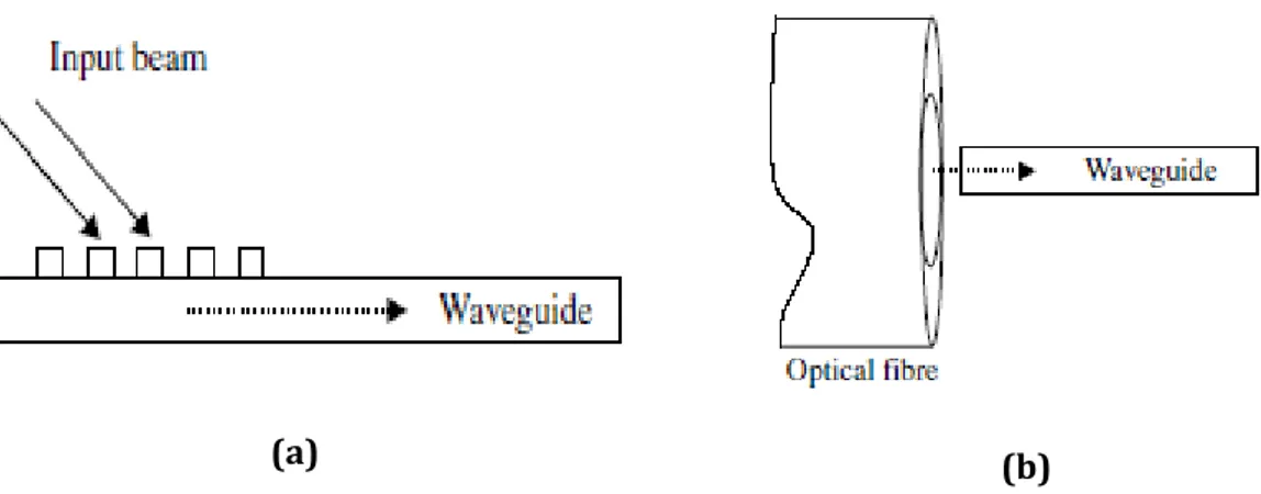
(a) (b)
Figure 2: Commonly used fiber to chip coupling techniques (a) Grating Coupling
(b) Edge Coupling [17]
One of the difference between grating and edge coupling is that the former one includes using straight or focused grating couplers whose geometry is such that they focus the Gaussian beam emitted by single mode optical fiber (SMF) lowering its mode field diameter (MFD) from 10.4 μm, obtained with a source of 1550 nm wavelength, to a value low enough to couple into sub-micrometre sized silicon waveguides, however this is not the case in latter technique, which usually consists of an inverse taper section that reduces the width of the waveguide progressively along the direction of propagation of light. Hence, in edge coupling technique, special kinds of optical fibers, like lens fiber or Ultra High Numerical Aperture (UHNA) fiber, are used which reduce the mode field diameter sufficient enough to enable efficient coupling. Lens fiber are single mode fibers with conical tips acquired by either polishing the facet or laser-ablating it into conical shape. The conical tip focuses the 10 μm MFD of the fiber core to a diameter of about 2-4 μm making edge coupling possible. However, lens fiber suffer from the disadvantage of being extremely delicate at the tip, a slight damage to the tip can render the lens fiber completely useless for edge coupling. Another disadvantage associated with lens fiber is that it is extremely challenging to align multiple lens fibers for multi-fiber coupling. Alternatively, using UHNA fiber can rid of these challenges. UHNA fibers have a much higher refractive index contrast as compared to SMF which results in fiber modes having MFD of around 3-4 μm thus offering a good modal overlap and coupling efficiency. Although UHNA fibers are expensive as compared to SMF, short pieces of UHNA fiber can be spliced with SMF having low splice loss and enabling efficient coupling at relatively lower cost. The coupling loss in edge coupling is dependent on various processes such as, fiber to tip mode mismatch, losses arising from mode conversion along the tapered waveguide, quality of chip facet and reflections at the chip facet [15]. The adiabatic reverse tapers require long taper for adiabatic conversion of the optical mode,
18
making it disadvantageous for integrated photonics, however different techniques to reduce this length can be found in literature [18].
The back-reflected spectrum from the FBG sensor, shown in figure 1, coupled into the interrogator can have both TE and TM polarizations, thus using grating couplers for sensor-interrogator interface can be problematic and inefficient although they provide fairly relaxed alignment tolerance as compared to edge couplers, which is an attractive feature in terms of packaging [19].
2.1.2.
Waveguides and Waveguide Modes
Waveguides are structures etched on the wafer that use a guiding mechanism, like total internal reflection or successive refocusing, to confine and guide electromagnetic wave parallel to its axis. Optical waveguides can be categorized based on various parameters such as material, refractive index distribution, geometry etc. and are broadly categorized as:
Planar Waveguides: The light is confined only perpendicular to the direction of propagation as the core is sandwiched between layers of cladding in x-direction only as shown in figure 2a. The index profile is denoted by n(x). Based on field distribution in the waveguide, two orthogonal modes of TE and TM can exist. When the electric field is transverse to the direction of propagation it is called TE mode. The TE mode for a waveguide such that light is confined in x direction, as shown in figure 3a, the fields are such that Ey = Ez = Hx = 0 while for the TM mode the fields will be such that Hy = Hz = Ex = 0.
Non-Planar Waveguides: The light is confined in two dimensions, x and y, because the core is confined by the cladding from all directions as shown in figure 3b. The index profile is denoted by n(x,y).
(a) (b)
Figure 3: Waveguides and optical confinement (a) Planar Waveguide (b) Non-planar waveguide [20]
19
Waveguide modes are electromagnetic waves travelling along a waveguide with a specific phase velocity, polarization, group velocity and cross-sectional intensity. The phase velocity that a mode travels with is given by
𝑝ℎ𝑎𝑠𝑒 𝑣𝑒𝑙𝑜𝑐𝑖𝑡𝑦 = 𝑐 𝑛𝑒𝑓𝑓
where c is speed of light in vacuum and neff is the effective refractive index of the mode.
The dimensions of the waveguide is one of the parameters that govern which modes will propagate through it. Most waveguides allow modes of two orthogonal polarizations, with one of the field components being dominant along the horizontal direction. As the waveguide dimensions increases the single mode regime changes into multimode. Each mode propagates the waveguide with propagation constant, β, given by
𝛽 = 𝑛𝑒𝑓𝑓
2𝜋 λ
where 𝜆 is the wavelength of light. Suppose the propagation constant of the orthogonal modes, TE and TM, are denoted with βTE and βTM respectively then after light has propagated
a distance x, the phase difference between the orthogonal modes, ∆φ, is given by ∆φ = |β𝑇𝐸− β𝑇𝑀| × 𝑥
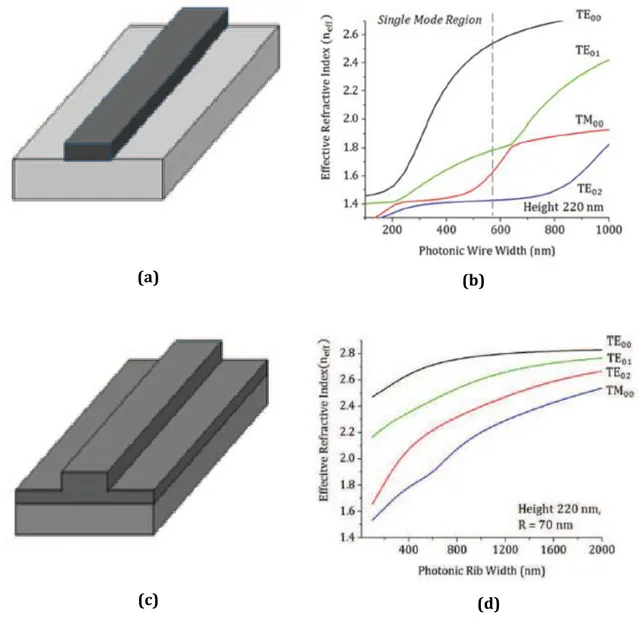
Generally, in PICs non-planar waveguides are used as they offer two-dimensional confinement of light. Based on the geometry of the waveguides there are many kinds of non-planar waveguides, such as buried waveguide, ridge waveguide, diffused waveguide, rib waveguide etc., have been used for device application in the optical industry. However, ridge waveguide and slab waveguide, shown in figure 4a and 4c respectively, are the only ones relevant to this thesis so their geometry will be briefly discussed. Ridge waveguides, also known as wire waveguides, based on SOI have silicon core and silica cladding. A mode is guided along the waveguide when its effective refractive index is smaller than the core and larger than the cladding. Ridge waveguides, shown in figure 4a, have a silicon core surrounded by silica-based cladding. Generally, the ridge waveguides are 220 nm high and 450 nm wide as these dimensions are ideal for single mode operation in ridge waveguides. Figure 4 b and d show neff of different modes as a function of waveguide width for a ridge and
rib waveguide, respectively. Single mode operation which is essential for many functional devices can be ensured by considering the graphs shown in figure 4 b and d while determining the dimension of the core of waveguide [20].
20
(a) (b)
(c) (d)
Figure 4: Non-planar waveguides and effective index of the modes propagating through them for
different widths (a) Ridge Waveguide (b) neff vs waveguide width for ridge (c) Rib Waveguide (d)
neff vs waveguide width for rib [20]
Different modes have different effective index and propagation constant, this results in birefringence, so the various polarization modes have a phase difference as they travel along the waveguide and are unable to couple together. Thus, creating a need for polarization diversity.
2.1.3.
Polarization management
In order to avoid the problem of polarization dependence in silicon photonic devices in general, without using polarization maintaining fiber (PMF), some sort of polarization diversity scheme needs to be adopted. Typically, polarization diversity was achieved by using different methods to split the orthogonal polarizations [21] which are then processed using separate circuits [22] and [23]. Another more efficient scheme consisting of polarization beam splitters and rotators is extensively used to attain polarization diversity. The two
21
orthogonal polarizations of the input beam to a polarization beam splitter are efficiently split and at the output we get the two polarizations, transverse electric (TE) and quasi-transverse magnetic (TM) as separate beams [24]. If the now separated TM beam is given as the input to the polarization beam rotator it will have its polarization rotated by 90ᵒ [25]. Using the method explained above it is possible to split the input beam’s polarizations before rotating one of them by 90ᵒ using a polarization splitter rotator (PSR) [14], conversely, it is also possible to rotate one of the polarizations before splitting them using a polarization rotator splitter (PRS) [26]. Using any of both approaches ultimately two signals with a particular polarization are obtained which can be guided through the rest of the optical circuit maintaining polarization diversity, thus, it can be said that both, PSR and PRS, are essentially the same in terms of functionality and both terms can be used interchangeably. PSRs are used in FBG interrogators to rotate all the TM polarization into TE essentially resulting in polarization independent interrogators. Different PSR designs currently under research will be discussed briefly in the next section.
2.2. State of Art of Integrated-optic FBG Interrogators
Recent advancements in photonic integration have paved new ways for development of compact, cost-effective and stable FBG interrogators, which will be able to address the demanding requirements of today’s market sectors.Several approaches of integrated FBG readout units based on the silica PLC, III-V group materials and SOI platform can be seen in literature, features of some of these approaches have been summarized in table 1. An FBG sensor interrogator operating on passive demodulation technique demonstrated in[27] is based on monolithic PLC technology with CMOS electronics. It operates using WDM filtering such that the Bragg wavelength shift is converted into linear variation in intensity, permitting the detection of peak wavelength position at the photodetector. The filtering is achieved using either a selective dispersive filter or an array waveguide grating (AWG) depending on the number of channels to be read with selective dispersive filter used for less than 12 channels and AWG used for more than 12 channels. The interrogator allows high speed dynamic integration but lacks in multiplexing abilities and integration of active function. In [28] FBG sensor readout unit based on generic InP PIC technology is demonstrated. InP platform is particularly interesting as it uniquely offers the possibility of monolithic integration of both active and passive components on a single semiconductor chip. In [28] the authors demonstrate two possible configurations for interrogators, first scheme exploits AWG along with multiple photodiodes and is used as a spectrometer, while the second scheme is based on tunable lasers. The
22
scheme based on AWG utilizing broadband source initially comprised of 12 channels with a channel spacing of 0.8 nm, but this design did not prove to be suited for FBG interrogation as it had channel spacing larger than the full width at half maximum (FWHM) of a typical FBG and low crosstalk between the AWG channels. An improved version of the design was implemented by increasing the number of channels to 36. High crosstalk between the channels is particularly helpful in detecting the back-reflected narrow-band spectrum of the FBG sensors. An off-chip polarization controlling solution was also proposed using a PBS and PM fiber. The second scheme comprised of tunable laser that provided a monochromatic signal and a single photodiode. Although this configuration is slow as compared to the first one because it requires sweeping of full wavelength range, it offers higher signal to noise ratio (SNR) due to higher spectral power density. An interrogation system based on SOI platform using micro-ring resonator (MRR) is demonstrated in [29]. In this configuration the MRR is used as tunable filter enabling interrogation of FBG sensors. A periodic signal is applied to the micro-heaters positioned on top of the MRR in order to exploit the thermo-optic effect in silicon. The shifts in Bragg wavelength can be found by tuning and detuning the MRR using the thermo-optic effect. The wavelength position of the FBG spectrum can be converted to a time domain signal using a periodic signal for the tuning of the MRR. Due to low intensity of back-reflected FBG sensor spectrum and filter selectivity, spectrum scanning methods based on tunable filters suffer from low SNR. Two digital signal smoothing techniques, moving average and Kaiser Filter were applied after the peak detection algorithm in order to reduce the aforementioned issue.
Technique Dynamic Range Frequency Sampling Output Power Optical Wavelength Resolution
WDM with dispersive filter or AWG [27] ≤10000 µɛ (1 FBG) ≤2500 µɛ (12 FBGs) 2 kHz (1 FBG) 20 kHz (5 FBGs) <5dBm ±5 pm @100 Hz Spectrometry: High crosstalk AWG [30][31] 4000 µɛ /4.8 nm (8 FBGs) 19.2 kHz External: 5 mW 5 pm Micro-ring resonator [29] 1600 µɛ (1 FBG) Static results only Unknown 49 pm Spectrometry: High crosstalk AWG/Hybrid integration [32] 5ᵒC and 80ᵒC (4 FBGs) 2 kHz 0.8 mW ±10 pm
Table 1: Comparison of various technologies used for integrated FBG readout units [27], [29],
[30], [31] and [32]
As the signal from the FBG sensor is typically narrow band and weak, it is extremely important to avoid any loss of the signal. The signal from FBG sensors can come in any
23
polarization so it is important to capture and analyse both polarization states of this. However, silicon photonic waveguides are strongly birefringent, therefore, in order to manage both polarizations simultaneously, a so-called polarization diversity scheme is needed. One common solution is to separate both polarizations, TE and TM into different waveguides, then rotate the TM to TE, and make two independent but identical TE circuits for the analysis of the signal. Usually, TE polarization is preferred in silicon photonics because of its better confinement of the light. This device is called Polarization Splitter-Rotator (PSR), and it is an important building block in silicon photonics. By using this device, if the polarization of the input light drifts, the relative powers in each subcircuit will vary, but the total power will be approximately the same and no power will be lost.
2.3. State of Art of Polarization Splitter Rotators
Recently, various techniques have been reported to make a PSR. These techniques can be broadly classified into two categories, mode evolution based PSR and mode coupling based PSR [33]. Many implementations of PSR based on mode evolution techniques using different structures such as tapers, multimode interference (MMI) structures, slanted waveguides and Y junctions can be found in literature [34], [35] and [36]. Similarly, there are many implementations of PSR based on mode coupling theory found in literature. The key technology used in such designs is based on asymmetrical directional couplers (ADC) [37]. The ADCs used can be designed by means of various structures of waveguides (slot/strip/rib), taper-etching, sub-wavelength grating and double-etched bends [38]. Symmetrical directional couplers based PSRs can be implemented easily owing to the simple design, however, PSRs based on symmetrical DCs will be of larger length due to weak birefringence [39]. There is also evidence in the literature of research being done on combination of mode evolution and mode coupling techniques for designing PSRs. Such PSR designs can be found in [26] where bi-level adiabatic taper is followed by an adiabatic directional coupler. The structure of the PSR design demonstrated in [26] is shown in figure 5a. As seen in figure 5b, the bi-level adiabatic taper converts the TM0 of input light into TE1 using mode evolution technique. The following adiabatic directional coupler uses mode coupling technique to couple TE1 mode from the broad waveguide into the narrower one which is then evolved into TE0 when the phase matching condition is met [40]. The use of adiabatic directional couplers in [26] for designing PSR has been demonstrated to be an efficient alternative to conventional asymmetrical directional couplers in terms of fabrication error tolerance [41].
24
Figure 5: (a) Schematic of the PRS. (b)Schematic depicting the profiles of mode 1 and mode 2 along the PRS[26]
One of the major challenges observed frequently for PSRs in SOI is that they often have requirements incompatible with common foundry processes. These requirements may include but not limited to extra layers, increased aspect ratio or an air cladding [14], [23], [24], [25], [42], [43], [44], [45], and [46]. The design proposed in [26] is the demonstration of PRS using bi-level taper for mode-conversion and it is based on common foundry processes reducing the aforementioned requirements. However, the major drawbacks of this design are that its total length is about 475 µm which is very long for a silicon-photonic building block, and the 90 nm partial etching of the bi-level adiabatic taper, which is not found in all foundries. One of the main objectives of the master’s project is to design an efficient PRS that has compact footprint as compared to the design proposed in [26] and fairly good performance. The proposed design will be based on 70 nm partial etching, which is very common in foundries, as it the etch depth that makes most efficient grating couplers.
The importance of polarization diversity in the field of high-speed optical communications and sensing cannot be emphasized enough. This is reason that for the past couple of decades, tremendous efforts are being put to perfect the design of PSRs to enable ease of fabrication, reduction in footprint and tolerance to fabrication errors along with high quality performance. The two techniques used for operation of PSRs have their own advantages and shortcomings. Mode coupling technique result in compact but wavelength and fabrication sensitive devices, whereas, mode evolution technique usually results in
25
devices tolerant to fabrication and having low insertion loss [46]. Currently, there are many different designs of PSR/PRSs found in literature, however, given the significance of these devices there is still need for more research to make further improvements in the currently available designs. In this section, a few of the existing PSR/PRS designs based on the two techniques and their combination will be discussed to weigh the pros and cons of the different designs.
PSRs based on tapered structures have gained a great deal of attention because they can lead to a fabrication tolerant compact device having high polarization extinction ratio (PER), one such design can be found in [34]. However, the taper-based transition unit of the PSR suffers from comparatively higher extra loss. The design proposed in [47] overcomes the issue of high extra losses seen in tapered structures by using slanted waveguides and also resulted in higher PER as compared to [34] but this device was disadvantageous in terms of size thus making it inappropriate for integration purposes. Other approaches based on mode evolution techniques involve using MMI structures, such devices are appealing in terms of high fabrication tolerance but given the length of MMI couplers and tapers, devices based on such structures have large footprint [47]. A PSR design based on Y-junction has been proposed in [36] which has the attractive features of low loss, broad bandwidth and compact footprint of 95µm. The aforementioned structures are based on mode evolution principle and such devices are usually fabrication tolerant, have a broad bandwidth and lower losses but suffer in terms of size because they rely on adiabatic transitions. On the contrary, devices based on mode coupling technique use the phase matching principle and PSRs made from such structures are usually compact in size but are sensitive in terms of fabrication and wavelength [48].
ADCs are one of the most commonly used structures for designing PSRs based on mode coupling techniques, although PSRs can be designed using symmetric directional couplers too but such PSRs are larger in size. Various PSR designs based on ADCs formed using different structures can be found in literature. PSRs formed by strip, rib and slot waveguide-based ADCs are found to be compact and efficient but such PSRs are either intolerant to minor fabrication errors or suffer from coupling losses between the waveguides [49]. An efficient PSR having robust fabrication tolerance can be designed using slanted silicon waveguides-based ADCs instead of strip and slot waveguides. Due to the slanting waveguides, the coupling is enhanced, and field concentration is comparatively decreased, thus, coupling length reduces and the fabrication tolerance enhances. This PSR design based on slanted waveguides was found to have high PER and low losses but the drawback of the slanted
26
waveguides is that they require specific processes which complicate the overall fabrication process [37]. A compact PSR can be formed by using sub-wavelength grating based ADC as presented in [50]. Although, the width of the waveguides used in this design are fabrication tolerant, the duty cycle of the gratings is fabrication sensitive [37]. The PSR designs in [51] are compact and fabrication tolerant but it was discovered that etched ADCs, double-etched bending-ADCs and taper-double-etched ADCs suffer from difficult and expensive fabrication process.
Few designs of PSRs using both mode evolution and mode coupling have also been reported [26] and [48] in an attempt to design an efficient PSR having a low crosstalk in common foundries but both these designs suffer from large footprint.
27
3 Design
The master thesis was aimed at contributing towards the goal of creating integrated FBG interrogators. In this regard, the importance of polarization diversity cannot be neglected. PSR play a vital role in avoiding unnecessary loss of signal from the FBG sensors to the interrogator due to polarization sensitivity of the interrogator. The master thesis was twofold with the first task involved in the thesis was designing an efficient PRS based on mode evolution technique. The PSR was designed by cascading a splitter with a rotator followed by a mode converter.
3.1. Introduction to Lumerical
All the devices were simulated using Lumerical suite, which is a high-performance software used to design, simulate and analyze different photonic components and systems. Lumerical suite has various IDEs shown in figure 6. Finite Difference Time Domain tool (FDTD) was used in order to design the devices. FDTD is a 3D electromagnetic simulator that uses time domain method, so the electric and magnetic fields are calculated as a function of time with the geometry of the structures defined in the x, y and z axis. As FDTD analyzes results of 3D structures, the simulations are time and memory consuming. The main motivation behind using FDTD rather than MODE was to use Particle Swarm Optimization (PSO) for the optimization purposes. Although varFDTD tool of MODE IDE uses the same solver physics as FDTD, it makes some approximations which collapse the 3D geometry of the devices into 2D essentially making the simulations less time and memory consuming, thus the usual approach is to design and optimize the device initially using varFDTD and then at the end do the verification of the simulated device using FDTD. However, the assumptions made by varFDTD make it unsuitable for devices having vertical asymmetry, so it is not an appropriate tool for simulating splitters and rotators. Given the mentioned reasons we opted to use FDTD tool for our designs despite the fact that its simulations are more time and memory consuming as compared to MODE.
28
Figure 6: Tools offered by Lumerical Suite
After the designing and simulation of the individual splitter and rotator, they were integrated into a PSR using INTERCONNECT of the SYSTEM suite. Interconnect is used for PIC simulations in both time and frequency domain.
3.2. TE0 and TM0 Splitter
The TE0 and TM0 splitter was designed using adiabatic directional coupler similar to design used in [52]. Adiabatic directional couplers are directional couplers in which the geometry of the waveguides gradually change along the coupling region. By doing so, the performance becomes more robust to fabrication deviations than standard directional couplers. The design was optimized to make a shorter device suitable for efficient splitting of both modes for a broadband source of range 1510 nm to 1590 nm.
3.2.1.
Lumerical Settings
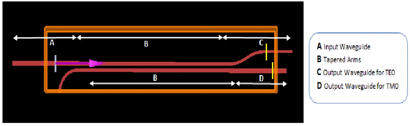
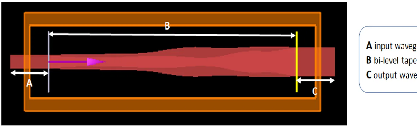
The xy view of the designed splitter can be seen in figure 7. The overall splitter is of 41.9167 µm length. The splitter was designed by first defining the tapers and then attaching the bends, input and output waveguides. The source is injected from the left of the top arm of the tapered directional coupler. The majority of TM0 fields then couple into the bottom arm while the majority of TE0 fields is transmitted through the top arm of the coupler. The width of the tapered section of the top arm reduces along the output of directional coupler and vice versa for the bottom arm.
29
Figure 7: TM0 and TE0 Splitter
As we want to simulate the device over a range of wavelengths, hence the wavelength dependence of refractive index of silicon should be taken into account in order to ensure correct description of dispersion effects. Considering this reason, the Si Palik material available in the Lumerical materials library is not sufficient, hence, a Lorentz model material named ‘Si Dispersive&Lossless’ was used for the waveguides used to design the adiabatic directional coupler. Wavelength dependent refractive index in the Lorentz model can be found by following equation
𝑛2(𝜆) = 𝜖 + 𝜖𝐿𝑜𝑟𝑒𝑛𝑡𝑧𝜔0
2
𝜔02−2𝑖𝛿0𝜆2𝜋𝑐− (2𝜋𝑐𝜆 )2
where ϵ denotes permittivity, ϵLorentz denotes Lorentz permittivity and ω0 denotes Lorentz
resonance.
This model fulfils the Kramers-Kronig relations making it compatible with FDTD. The coefficients used in the simulations performed are shown in figure 8, and they are optimized to fit experimental data over the wavelength range of 1.15 to 1.8 µm to simulate a dispersive and lossless Si material [53].
30
Figure 8:Coefficients of Si Dispersive&Lossless material
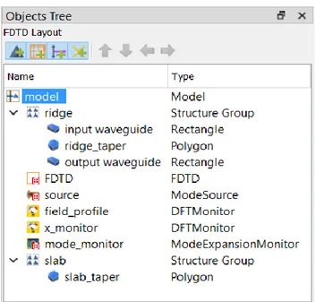
Generating the geometry of the adiabatic coupler, using educated guesses for different parameters discussed further, was followed by defining the FDTD simulation region and placement of source and monitors. Figure 9 shows the objects created under model for the designed splitter. The structure groups ‘linear_taper’ and ‘linear_taper2’ contained rectangular waveguides for the output arm of TM0 named ‘cross’ and input arm respectively along with ‘solid’ structures for the two tapered arms of the adiabatic coupler, denoted by A, B and D in figure 7. The ‘inS’ structure group was used to define the bend of the bottom arm of the coupler using a ring waveguide with a radius of 3 µm. This arm was terminated on the other end with a rectangular waveguide of 10 µm named cross in figure 10. Apart from the input and tapered section the top arm was formed with Structure group ‘outS’ consisting of two ring waveguides of radii 6 µm cascaded to form the bend followed by a rectangular waveguide ‘out_x’ of length 5 µm to create the output arm for the TE0, denoted by C in figure 7.
31
Figure 9: Object Tree of TE0 and TM0 splitter
While setting the FDTD simulation region, the background index was set to 1.444 to simulate silicon dioxide in the simulation region apart from the waveguide structures, this removes the need to define substrate and top cladding. For initial simulations, the mesh accuracy was set to 3 which corresponds to 14 points per wavelength providing a good trade-off between accuracy, simulation time and memory requirements.
In the simulations performed, “Mode” type source was used to enable selection of particular mode propagation at the input of the directional coupler. The wavelength of the source was set in the ‘Frequency/Wavelength’ tab from 1510 nm to 1590 nm to analyze the results of the device over a broad band. Figure 10a shows the general settings of the source and the pink arrow in figure 7 denotes the source. Selecting “user select” for the mode selection we can select the mode according to our requirement and also confirm the decay of fields by visualizing the log scale plots as shown in figure 10 b. The dimensions of the simulation region, source and monitors were set such that the fields in the log scale plots along y and z axis decay at least up to 10-4 ensuring that
32
(a) (b)
Figure 10: (a) General Properties of Source (b) Source field decay in log scale As the splitters and rotators require working with specific polarizations and waveguide modes so for these devices 2 kinds of monitors were used simultaneously:
Frequency-domain field and power monitor: It gathers the field profile in frequency domain by taking Fourier transform of the fields in time domain through some spatial regions of the FDTD. These monitors can be 1D or 2D, if the structure being simulated is 3D, as in the case of the rotator 2D monitors are to be used.
Mode expansion monitor: It is used to analyze how much power is transmitted into the modes of interest. These monitors make use of overlap analysis to compute the propagating components of the mode of interest, from the frequency-domain field and power monitor, at any point in the simulation region. Given that the supported mode profile is a function of wavelength so for broadband simulations the number of frequency points should be set to a value greater than 1 in the settings for this monitor. The mode expansion monitor type does not monitor simulation results, but it rather takes the field data measured by the frequency-domain field monitor defined in its setting and overlaps that data onto the modes of interest. [53]
As seen in figure 9, three frequency-domain field and power monitors; E-propagation, TE_xmon and TM_xmon, were used in the splitter design. ‘E-propagation’ monitor was added to see the electric field of the modes while light travels along the adiabatic coupler’s length thus the
33
monitor type was set to 2D Z normal. The ‘TE_xmon’ and ‘TM_xmon’ were put at the outputs of top and bottom arms of the adiabatic coupler respectively, to visualize the transmission over the wavelength range 1510-1590 nm so the monitor type was set to 2D X normal. The transmission measured by the TE_xmon and TM_xmon monitors was then used by the TE_mode_mon and TM_mode_mon respectively to measure the transmission of modes of interest. Care was taken to center both kinds of monitors around the same position relative to the arms of the adiabatic coupler because the overlap analysis of the field and desired modes is done relative to the center point of both monitor types. Figure 11 shows the settings for the TE_mode_mon, similar settings were used for the TM_mode_mon with the exception of selecting TM_xmon in the ‘Monitors for expansion’ tab.
Figure 11: Settings of Mode Expansion monitors
TM polarization has shorter coupling length so the parameters for which TM is managed to couple, a strong TE can be found in the other arm of the coupler so while optimizing the splitter the transmission of the TM was observed. The adiabatic directional coupler was designed such that the width of the tapered section of the top arm reduces along the length and vice versa for the bottom arm as seen in figure 8. Initially the width of the wider ends, w1, and widths of the narrower ends, w2, were set as 590 nm and 410 nm respectively separated by a gap of 400 nm, these initial values were taken by analysing deigns of adiabatic couplers in [52]. Keeping these parameters, the length of the taper was swept from 15 µm to 25 µm as shown in figure 12a. In the graph of transmission versus length, the maximum transmission was observed at 20.6667 µm which was taken as the length of the adiabatic tapers of the directional coupler’s arms. To reduce
34
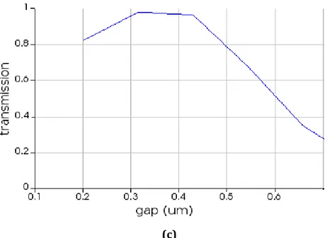
the complexity, the width of the wider ends of the arms, w1, were fixed to 590 nm and the width of the narrower side was swept from 390 nm to 500nm to find the optimum width as shown in figure 12b. In the graph of transmission versus the width of taper, the highest transmission was found for a width of 455.556 nm so w2 was set to 455.556 nm. Next, the gap between the adiabatic tapers was optimized by sweeping it from 200 nm to 700 nm as shown in figure 12c. Observing the graph of transmission versus gap a gap of 314.286 nm was selected.
(a)
35
(c)
Figure 12: Sweep results (a) Transmission vs length of adiabatic tapers of the coupler's
arms (b) Transmission vs width of narrow end of taper (c) Transmission vs gap
3.2.2.
Results and Analysis
In this section the results obtained from simulating the adiabatic directional coupler performing as a splitter will be discussed.
3.2.2.1. Field Profile
The field profile diagrams shown in figure 13 a and b show clear splitting of the fundamental TE and TM polarization into the TE and TM ports respectively. The strong fields in the appropriate arm for a particular input polarization and very weak fields in the cross arms shows that the splitter is working efficiently.
(a)
(b)
Figure 13: Electric fields of light propagating through the splitter (a) Electric field for TE
36
3.2.2.2. Transmission
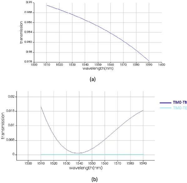
The performance of the splitter was also measured by observing the transmission of the wanted and unwanted polarizations at each output port by injecting the fundamental TE and TM polarized light in the structure. The transmission of desired and undesired polarizations at TE port can be seen in figure 14 a and b respectively. As seen in figure 14a, the transmission of TE polarization at its relevant port was measured having a range of 97.82-98.95% with a transmission of 97.82% at 1550 nm. Out of the unwanted polarizations in TE output port shown in figure 14b, the maximum transmission was observed for TM0 polarization at 1510 nm having a value of 1.6%, for the same polarization a weak transmission of 0.2% is observed at 1550 nm. The weak TM0 polarization is the remnant of the TM polarization that was not coupled in the TM port. From figure 14b we can state that the coupling of unwanted polarizations in the TE port is very weak.
(a)
(b)
Figure 14: Transmission at TE output port of splitter (a) transmission of wanted signal (b) transmission of unwanted signal
37
Figure 15 a and b show the wanted and unwanted signal at the TM output port. As the splitter is made by an adiabatic directional coupler so the all the TM0 signal apart from the remnant signal seen in figure 14b is coupled into the TM output arm as the desired signal with transmission ranging from 98.15-99.94%. Similarly, the TE0 leaked into the cross arm appears as an undesired signal in the TM output port with a maximum transmission of 1.6% at 1590 nm, as shown in figure 15b. Comparing the graphs for transmission of at the TE and TM output port we notice that for this particular length of the coupler more TE power transfers into the cross arm as compared to TM. However, these leakages of powers are relatively low and can be further minimized by cascading a couple of splitters at the input of the rotator.
(a)
(b)
Figure 15: Transmission at TM output port of splitter (a) transmission of wanted signal (b)
38
3.2.2.3. Fabrication Tolerance
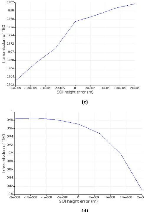
The robustness of the splitter was checked in the simulations to determine how robust it is to fabrication errors. The simulations were performed to check the effect of changes in widths of the arms of adiabatic directional couplers arms, shown in figure 16 a and b, and the effect of changes on the SOI height of the wafer on both polarizations, shown in figure 16 c and d. The simulations were performed for a variation of ±20 nm for seven data points in each case. Comparing curves in figure 16 a and b, we notice that the TM polarization was affected by the change in widths more than TE polarization. The reason for this is associated with the working of the adiabatic directional coupler as a splitter, TM polarization has shorter coupling length as compared to TE polarization so it is affected by changes in the structure of the splitter more than TE polarization. However, for both polarizations the transmission is affected less than 3%, with increase in transmission for both polarizations when the arms of the splitter get wider than the design. The low effect of changes in widths show that the splitter is tolerant to fabrication errors.
Evaluating graphs in figure 16 c and d, it is again noticed that TM polarization is affected more that TE by the changes in the SOI height. The changes in SOI height results in ±1% change in the transmission in TE polarization whereas for TM polarization transmission drops by 16% with an increase in SOI height by 20 nm. This much more drastic effect on the transmission of TM polarization as compared to TE polarization is associated with the orientation of the electric field in these polarizations; electric field in TM is vertical while in TE it is horizontal making TM more susceptible to changes in SOI height. The graphs in figure 16 a-d should have maximum transmission at no error because the splitter design was optimized, however this is not the case, most likely because the limited number of points used in the optimization did not strictly provide the absolute maximum in transmission for the nominal geometry.
39
(a)
40
(c)
(d)
Figure 16: Robustness of the splitter (a) transmission of TE vs error in width of splitters arms (b)
transmission of TM vs error in width of splitters arms (c) transmission of TE vs error in SOI height
(d) transmission of TM vs error in SOI height
3.3. TM0 to TE1 Rotator
Polarization rotation can be achieved in vertically asymmetric structures as the optical axis in such structures can be tilted due to the asymmetry. Vertical asymmetry generates coupling between different polarization states resulting in polarization rotation. However, rotation can only occur between modes having the same electric field parity, for instance TM0 and TE1. This
41
means that the generated TE mode is not the fundamental, but the second mode, so it requires a subsequent mode converter. In order to achieve cross-coupling between TM0 and TE1 modes, vertical symmetry needs to be broken, which can be achieved in many different ways, like using an air cladding instead of silica cladding or using a rib waveguide. Using the air cladding has disadvantages including sensitivity of the sample to the environment and it is also not commonly available in all foundries. The easiest way to break the vertical symmetry is using rib waveguide and that is the approach used in this thesis, as in [54].
The design of a TM0 to TE1 rotator was based on [54] but in order to make the design compatible with the common etching depth of 70 nm provided by most foundries for grating couplers, the slab of the bi-level taper was heighted at 150 nm rather than the 90 nm in [54].
3.3.1.
Lumerical Settings
Figure 17 shows the xy view of the designed rotator as seen in FDTD. The length of input and output waveguides were set to 2 µm while the ridge and slab of the bi-level taper were 13 µm in length. The section B of figure 17 is the bi-level taper, the input and output denoted by A and C respectively are straight waveguides of height 220 nm added at the start and end of the bi-level taper in order to ensure smooth transitions of the modes to and from the bi-level taper.
Figure 17: TM0 to TE1 rotator
The ‘Si Dispersive&Lossless’ material defined in figure 8 was used for bilevel taper, input and output waveguides to take into account the dependence of refractive index over wavelength. The bi-level taper was simulated by defining 11 different widths denoted by w0 through w10, for both the ridge and slab. Considering that TM0 mode will enter the bi-level taper, the width of the input waveguide and w0 for ridge and slab is set to 480 nm. As the bi-level taper is expected to rotate a vertical polarization into horizontal polarization, so an educated guess, denoted in table 2, is made for values of the widths w1 to w9 with an increasing trend of widths towards the output of the bi-level taper. The terminating width, w10, of the ridge and slab of the bi-level taper is set to 1250 nm, width of the following output waveguide is also set to the same value. The value of
42
terminating width is chosen keeping in mind that a higher order mode of TE1 will be exiting the bi-level taper.
After defining the dimensions of input, output waveguides and bi-level taper, the FDTD simulation region was set, which was followed by placing the source and monitors. The objects created in the TM0 to TE1 rotator are shown in figure 18
Figure 18: Object tree of TM0 to TE1 rotator
Similar to the splitter the background index and mesh accuracy was set to 1.444 and 3 respectively in the settings of the FDTD simulation. The boundary conditions were set to metal in z direction while optimizing the structure while using PML in x and y direction. PML boundaries absorb all the incident light avoiding back reflections, whereas metal boundaries operate in opposite manner by behaving as mirrors and reflecting all the incident light. However, metal boundary is the fastest in simulations so using metal along z axis speeds up the simulations which is preferred during the initial calculations and optimization process. After the completion of the optimization process, the mesh and boundary settings were changed to increase the accuracy of the simulation results.
The ‘Mode Source’ was used to enable selecting the desired mode, in this case TM0. As evident from figure 18, the rotator design included two frequency-domain fields; the monitor type for the first monitor named field_profile was set to 2D Z normal to get a view of the field profile as it travels in the xy plane through the rotator, while the second monitor named x_monitor was set at the output of the bi-level taper to visualize the transmission at the output. The monitor named mode_monitor was the mode expansion monitor used in the rotator design to observe the polarization conversion from TM0 mode to TE1 at the output of the bi-level taper so the TE1 mode was selected. The number of frequency points for the mode_monitor was set to 3 since the modal
![Figure 3: Waveguides and optical confinement (a) Planar Waveguide (b) Non- Non-planar waveguide [20]](https://thumb-eu.123doks.com/thumbv2/123dokorg/2926409.18634/18.892.185.764.852.1080/figure-waveguides-optical-confinement-planar-waveguide-planar-waveguide.webp)
![Table 1: Comparison of various technologies used for integrated FBG readout units [27], [29],](https://thumb-eu.123doks.com/thumbv2/123dokorg/2926409.18634/22.892.106.814.748.1032/table-comparison-various-technologies-used-integrated-readout-units.webp)