in deep submicron technologies
Dipartimento di Ingegneria dell’Informazione, Elettronica e Telecomuni-cazioni
Dottorato di Ricerca in Ingegneria Elettronica – XXVII Ciclo
Candidate
Simone Bongiovanni ID number 798246
Thesis Advisor
Prof. Alessandro Trifiletti
Co-Advisor
Prof. Giuseppe Scotti
A thesis submitted in partial fulfillment of the requirements for the degree of Doctor of Philosophy in Electrical Engineering 2nd March 2015
Prof. Giovanni Busatto - Università di Cassino
Prof. Gian Carlo Cardarilli - Università di Roma Tor Vergata Prof. Luigi Zeni - Seconda Università degli Studi di Napoli
Design techniques for secure cryptographic circuits in deep submicron technolo-gies
Ph.D. thesis. Sapienza – University of Rome ISBN: 000000000-0
© 2015 Simone Bongiovanni. All rights reserved
List of Figures
1.1 A schematic representation of the different possible methodologies to
design digital VLSI circuits. . . 3
1.2 Block diagram of a standard digital design flow [119]. . . 6
1.3 Description of a standard side-channel scenario [116]. . . 10
1.4 Origin of the dynamic currents in a CMOS inverter when output switches from low to high (left) and from high to low (right). . . 14
1.5 Origin of the leakage currents in a CMOS inverter when input is low (left) and high (right) in steady state condition. . . 14
1.6 Block diagram describing the complete PAAs procedure [72]. . . 20
1.7 A list of 24 block ciphers adoptable for lightweight applications. . . . 25
1.8 Different elaboration steps of the encoding procedure of AES-128. . . 27
1.9 S-Box of the SubstitutionBytes layer of the AES encoder. . . . 28
1.10 Different elaboration steps of the encoding procedure of Serpent. . . 29
1.11 S-Boxes of the Serpent encoder. . . 30
1.12 Different elaboration steps of the encoding procedure of PRESENT. 31 1.13 S-Box of the PRESENT encoder. . . 31
1.14 A model of the contribution of the load capacitance [124]. . . 39
1.15 Performances and features of some selected DPLs styles. . . 41
1.16 A detailed description of a standard semi-custom design flow. . . 42
1.17 A detailed description of a secure semi-custom design flow for imple-menting a DPL circuit. . . 43
2.1 Two possible realistic scenarios for practical PAAs: an attacker can measure filtered (a) or non-filtered current traces (b). . . 48
2.2 Timing diagram of logic-0 (a), logic-1 (b) signal in RTZ logics . . . . 52
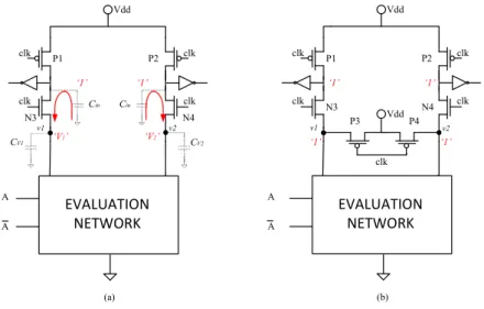
2.3 Timing diagram of logic-0 (a), logic-1 (b), invalid (c) signal in TELs 53 2.4 Cell template of a TEL gate composed of two independent circuit halves implementing the logic functions F1 and F2. . . 55
2.5 Cell templates of basic combinational gates, compatible with the TEL encoding and designed with only AND logic gates. . . 56
2.6 Full custom cell template of a TEL-compatible inverter (iDDPL style) (left) and a RTZ inverter (SABL style) (right). . . 56
2.7 A pipelined circuit template in which the information is enclosed inside a time interval δ . . . . 60
2.8 Variation of the delay δ along combinational logics before and after a register. . . 62
2.9 Testbench for the simulations of the TEL inverter cell with an
unbal-anced load and a variable RC filter on the PSN. . . 63
2.10 Distribution of the current samples during the evaluation phase for the unbalanced TEL inverter, with a variable filtering capacitance. . 63
2.11 PAAs scenario for a TEL circuit, with the insertion of an on-chip filter for removing the high frequencies components directly at layout level. . . 65
2.12 ∆F F T vector for the TEL inverter for different value of the mismatch factor (δ = 500ps): MF = 1 (black), 2(red), 3 (green) and 4 (blue). . 68
2.13 ∆F F T vector for the SABL inverter for different value of the mis-match factor: MF = 1 (black), 2(red), 3 (green) and 4 (blue). . . 68
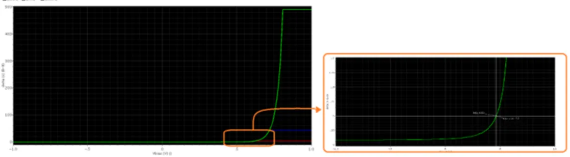
2.14 Plot of the frequency f0 as a function of δ. . . . 71
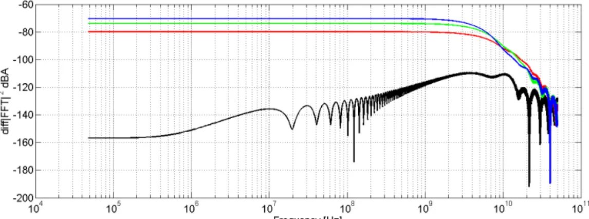
2.15 ∆F F T vector for the TEL inverter for δ = 100ps . . . 71
2.16 ∆F F T vector for the TEL inverter for δ = 5ns . . . . 71
2.17 A generic bit slice hardware implementation of the Serpent encryption processor. . . 74
2.18 Data path of the SERPENT-block using a DPL implementation. . . 74
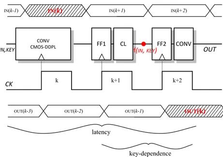
2.19 Timing diagram of in/out signals and latency of the processed words at each clock cycle of the pipeline. . . 75
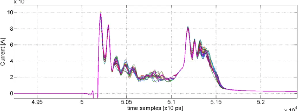
2.20 Current traces for each of the 256 input combinations of the TEL circuit in the evaluation and postcharge phases of the third clock cycle. 77 2.21 FED vector for TEL circuit with low unbalance on the interconnect wires (black curve) and with a maximum unbalance (M F = 3) (red curve). . . 77
2.22 Equivalent circuit model for the testbench in Cadence simulations [59] 78 2.23 FED vector for the TEL circuit calculated after having filtered the current traces (f0 = 30M Hz). . . . 78
2.24 Correlation coefficients plot of the 256 simulated traces of the TEL circuits as a function of time; correct key is indicated in bold black line. 80 2.25 Correlation coefficients plot of the 256 simulated traces of the SABL circuits as a function of time; correct key is indicated in bold black line. 80 2.26 PBC of the TEL circuit for the bits of the word at the output of the S-Box (correct key in bold). . . 82
2.27 PBC of the SABL circuit for the bits of the word at the output of the S-Box (correct key in bold). . . 82
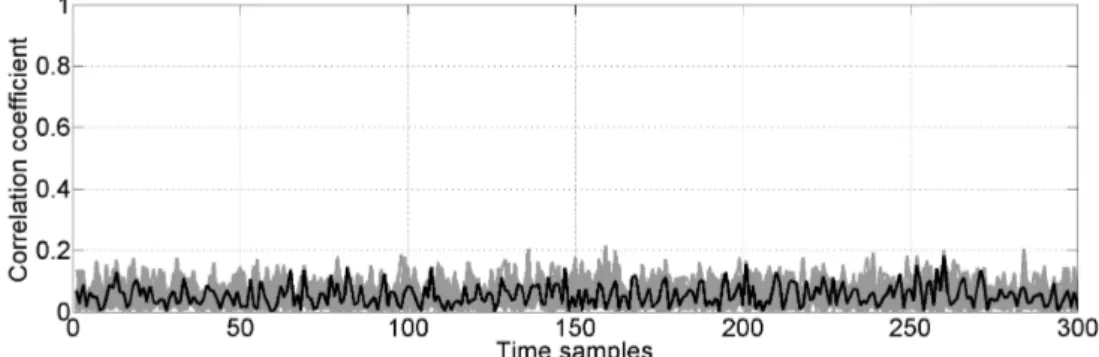
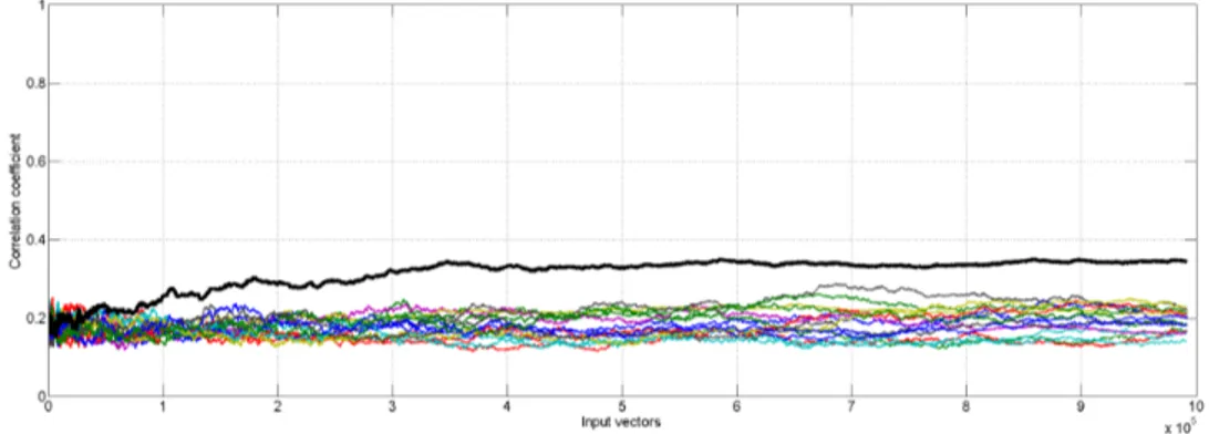
2.28 Correlation coefficients plot as a function of the number of input plaintexts for the TEL circuit, in the case of σnoise≈ 2 · 10−4; correct key is indicated in bold black line. . . 84
2.29 Correlation coefficients plot as a function of time for the TEL circuit in the case of σnoise≈ 2 · 10−4; correct key is indicated in bold black line. . . 84
2.30 Correlation coefficients plot as a function of time for the SABL circuit in the case of σnoise≈ 2 · 10−4; correct key is indicated in bold black line. . . 86
2.31 Correlation coefficients plot as a function of time for the SABL circuit in the case of σnoise≈ 2 · 10−4; correct key is indicated in bold black line. . . 86
2.32 MTD as a function of the noise standard deviation. . . 86 2.33 Correlation coefficients plot as a function of the number of input
plaintexts for the TEL circuit, in the case of σnoise ≈ 10−3< σCRnoise;
correct key is indicated in bold black line. . . 87 2.34 Correlation coefficients plot as a function of time for the TEL circuit
in the case of σnoise ≈ 10−3 < σCR
noise; correct key is indicated in bold
black line. . . 87
3.1 Cell template of an iDDPL BUFF/INV gate for the TEL circuits. . 92 3.2 Timing diagram of the BUFF/INV cell in correspondence of signal
(1,0) (logic-1 in CMOS domain) . . . 92 3.3 iDDPL gate suffering on the memory effect (a) and iDDPL gate
without memory effect with the presence of internal keeper transistors (b) . . . 93 3.4 Cell template of an iDDPL AND/NAND logic gate. . . 95 3.5 Current traces of an iDDPL BUFF/INV (left) and an AND/NAND
gate (right) . . . 95 3.6 Circuit for the conversion of a CMOS signal into the TEL domain for
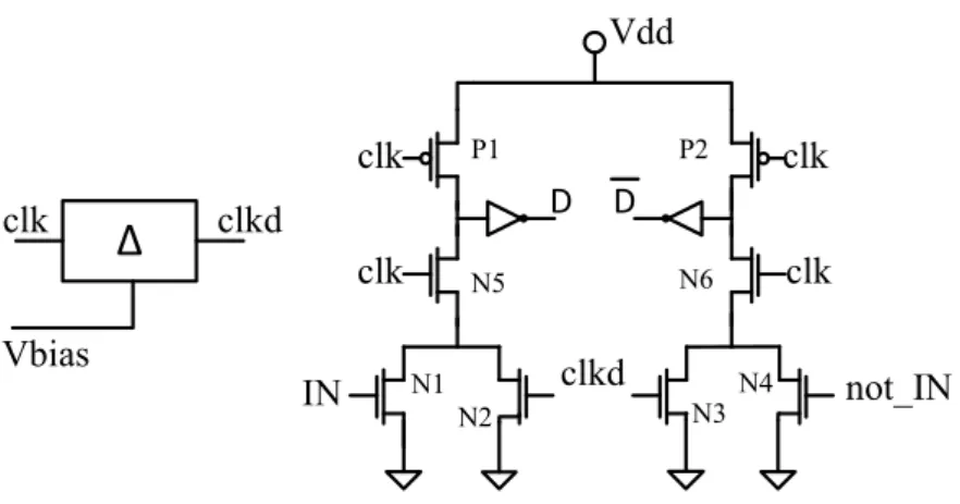
the iDDPL style. . . 95 3.7 Implementation of a delay element line based on a current starved
inverter for the DDPL flip-flop. . . 96 3.8 Dependence of the delay δ with the control voltage Vbias . . . 97 3.9 A basic iDDPL AND/NAND gate with the equivalent circuits of the
evaluation network. . . 102 3.10 Time diagram of the evaluated signals at the output of a basic DDPL
AND/NAND cell for all possible inputs. . . 103 3.11 A basic iDDPL AND/NAND gate with the equivalent circuits of the
evaluation network. . . 104 3.12 Time diagram of the evaluated signals at the output of the improved
iDDPL AND/NAND cell for all possible inputs, when t2 > τ1. . . 105
3.13 Time diagram of the evaluated signals at the output of the improved iDDPL AND/NAND cell for all possible inputs, when t2 < τ1. . . 105
3.14 A basic DDPL XOR/NXOR gate with the equivalent circuits of the evaluation network. . . 107 3.15 Time diagram of the evaluated signals at the output of a basic DDPL
XOR/NXOR cell for each input, for the case t2 > τ1. . . 107
3.16 Time diagram of the evaluated signals at the output of a basic DDPL XOR/NXOR cell for each input, for the case t2 < τ1. . . 107
3.17 Early evaluation free iDDPL AND/NAND (left), OR/NOR (middle) and XOR/NXOR gate (right) with minimum number of transistors. 108 3.18 Logic gates implementation of balanced iDDPL multiplexer (left) and
full adder (right). . . 108 3.19 Waveforms of the differential signals at the output of a BUFF/INV
gate for different MF (up) and current peaks in evaluation/postcharge (down). . . 109 3.20 Distribution of the output delay δ for the combinational gates after
3.21 Superimposition of current traces for a basic (a) and an optimized (b) AND/NAND gate. . . 115 3.22 A combinational multi-level logic with 5 cascaded AND/NAND gates. 115 3.23 Superimposition of current traces for the multi level logic implemented
with basic (a) and optimized (b) AND/NAND gates. . . 115 3.24 Superimposition of filtered current traces for the multi level logic
implemented with basic (a) and optimized (b) AND/NAND gates. . 115 3.25 Block scheme of the iDDPL master-slave flip-flop. . . 118 3.26 Timing diagram of the signal processed in the DDPL master-slave
flip-flop. . . 118 3.27 Scheme of the input converter (left) and working principle (right). . 120 3.28 Timing diagram of the signals elaborated by the input converter. . . 120 3.29 Scheme of the differential CMOS XOR gate which controls the
trans-mission gates of the input converter. . . 120 3.30 A p-type master latch and working principle of a differential half circuit.121 3.31 Timing diagram of the signals elaborated by the master latch. . . 121 3.32 A n-type slave latch and working principle of a differential half circuit.123 3.33 Timing diagram of the signals elaborated by the slave latch. . . 123 3.34 Scheme of the improved input converter. . . 123 3.35 Superimposition of current traces for all possible input data in a
CMOS (a), WDDL (b), SABL (c), TDPL (d), DDPL (e), and iDDPL (f) 4-bit register (MF = 3). . . 124 3.36 Coefficient of variation (CV) for a CMOS (a), WDDL (b), SABL (c),
TDPL (d), DDPL (e), and iDDPL (f) 4-bit register as a function of the time samples in a clock cycle under different mismatch factors. . 125 3.37 Screenshot of the Coefficient of Variation for the master-slave iDDPL
4-bit register around the delay time δ under different mismatch factors.126 3.38 A comparison of the distribution of the average current for 100 clock
cycles for the DPL flip-flops under test (MF = 3). . . 126 3.39 Variation of the delay δ along combinational logics. . . 129 3.40 Timing of the signals at the input/output of a generic combinational
path. . . 131 3.41 Modelization of the routing of two standard cells: the differential
wires in red must be low-leakage. . . 136 3.42 Layout of some combinational iDDPL cells: BUFF/INV (a), AND/NAND
(b), OR/NOR (c), and XOR/NXOR (d). . . 136 3.43 Screenshot of the SERPENT-block after placement, with highlighted
the differential interconnect wires between two iDDPL cells. . . 136 3.44 Symmetric layout of the iDDPL master-slave flip-flop. . . 138 3.45 A detailed description of a secure semi-custom design flow to
imple-ment a TEL circuit using iDDPL gates. . . 140
4.1 Macro-blocks composing the SERPAES chip: the AES-block and the SERPENT-block . . . 142 4.2 Data path of a DPL-featured 4-bit unit implementing the first round
4.3 Schematic view of the S-Box S0 from Serpent algorithm implemented only with combinational CMOS gates; the critical path is also
indi-cated in figure. . . 144
4.4 Clock tree of the iDDPL core. . . 147
4.5 Deviation of the clock signals at the output of the buffers (pre-layout).147 4.6 Polarization circuit to generate the static voltage Vbias in the iDDPL core. . . 150
4.7 Dependence of the delay δ with the control voltage Vbias, for VDD= 1.2V .150 4.8 Waveforms of the input/output, clock and test signals of the iDDPL circuit before layout. . . 152
4.9 Variation of the tuning range curve for the different corners of the circuit. . . 154
4.10 Layout of the iDDPL core of the SERPENT-block. . . 157
4.11 Mismatch factor for the differential nets of the S-Box block of the iDDPL circuit: combinational gates (blue) and of flip-flops (red) output wires. . . 157
4.12 Waveforms of the input/output, clock and test signals of the iDDPL circuit after layout. . . 160
4.13 Deviation of the clock signals of the circuit due to the clock skew after layout. . . 161
4.14 Distribution of the value of δ on each differential combinational net of the iDDPL implementation of the S-Box for every input data. . . 161
4.15 Waveform of Vbias signal after post-layout simulations. . . 161
4.16 Layout of the SABL core of the SERPENT-block. . . 163
4.17 Complete layout of the SERPENT-block. . . 163
4.18 General architecture of the SERPENT-block. . . 164
4.19 LEF file of the SERPENT-block (screenshot). . . 165
4.20 Simplified schematic diagram of the AES-block of the SERPAES chip. 167 4.21 Block diagram and clock signal of the basic AES encryption unit (AES-0). . . 168
4.22 Block diagram and synchronization signals of AES-1. . . 168
4.23 Block diagram and synchronization signals of AES-2. . . 169
4.24 Block diagram and synchronization signals of AES-3. . . 170
4.25 Block diagram and synchronization signals of AES-4. . . 171
4.26 Block diagram of the basic synthesis flow in Synopsys DC [119]. . . . 172
4.27 Report of the area occupation of the AES-block . . . 182
4.28 Time report of the critical path associated to the clock Sys_clk. . . . 183
4.29 Time report of the critical path associated to the clock clk2. . . 184
4.30 Screenshot of the VHDL file: assignment of the pins of an input pad (left) and an output pad (right). . . 187
4.31 Report of the area occupation of the SERPAES chip. . . 191
4.32 Schematic view of the SERPAES chip after synthesis . . . 193
4.33 Screenshot of the post-synthesis NCSim simulation. . . 193
4.34 Typical layout of a digital circuit, where the standard-cells are placed side-by-side. . . 194
4.35 Step-by-step design of the floorplan. . . 201
4.37 Description of the clock clk2_AES in the file SERPAES_clock.ctstch 208 4.38 Post place and route layout of the SERPAES chip in SoC Encounter. 216 4.39 Final layout of SERPAES for full-chip verification in Cadence Virtuoso.216
4.40 Photograph of the SERPAES chip. . . 217
4.41 Photograph of the board designed to perform measurements on the SERPAES chip. . . 217
4.42 Photograph of the workstation in our laboratory for the evaluation of SERPAES. . . 218
4.43 Power trace from the core AES0 inside the SERPAES chip measured by the scope. . . 219
4.44 Correlation coefficient curves for one byte (15) of the word at the out-put of the SubstitutionBox layer of round 1 of AES-0 (490k plaintexts).219 4.45 Output bit on the critical path of the iDDPL (left) and the SABL (right) blocks of the SERPAES chip. . . 219
4.46 Power trace from the iDDPL block inside the SERPAES chip (three cycles) measured by the scope. . . 220
4.47 Power trace from the SABL block inside the SERPAES chip (three cycles) measured by the scope. . . 220
5.1 Current samples as a function of the operating frequency: static measures are feasible in the case (a), whereas in (b) dynamic power is predominant. . . 224
5.2 Block diagram describing the LPA procedure [5]. . . 226
5.3 Leakage current variability for CMOS gates. . . 230
5.4 Simulation testbench to measuring the leakage of DPLs. . . 231
5.5 Leakage current variability for WDDL gates. . . 231
5.6 Leakage current variability for MDPL gates. . . 232
5.7 Simulation testbench to measure the leakage of dynamic DPLs. . . . 234
5.8 Leakage current distribution for SABL gates. . . 234
5.9 A generic circuit composed of two cascaded blocks: one bit-slice (registers) and one non-bit-slice (combinational). . . 236
5.10 One bit-slice of the Serpent encryption processor. . . 238
5.11 Data path of the first stage of a bit-slice (SERPENT-block) for DPLs.238 5.12 Leakage current as a function of the Hamming weight of the input (dotted line) and the output (straight line) words of the S-Box. . . . 240
5.13 PBCs between leakage and output bits of DPL S-Boxes. . . 240
5.14 PBCs for the DPLs implementation of SERPENT-block (correct key in bold red line) . . . 243
5.15 Leakage current as a function of the selection function w = f(IN, Key)243 5.16 Minimum number to disclosure as a function of the SNR. . . 245
5.17 Correlation coefficients as a function of the number of measurements for CMOS (the curve of the correct key is in red). . . 246
5.18 Correlation coefficients as a function of the number of measurements for WDDL (the curve of the correct key is in red). . . 246
5.19 Correlation coefficients as a function of the number of measurements for MDPL (the curve of the correct key is in red). . . 247
5.20 Correlation coefficients as a function of the number of measurements
for SABL (the curve of the correct key is in red). . . 247
5.21 Mean and standard deviation of the leakage current distribution versus input Hamming weight over 100 CMOS sample circuits. . . . 251
5.22 Mean and standard deviation of the leakage current distribution versus input Hamming weight over 100 WDDL sample circuits. . . . 251
5.23 Mean and standard deviation of the leakage current distribution versus input Hamming weight over 100 MDPL sample circuits. . . . 252
5.24 Mean and standard deviation of the leakage current distribution versus input Hamming weight over 100 SABL sample circuits. . . 252
5.25 Statistical distribution of the correlation coefficient under high intra-die variations (success rate < 1) (left) and moderate intra-intra-die varia-tions (success rate = 1) (right). . . 252
5.26 Distribution of the MTD for the successful LPA attacks against the CMOS (left upper), WDDL (right upper), MDPL (left lower), SABL (right lower) sample circuits. . . 253
5.27 Measure of static power on the current traces of a TEL circuit when the static voltage Vbias is unchanged (a) and changed (b). . . 254
5.28 Leakage current distribution for iDDPL gates. . . 255
5.29 Data path of the cryptographic circuit under test and clock signal diagram during static measures. . . 256
5.30 Circuit for the conversion of a CMOS signal into the TEL domain for the iDDPL style. . . 257
5.31 Correlation coefficients as a function of the number of measurements for DDPL (the curve of the correct key is in red). . . 259
5.32 Correlation coefficients as a function of the number of measurements for DDPL using the output of the XOR as selection function (the curve of the correct key is in red). . . 259
6.1 Block diagram of the measurement workstation for standard PAAs. . 265
6.2 A photograph of the FPGA board used for the experiments. . . 265
6.3 Working principle of an inductive current probe. . . 268
6.4 Block diagram of the SCLab workstation in the laboratory. . . . 269
6.5 Photograph of the SCLab workstation in the laboratory. . . 269
6.6 Current trace of the FPGA correctly displayed in Labview. . . 272
6.7 Screenshot of the GUI of Gemini for PAAs against an AES core. . . 272
6.8 Correlation coefficient curves displayed by Matlab for a single byte of the key (case of successfull attack). . . 272
6.9 Block diagram and synchronization signals of AES-0. . . 273
6.10 Block diagram and synchronization signals of AES-3. . . 273
6.11 Block diagram and synchronization signals of AES-5. . . 273
6.12 Floorplan of AES-0 on the FPGA, in the case of synthesis with RAM cells (left) and without RAM cells (right). . . 274
6.13 Experiment 1: correlation coefficient curves for the 16 bytes of the word at the output of the SubstitutionBox layer of round 1 of AES-0 (100k plaintexts). . . 277
6.14 Experiment 1: correlation coefficient curves for the bytes 2, 5, 11 of the word at the output of the SubstitutionBox layer of round 1 of AES-0 (750k plaintexts). . . 278 6.15 Experiment 1: correlation coefficient curves for one byte of the
word at the output of the AddRoundKey layer of round 1 of AES-0 (750k plaintexts). . . 278 6.16 Experiment 2: correlation coefficient curves for the 16 bytes of the
word at the output of the AddRoundKey layer of round 1 of AES-3 (800k plaintexts). . . 279 6.17 Experiment 2: correlation coefficient curves for one byte of the
word at the output of the AddRoundKey layer of round 0 of AES-0 (800k plaintexts). . . 280 6.18 Experiment 3: correlation coefficient curves for the 16 bytes of the
word at the output of the SubstitutionBox layer of round 1 of AES-3 (1.2M plaintexts). . . 281 6.19 Experiment 3: correlation coefficient curves for the 16 bytes of the
word at the output of the AddRoundKey layer of round 1 of AES-3 (1.2M plaintexts). . . 282 6.20 Experiment 4: correlation coefficient curves for one byte of the
word at the output of the SubstitutionBox layer of round 1 of AES-3 (750k plaintexts). . . 283 6.21 Experiment 4: correlation coefficient curves for one byte of the
word at the output of the AddRoundKey layer of round 0 of AES-3 (750k plaintexts). . . 283 6.22 Experiment 5: correlation coefficient curves for the 16 bytes of the
word at the output of the AddRoundKey layer of round 0 of AES-5 (30k plaintexts). . . 284 6.23 Experiment 5: current trace of AES-5 during one elaboration. . . . 285 6.24 Experiment 5: correlation coefficient curves for one byte of the
word at the output of the SubstitutionBox layer of round 1 of AES-5 (30k plaintexts). . . 285 6.25 Experiment 6: correlation coefficient curves for one byte of the
word at the output of the SubstitutionByte layer of round 1 of AES-5 (1M plaintexts). . . 285 6.26 Experiment 6: correlation coefficient curves for one byte of the
word at the output of the AddRoundKey layer of round 0 of AES-5 for 100k, 200k and 1M plaintexts. . . 285 6.27 Experiment 6: current trace of AES-5 during the elaboration for a
clock frequency equal to 1MHz (left) and 100kHz (right). . . 286 6.28 Experiment 7: drift effect of the current traces after an increasing
number of elaborations for AES-5, when the probe TCP202 is used. 288 6.29 Experiment 7: correlation coefficient curves for one byte of the
word at the output of the AddRoundKey layer of round 0 of AES-5 with 100k, 300k and 1M plaintexts, using the probe TCP202. . . 288 6.30 Experiment 8: correlation coefficient curves for one byte of the
word at the output of the AddRoundKey layer of round 0 of AES-5 with 300k plaintexts, using the probe TCP202. . . 288
List of Tables
1.1 Output transition of a CMOS inverter and corresponding measured power consumption on the VDD pin. . . 15 1.2 A classification of the most common hardware countermeasures
ac-cording to the domain and the level of abstraction [72]. . . 34
2.1 Description of the Return-to-Zero data encoding. . . 52 2.2 Description of the Time Enclosed Logic data encoding. . . 53 2.3 Model of the power consumption for a TEL and a SABL inverter cell
with an unbalanced load. . . 57 2.4 Roadmap of the estimated propagation times for different submicron
technologies. . . 60 2.5 NED as a function of the capacitance CF. . . 64
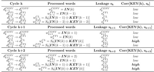
2.6 Power model at each clock cycle: the key dependence of the instan-taneous power consumption can be detected in the 2nd and the 3rd clock cycles. . . 76
3.1 Delta as a function of the input data in presence of different MF for a BUFF/INV gate. . . 110 3.2 Delta as a function of the input data in presence of different MF for
a AND/NAND gate. . . 110 3.3 Delta as a function of the input data in presence of different MF for
a OR/NOR gate. . . 110 3.4 Delta as a function of the input data in presence of different MF for
a XOR/NXOR gate. . . 110 3.5 Variation of the delay δ with the driving strength for different
mis-match factors. . . 111 3.6 Output delay in the AND/NAND gates (in ps). . . 113 3.7 Power balancing metrics for the registers under test. . . 127 3.8 Performances of the DPLs in terms of occupied area and average
energy under high output mismatch (MF = 3). . . 128 3.9 The DDPL065 cell library, designed using the CMOS065 technology. 139
4.1 Performances of the designed SABL and iDDPL circuits compared to CMOS. . . 162 4.2 Gate count for each core of the SERPAES chip after synthesis. . . . 190
5.1 Correlation between static power of the S-Box and the Hamming weight of the input/output words. . . 239 5.2 Leakage currents measured for the DPL crypto-cores as a function of
the input pattern. . . 242 5.3 Actual security metrics for the DPL crypto-cores (SNR = -20dB). . 246 5.4 Coefficient of variation (%) for the static currents distribution
mea-sured for the 100 crypto-core sample circuits designed with DPLs. . 251 5.5 Actual security metrics for the DPL crypto-cores successfully attacked
with a LPA procedure (SNR = -20dB). . . 252 5.6 Leakage currents measured for the iDDPL crypto-core as a function
of the output pattern. . . 256
6.1 Summary of the results of the experiments conducted on the AES cores implemented on the Cyclone FPGA in the workstation SCLab. 287
A.1 Boolean equations describing the 4x4 S-Box S0 of Serpent and the 4x4 S-Box of PRESENT. . . 295
List of Acronyms and
Abbreviations
ADLBL Asynchronous Directional Latch Based Logic
AES Advanced Encryption Standard
ALU Arithmetic Logic Unit
ASIC Application Specific Integrated Circuit
BCDL Balanced Cell-based Differential Logic
CAD Computer Aided Design
CCWSR Compile Characterize Write Script Recompile
CHES Cryptographic Hardware and Embedded Systems
CMOS Complementary Metal Oxide Semiconductor
CPA Correlation Power Analysis
CPLD Complex Programmable Logic Device
CPPR Clock Path Pessimism Removal
CQFP Ceramic Quad Flatpack
CRPR Clock Reconvergence Pessimism Removal
CTS Clock Tree Synthesis
CV Coefficient of Variation
DB Database
DC Design Compiler
DDPL Delay-based Dual-rail Precharge Logic
DES Data Encryption Standard
DLL Delay Locked Loop
DPA Differential Power Analysis
DRC Design Rule Check
DRSL Differential Random Switching Logic
DTS Dynamic Timing Simulation
DUA Device Under test
EDA Electronic Design Automation
EEPROM Electrically Erasable Programmable Read Only Memory
EMA Electromagnetic Analysis
FED Frequency Energy Deviation
FFT Fast Fourier Transform
FN Feistel Network
FPGA Field Programmable Gate Array
FUB Fondazione Ugo Bordoni
GE Gate Equivalents
GIDL Gate Induced Drain Leakage
HD Hamming Distance
HDL High Description Language
HVT High Voltage Threshold
HVTGP High Voltage Threshold General Purpose
HW Hamming Weight
iDDPL improved Delay-based Dual-rail Precharge Logic
IO Input Output
ISCOM Istituto Superiore delle Comunicazioni e dell’Informazione
LEF Library Exchange Format
LFSR Linear Feedback Shift Register
LIB Liberty
LPA Leakage Power Analysis
LUT Look Up Table
LVS Layout Versus Schematic
LVT Low Voltage Threshold
MDPL Masked Dual-rail Precharge Logic
MF Mismatch Factor
MIA Mutual Information Analysis
MTD Measurements To Disclose
NED Normalized Energy Deviation
NSD Normalized Standard Deviation
PAA Power Analysis Attack
PBC Point Biserial Correlation
PC Personal Computer
PD Pull Down
PDA Personal Digital Assistant
PLL Phase Locked Loop
PSD Power Spectrum Density
PSN Power Supply Network
PU Pull Up
RAM Random Access Memory
RFID Radio-Frequency Identificator
RNG Random Number Generator
ROM Read Only Memory
RTZ Return To Zero
SABL Sense Amplifier Based Logic
SAFF Sense Amplifier Flip Flop
SCA Side Channel Attack
SCLab Smart Card Laboratory
SDB Synopsys Database
SDC Synopsys Design Constraints
SDF Standard Delay Format
SIMD Single Instruction Multiple Data
SNR Signal to Noise Ratio
SoC System on Chip
SPA Simple Power Analysis
SPN Substitution Permutation Network
SR Single Rail or Set Reset or Success Rate
STA Static Timing Analysis
SVT Standard Voltage Threshold
TA Template Attack
TDPL Three-phases Dual-rail Precharge Logic
TEL Time Enclosed Logic
USB Universal Serial Bus
VHDL VHSIC Hardware Description Language
VHSIC Very High Speed Integrated Circuit
VLSI Very Large Scale Integration
Introduction
Scientific context
The main features of modern cryptography are entangled in these words [40]:
"A security system is as strong as its weakest part".
Every cryptographic design should be conceived with these words in mind. In general, a security system is composed of several parts, and the property of the weakest element fixes the constraints of the entire system. In order to guarantee a minimum level of security, identifying the weakest element(s) and improving its (their) strength are crucial issues.
By the end of 1970s when the Diffie-Hellman exchange protocol was proposed [80] and the public key cryptography was introduced, the main challenge of cryptog-raphers was to develop new algorithms to encrypt secret data in the most secure and effective way. In the same years, the Data Encryption Standard (DES ) was invented [35]. With the standardization of DES, symmetric key cryptography started to become established. DES was the standard for several years, until its mathematical strength was demonstrated to be low for modern computational machines. By the end of 1990s, a second generation of cryptography was developed: efficiency and speed were now considered as fundamental as security. The Advanced Encryption
Standard (AES ) is the supreme outcome of that period [2]. AES links together the
benefits of a secure encoding with high performances, without sacrificing elegance, therefore it is widely considered as the best block cipher ever invented. Even if AES represents an efficient solution still nowadays, in very last years with the technology progress cryptography has taken a new direction, leading to the beginning of a novel era: increasingly, everyday items are enhanced to pervasive devices by embedding computing power. Smart-cards, RFID tags, medical devices, transport and payment cards, car immobilizers, PDA’s are common examples. The interconnection of these pervasive devices leads to the famous vision of ubiquitous computing (ubicomp) introduced by Mark Weiser [128]. A widely shared view is that ubiquitous computing is the next paradigm in information technology, thus encapsulating information in ever more cheap, lightweight, and easy to carry out devices has become a trend. If early cryptographers thought that the strength and the effectiveness of a crypto-graphic application could be reached by designing a robust mathematical algorithm, in modern cryptography the perfection associated to the mathematics is leaving ever more space to the imperfect pragmatism of physical implementations.
element of the system is not anymore the cryptographic algorithm, but the imple-mentation which runs the algorithm itself. This had the effect of changing the vision of security, such that today the physical implementation is considered as the weakest element of the system: in other words, an ideally secure cryptographic algorithm can be insecure in practical applications because of the vulnerability of the host device. The latter is an electronic device which maps the message and an internally stored key into a ciphertext. During the encryption, data are physically manipulated within the device in form of electric signals, bringing part of information to leak out during the computation through additional unpredicted information channels which fluctuate in a hostile environment and can be captured by an adversary. These information channels are widely known as side channels. Noise, light, consumed power, electromagnetic emissions, and any other perturbation are examples of side channels [112]. The dangerousness of these unintentional physical emissions is in the fact that they can be exploited by the adversary to extract secret information from the device. An attempt to steal information by a cryptographic device is called in the context of cryptography as Side Channel Attack (SCA) [61].
In last years, limiting the amount of information leaked by side channels has become a preeminent issue in the design of cryptographic circuits. Very often, the presence of side channels is investigated and possibly prevented through critical and penetrating analysis. Several research groups have started to investigate algorith-mic and physical countermeasures to these threats, as well as new possible attack methodologies in order to demonstrate the effectiveness of an implementation or the vulnerability of another one. In this context, the technology progress plays a crucial role, given that several implementations, formerly defined secure, were proved to be highly unsafe, with a negative commercial and economical impact for the manufacturing companies. In some sense, it is just like an arms race between hackers and manufacturers, as well as researchers and researchers, in a sort of everyone against everyone. Clearly, research in this field is of primary interest for all the actors.
Objective and motivation to this work
In accordance to the above discussion, this thesis work has been conceived in the scenario of physical observable cryptography [82]. Physical observable cryptography is a relative recent discipline dealing with the problems of physical security, which were not considered by traditional cryptography [115]. It links together the issues related to the design of digital VLSI circuits with security aspects, under the perspective of providing a final product which exhibits a relatively low physical leakage. According to this definition, physical observable cryptography is intended with the purpose of building secure and efficient cryptographic devices, by integrating a specific crypto-graphic algorithm with a series of circuit improvements in order to ensure a sufficient level of security of commercial devices. Although no general theory has been still rigorously formulated, a lot of sub-fields have been developed, ranging from the design of digital cryptographic circuits, up to the definition of advanced statistical tools for the exploitation of the information leakage.
heterogeneous disciplines, and involves the collaboration of experts of different areas: on a side, digital designers have the role of investigating every possible origins of physical leakage in modern technologies; on the other side, security experts must be able to integrate statistical and mathematical metrics for the evaluation of the leakage already during the earlier steps of the design, in order to provide the digital experts with efficient tools to define the design constraints. The question arises when different technologies are used to implement a cryptographic primitive: in other words, the level of security of a specific implementation designed some years ago can be dramatically different from the level of security of the same implementa-tion designed today using a different technology. Furthermore, an implementaimplementa-tion evaluated and defined as secure some years ago, can be cracked today with more powerful and advanced attack instruments.
Actually, it is impossible to face all the issues related to physical observable cryptography. For this reason, in this thesis work we focus on a specific aspect: the analysis and the design of cryptographic integrated circuits for portable embedded devices (e.g. smart-cards), designed with modern electronic nanotechnologies, which are able to counteract SCAs through an improved hardware security. More specifi-cally we discuss and define novel methodologies and design-time metrics to build circuits able to thwart a specific subset of SCAs, Power Analysis Attacks (PAAs), which are a class of attacks targeting the power consumption of a device as side channel [62].
In this context, this work has been addressed towards the design of hardware countermeasures against PAAs, which have the purpose of improving the level of security of a circuit already at physical level. A key problem in the design of cryptographic circuits in modern technologies is linked to the unavoidable electrical mismatches arising in submicron region, which are the physical reasons that make the instantaneous power consumption of a CMOS circuit dependent on the internal processed data. The electrical mismatches are expected to increase with the tech-nology scaling, and require to re-define the level of security of previously proposed countermeasures as well as adequately address the strength of novel countermeasures. In this regard, capacitive and timing mismatches on the internal interconnect wires represent of course the most important leakage sources. In literature many efforts have been made towards the design of well-balanced interconnections in crypto-graphic circuits in order to mitigate these effects and equalize the power consumption. For this purpose several layout optimizations and assisted routing methods have been presented, but these techniques have the disadvantage of requiring a customized design flow; furthermore, they proved to be suboptimal, because process mismatches are very difficult to be controlled; moreover, the electrical mismatches are expected to increase with the technology scaling.
In addition to the problem of the electrical mismatches, recent research in the field of PAAs demonstrated that also the static power consumption, which was not considered in early works on PAAs, can be adopted as actual leakage source in submicron circuits. Leakage power in CMOS devices is expected to increase with the technology scaling, posing new requirements not only on the design of low-leakage electronic circuits, but also on the assessment of the level of security of nanoscaled crypto-devices.
Description of the adopted tools
The main part of the work presented in this thesis has been performed in simulation, using some of the most known CAD tools widely adopted for the design of electronic circuits. The simulation results and the discussion presented in this thesis prove the relevance of electronic simulations in the context of security design. The most important outcome of this work has been the design of a cryptographic ASIC in CMOS 65nm using a semi-custom design flow in simulation. The chip contains a number of cryptographic cores (e.g. AES and Serpent) implementing some countermeasures developed in our department in last years, which have been extensively evaluated in simulations.
Most of the simulations presented in this work have been executed in the Cadence
Virtuoso Analog Design Environment on Linux Fedora operating system. Layout,
physical verification, extraction and back-annotation of the critical parts have been executed with the Virtuoso Layout Editor Suite, using the integrated Calibre processor for parasitics extraction.
The digital design flow for the cryptographic ASIC has been executed using
Synopsys DC Compiler for Register Transfer Level (RTL) synthesis (front-end flow)
and Cadence SoC Encounter for the place and route (back-end flow). Furthermore, functional simulations in the early steps of the project have been performed using
Altera Quartus II, and repeated in post-layout using Cadence NCSim.
In addition, Matlab has been used for post-processing and calculation, and
Labview has been adopted to control the oscilloscopes in practical activities.
Description of the technology process node
The electrical scheme as well as the layout presented in this thesis work have been designed using the 65nm Bulk CMOS (CMOS065) Process provided by ST
Microelectronics. In this paragraph we provide some general information about the
technology and the transistor models used in this work [117].
The design kit provided by the semiconductor vendor allows to choose the stan-dard or the advanced process. We have used the stanstan-dard option, which is composed of two possible alternatives: the Low Power (CMOS065_LP) and the Low Power with access to General Purpose (CMOS065) transistors models. The CMOS065_LP process serves battery operated and wireless applications; it is characterized by a single IO oxide plus a single core oxide dual Vtprocess, and uses copper metallization
with 7 metal layers (5 thin plus 2 thick) and low-k dielectrics. The CMOS065_LPGP is a single IO oxide plus dual core oxide dual Vt process, and uses copper metalliza-tion with 7 metal layers (5 thin plus 2 thick) and low-k dielectrics.
Both the above described processes give access to the following add-on options: the Low Vt (LVT), the Standard Vt (SVT), and the High Vt (HVT) transistors. They differ from the value of the threshold voltage. The LVT devices switch faster, but have the penalty of exhibiting higher static leakage power. On the contrary, the HVT devices switch slower, but have the advantage of reducing the static leakage power. The SVT devices represent an efficient compromise for general applications. The power supply of the transistors differ according to the processes: the
CMOS065_LP process has a 1.8nm thin oxide, is designed for 1.2V (±10%) applica-tions (max 1.32V) with 1.8V or 2.5V capable IO pads; the CMOS065_LPGP process has a 1.3nm thin oxide, is designed for 1.2V (±10%) applications (max 1.32V) with GP devices limited to 1.0V (±10%) (max 1.1V) and with 1.8V (±10%) or 2.5V (±10%) capable IO pads. The 1.8V IO pads have a 2.8nm thick oxide, and are targeted for a maximum voltage of 1.98, whereas the 2.5V IO pads have a 5.0nm thick oxide, support an overdrive supply voltage of 3.3V, and are target for a maximum voltage of 3.63V.
The natural drift devices are targeted for nominal power supply voltage of 8V on the drain (|Vds| ≤ 8V ), and, accounting for a tolerance of (±10%), they are qualified for a maximum voltage of 8.8V on the drain.
Outline of the thesis
This thesis is divided in 7 chapters, which deal with electronics and cryptography issues and are strongly related.
In Chapter 1, an in-depth discussion about the topic of hardware security is provided. More specifically, we introduce the reader to the concept of physical security in nanoscaled cryptographic circuits. For this purpose, after discussing some basic foundations related to the design of integrated circuits for specific applications (ASICs) in deep-submicron technologies, the theory on SCAs is recalled, with a par-ticular emphasis on PAAs. The analysis of PAAs and the design of countermeasures against PAAs is the guideline of this work. In this chapter we discuss also a basic standard procedure to design secure cryptographic circuits for hardware-oriented cryptographic primitives.
In Chapter 2 we present the Time Enclosed Logic (TEL) circuits as a hardware-level countermeasure to counteract PAAs in submicron circuits. This countermeasure is based on a novel digital data encoding and a specific design methodology, which can be integrated using common CAD tools for SPICE-level simulations and layout. Furthermore, we present a new design-time metric to assess the intensity of the leakage emission of cryptographic circuits. A case study cryptographic circuit, named in this thesis SERPENT-block, has been implemented using this countermeasure, and the PAAs resistance of such an implementation has been validated through extensive SPICE simulations.
In Chapter 3 we describe a full custom implementation of the TEL concept: the improved Delay-based Dual-rail Precharge Logic (iDDPL) style. A prototype standard-cell library of iDDPL gates has been used to design the SERPENT-block. More specifically, the logic gates composing the library are based on a specific circuit template and have been optimized down to the layout level by overcoming the electrical mismatches arising in submicron devices, which are well known to reduce the level of security of cryptographic circuits. In this chapter a discussion about the adoption of this prototype digital library in a standard semi-custom design flow is also provided.
In Chapter 4 we present the design of a prototype cryptographic ASIC, the
SERPAES chip. This chapter is more digital design oriented, and provides an
CAD tools. Different independent cryptographic cores developed in our department and previously evaluated with respect to PAAs resistance are implemented on the chip. Among them, the SERPENT-block evaluated in Chapter 2 and implemented with the standard-cell library presented in Chapter 3 is described in minute detail. All the design steps as well as the design choices are discussed and described in order to understand the main issues of the project.
In Chapter 5 we recall the topic of Leakage Power Analysis (LPA) attacks. LPA attacks exploit the leakage arising from the static power consumption of deep-submicron circuits, which is correlated to the processed data and is expected to further increase with the technology scaling. We demonstrate on some specific case studies the feasibility of this new class of attacks and their dangerousness for embedded devices. As additional contribution, we investigate the LPA resistance of the countermeasure presented in previous chapters, and we demonstrate that it represents a promising solution also to prevent LPA attacks.
Chapter 6 is dedicated to the description of some experimental activities exe-cuted as an integration of this research. We have implemented two measurement workstations for implementing PAAs. The first setup has been mounted in order to evaluate the security of the SERPAES chip designed during the research activity. The measurement workstation is located in the laboratory of our department, where the SERPAES board on which the chip is hosted has been connected. At the moment of writing this work, the SERPAES chip has been proved to be fully functional, whereas the PAAs experiments are going to be performed. The second setup has been designed in the laboratories of the Ministry of Economic Development, where other countermeasures designed in our department have been evaluated on a FPGA. In Chapter 7 we draw the conclusions to this work and discuss some possible developments as future improvement to these activities.
Contents
Introduction xvii
1 Physical security in submicron technologies 1
1.1 Introduction . . . 1 1.2 Foundations on ASIC design . . . 2 1.2.1 Digital design flow strategies for VLSI circuits . . . 2 1.2.2 ASIC vs FPGA . . . 3 1.2.3 Description of the semi-custom design flow for ASIC . . . 4 1.2.4 Main issues in the design of submicron integrated circuits . . 5 1.3 Physical security of cryptographic circuits: a review of Side-Channel
Attacks (SCAs) . . . 8 1.4 Origin of leakage in submicron technologies . . . 10 1.4.1 Power consumption of CMOS circuits . . . 10 1.4.2 Electromagnetic field irradiated by CMOS circuits . . . 15 1.5 Power Analysis Attacks (PAAs) . . . 17 1.5.1 Standard methodology to implement PAAs . . . 17 1.5.2 Differential Power Analysis (DPA) . . . 21 1.5.3 Correlation Power Analysis (CPA) . . . 21 1.5.4 Template Attacks (TA) . . . 22 1.6 Symmetric cryptography for SCAs evaluation . . . 23 1.6.1 Block ciphers as cryptographic case study . . . 23 1.6.2 Review of two basic block ciphers: Rijndael and Serpent . . . 24 1.6.3 Lightweight cryptography: the PRESENT block cipher . . . 29 1.7 Design strategies for secure block ciphers . . . 31 1.7.1 Hardware properties of cryptographic primitives . . . 31 1.7.2 Building blocks of cryptographic circuits . . . 32 1.7.3 Hardware countermeasures against PAAs: a survey . . . 33 1.7.4 Metrics to compare the efficiency of hardware implementations 35 1.8 Overview of Dual-Rail Precharge Logic (DPL) styles to counteract
PAAs . . . 36 1.8.1 General description of DPLs . . . 36 1.8.2 Limitations of DPL styles in submicron technologies . . . 37 1.8.3 A comparison among some popular DPLs . . . 40 1.8.4 The secure digital design flow for cryptographic ASIC based
on DPLs . . . 40 1.9 Conclusion . . . 42
2 Time Enclosed Logic: a hardware countermeasure to overcome
PAAs 45
2.1 Introduction . . . 45 2.2 Security assessment of hardware countermeasures . . . 46
2.2.1 Assumptions on the adversary model adopted for the PAAs procedure . . . 46 2.2.2 Metrics for the evaluation of the physical leakage . . . 47 2.3 A novel data encoding for differential dynamic cryptographic circuits 50 2.3.1 Brief review of Return To Zero (RTZ) logics . . . 50 2.3.2 Basic principle of Time Enclosed Logic (TEL) circuits . . . . 51 2.4 Description of TEL circuits . . . 53 2.4.1 Cell templates for TEL circuit implementations . . . 53 2.4.2 A first-order model of the dynamic power consumption . . . . 55 2.4.3 Timing constraints of a TEL circuit . . . 58 2.4.4 The fluctuation effect of the delay δ . . . 60 2.4.5 Second order effects: transient leakage . . . 61 2.4.6 Energy balancing and timing enclosing properties . . . 64 2.5 A balancing act: frequency analysis of the current traces . . . 65 2.5.1 Insertion of an on chip filter in a TEL circuit . . . 65 2.5.2 A new frequency-based metric . . . 66 2.5.3 Relation between δ and f0 in a TEL gate . . . 69 2.6 A cryptographic case study . . . 70 2.6.1 The SERPENT-block . . . 70 2.6.2 Description of the architecture of the circuit . . . 72 2.6.3 Direct analysis of the power model of the pipeline . . . 73 2.6.4 Estimation of the cutoff frequency f0 of the circuit . . . 76 2.7 Security evaluation of the TEL circuit . . . 77 2.7.1 Design of the on-chip filter considering chip peripherals . . . 78 2.7.2 Area estimation of the countermeasure . . . 79 2.7.3 Evaluation of the leakage of the noise-free current traces . . . 79 2.7.4 Correlation Power Analysis attacks with Gaussian noise . . . 81 2.8 Conclusions . . . 85
3 An ASIC-oriented implementation of TEL circuits 89
3.1 Introduction . . . 89 3.2 The Improved Delay-based Dual-rail Precharge Logic family . . . 90 3.2.1 A full custom circuit implementation of TEL . . . 90 3.2.2 Limitations of the Delay-based Dual-rail Precharge Logic
(DDPL) style . . . 91 3.2.3 Cell template of an iDDPL gate . . . 91 3.2.4 Conversion of the signal from the CMOS domain . . . 94 3.2.5 Design-time metrics and simulation parameters . . . 97 3.3 Design and characterization of iDDPL combinational gates . . . 99 3.3.1 Fluctuation effect in iDDPL gates . . . 99 3.3.2 Analysis of the early evaluation effect . . . 100 3.3.3 Combinational gates with capacitive load imbalance . . . 108 3.3.4 Presence of mismatch variations . . . 111
3.3.5 Validation of the model in some case study combinational gates112 3.4 Design and characterization of an iDDPL sequential element . . . 116 3.4.1 Main issues in the design of DPL sequential elements . . . 116 3.4.2 A master slave flip-flop for the iDDPL style . . . 118 3.4.3 Simulation and comparison of some DPL 4-bit registers . . . 122 3.5 The prototype iDDPL library . . . 128 3.5.1 Architecture of a micropipelined iDDPL circuit . . . 128 3.5.2 Analysis of the timing constraints . . . 129 3.5.3 Layout of the iDDPL cells . . . 134 3.5.4 Consideration on the layout of the flip-flop . . . 135 3.5.5 The DDPL065 cell library . . . 138 3.6 Conclusions . . . 139
4 Design of the SERPAES prototype chip 141
4.1 Introduction . . . 141 4.2 Design of the SERPENT-block . . . 142 4.2.1 Full custom design methodology . . . 142 4.2.2 Data-path of the circuit . . . 143 4.2.3 Design of the iDDPL sub-block . . . 144 4.2.4 Design of the SABL sub-block . . . 159 4.2.5 Design of the complete SERPENT-block . . . 162 4.3 Description of the AES-block . . . 164 4.3.1 From FPGA to ASIC . . . 164 4.3.2 Architecture of the AES-block . . . 166 4.3.3 The basic AES encryption unit (AES-0) . . . 167 4.3.4 The random precharged interleaved pipeline countermeasure
(AES-1) . . . 168 4.3.5 The random interleaved pipeline countermeasure (AES-2) . . 169 4.3.6 The XOR-series countermeasure (AES-3) . . . 169 4.3.7 The XOR-parallel countermeasure (AES-4) . . . 170 4.4 Logic synthesis of SERPAES . . . 170 4.4.1 General information on the synthesis methods in DC . . . 171 4.4.2 Synthesis design flow for SERPAES . . . 173 4.4.3 Preliminary steps before the synthesis . . . 174 4.4.4 Logic synthesis of the AES-block . . . 178 4.4.5 Logic synthesis of the SERPAES chip . . . 182 4.5 Place and route of SERPAES . . . 192 4.5.1 Standard-cell layout . . . 192 4.5.2 Digital back-end flow . . . 192 4.5.3 General settings . . . 194 4.5.4 Floorplan . . . 195 4.5.5 Static Timing Analysis . . . 200 4.5.6 Placement . . . 204 4.5.7 Post-placement optimization . . . 206 4.5.8 Clock Tree Synthesis (CTS) . . . 207 4.5.9 Post-CTS optimization . . . 209 4.5.10 Routing . . . 210
4.5.11 Post-route optimization . . . 211 4.5.12 Signoff and final verification . . . 213 4.6 Testing the functionality of SERPAES . . . 215 4.6.1 Design of the SERPAES board . . . 215 4.6.2 First measurements on the chip . . . 215 4.7 Conclusions . . . 218
5 Leakage Power Analysis attacks against nanoscaled DPL circuits 221
5.1 Introduction . . . 221 5.2 Review of Leakage Power Analysis attacks . . . 223 5.2.1 Context of LPA attacks . . . 223 5.2.2 Leakage model for bit-slice structures . . . 225 5.2.3 Standard procedure for LPA attacks on bit-slice circuits . . . 225 5.2.4 Some considerations about noise in practical LPA attacks . . 226 5.2.5 Security metrics to assess the vulnerability on the static power 227 5.3 Leakage current in combinational gates in CMOS 65nm . . . 229 5.3.1 Evaluation of the variability of the leakage of single logic gates 229 5.3.2 Standard CMOS logic . . . 229 5.3.3 Dual-rail Precharge Logic styles . . . 230 5.4 Leakage Power Analysis attacks and lightweight cryptography . . . . 233 5.4.1 Leakage model for a generic non-bit-slice structure . . . 233 5.4.2 Static power analysis methodology for a lightweight
crypto-graphic implementation . . . 235 5.4.3 Analysis of the static power of the combinational S-Box S0 . 237 5.4.4 Analysis of the static power of the SERPENT-block . . . 241 5.4.5 LPA attacks against the crypto-processor considering noise . 242 5.5 Evaluation of the LPA effectiveness with power variability issues . . 248
5.5.1 Impact of intra-die and inter-die process variations on the actual security metrics adopted in LPA . . . 248 5.5.2 Impact of intra-die variation on the leakage model . . . 249 5.6 Investigation on the static power variability in TEL circuits . . . 251 5.6.1 Practical considerations on LPA attacks against TELs . . . . 251 5.6.2 Leakage distribution on single iDDPL gates . . . 254 5.6.3 Leakage model of an iDDPL circuit . . . 254 5.6.4 LPA attacks . . . 257 5.7 Conclusion . . . 258
6 Practical evaluation of PAAs against cryptographic circuits 261
6.1 Introduction . . . 261 6.2 SESAMO project: evaluation of the hardware security of
crypto-graphic devices . . . 261 6.2.1 Objective of this activity . . . 261 6.2.2 Description of the measurement setup SCLab . . . 262 6.2.3 Description of the cryptographic cores used in the experiments 271 6.2.4 Description of the experiments . . . 274 6.3 Conclusions . . . 287
7 Conclusions and final remarks 289
7.1 Relevance of full-chip simulations and design-time evaluation in chip-card manufacturing . . . 289 7.2 Summary of the research contribution . . . 290 7.3 Future directions and improvements . . . 292
A Implementation of 4x4 S-Boxes 295
Chapter 1
Physical security in submicron
technologies
1.1
Introduction
Following the considerations done in the introduction to this thesis, the most important question in physical observable cryptography is how the security level of a cryptographic device re-maps in modern technologies. The trend of reducing dimension and power consumption of a circuit leads to the need of re-evaluate and possibly update the level of security of the entire system. Indeed, physical leakage of a certain implementation designed some years ago can be dramatically different from the leakage of the same implementation designed with a more modern technology. The reason is that the devices are optimized under the perspective of improving the performances in terms of area and power, but these improvements do not take security into account.
In this chapter we recall some introductory concepts about digital design flow and cryptography, with the purpose of highlighting the main issues of hardware security for practical applications. Under this perspective, we first provide a brief introduction to the digital VLSI design; more specifically, we will focus on the ASIC design, which is probably the most useful design methodology to describe, in order to better understand and address the most relevant issues about hardware security. After describing the standard design flow for digital circuits, we introduce the topic of physical attacks against cryptographic circuits, with a particular emphasis on Side
Channel Attacks (SCAs) [61]. Among SCAs, we focus on Power Analysis Attacks
(PAAs) [62], which are the most common and popular examples of SCAs and have been chosen as guide line theme of this thesis work. Then, we will recall some well-known symmetric key encryption schemes as case studies, and the hardware design strategies to build secure digital implementations. Under this perspective, we will provide a brief discussion on the most common countermeasures against PAAs, with a particular focus on circuit level countermeasures, which are based on the adoption of a specific circuit architecture at cell level. For this purpose, we will show that in order to obtain a secure cryptographic circuit, the standard digital design flow needs to be rearranged by introducing some additional steps, which allow to enhance the level of hardware security of the chip, conducting to the so called secure
digital design flow.
1.2
Foundations on ASIC design
1.2.1 Digital design flow strategies for VLSI circuits
The exponential growth of the scale of integration, exemplified by the Moore’s law [84] (i.e. the increase in the number of transistors per unit area, or, more generally, the performance of the devices, doubling every 18 months), led to a radical innovation in the design flow of digital systems. If in the early 70’s the project was being carried by hand drawing the layout on large sheets of paper in accordance to the geometrical representation of the circuit on silicon, today this is no longer feasible due to the huge amount of active devices in the integrated circuits [101], which is represented by the acronym VLSI, Very Large Scale Integration.
The VLSI design represents the combination of two types of skills, architectural and circuital:
1. The architecture design skills correspond to the design of block diagrams modeled at various abstraction levels; they can comprise parts of software that must be performed by dedicated microprocessors or described in a hardware description languages (HDL). In this case, only the logical functionality is considered.
2. The circuit design skill consists in the connection of many transistors or logic cells, which are implemented at layout level through CAD tools. In this case, the electrical operation is taken into account.
In general, there are two typical approaches for the realization of digital circuits: full-custom and semi-custom.
In the full-custom (or, simply, custom) design the chip is implemented from
scratch, so that the individual blocks composing the system are designed up to the
transistor level. More specifically, in this design strategy no third parts modules are used, and all the entities are modeled and designed for that application. There are specific software tools which guide the designer along the custom project, allowing to semi-automate the layout of the chip and reduce the design time. Custom design has the advantage of optimizing the design in terms of power and performance, at the expenses of time and money. For this reason this approach is adopted mostly for the design of few functional blocks (e.g. floating point units and memory cells) or in general for a large number production.
The semi-custom design instead makes use of logic circuits that have already been implemented, usually by third parts. They can be divided into two categories:
cell-based or pre-fabricated units and array-based or pre-designed elements. FPGA,
Sea of Gate, PLD, CPLD are all examples of array-based elements. Among the cell-based units, three different design strategies can be categorized: standard-cells based, macro-cells based and compiled-cells based.
In the standard-cells based design, each cell corresponds to an elementary com-ponent, such as a logic gate or a flip-flop, or slightly more complex blocks such as multiplexers or other arithmetic circuits (i.e. full-adder). For every technological
Figure 1.1. A schematic representation of the different possible methodologies to design
digital VLSI circuits.
process there is a cell library composed of a number of logic gates characterized up to the layout level. In macro-cell based design, each macro-cell corresponds to a complex block such as an Arithmetic Logic Unit (ALU) or a register-file, but also small CPUs or memory banks. Finally, the compiled-cell based design is charac-terized by the usage of a particular class of standard-cells and macro-cells, which are automatically generated by means of suitable design tools in accordance to the technological process that the designer wants to use, but not described at layout level. The above discussed design strategies are represented in the diagram of Fig. 1.1.
1.2.2 ASIC vs FPGA
Cryptographic primitives as any other digital circuit can be implemented in both software and hardware, according to the target applications. In this paragraph an overview on the possible cryptographic implementations is briefly discussed [63].
Software implementations are designed and coded in programming languages, such as C, C++, Java, and assembly language, to be executed, among others, on general purpose microprocessors, digital signal processors, and smart-cards. Implementing a cryptographic algorithm in software was typical in the first era of cryptographic smart-cards, given that the flexibility of microcontrollers is suitable for portable applications.
The technology scaling as well as new issues in the field of hardware security facilitated a new hardware-oriented approach, with the development of new optimized algorithms for ultra-constrained devices (e.g. RFID tags). Hardware implementations are in general designed and coded in hardware description languages, such as VHDL and Verilog HDL, and are intended to be realized using ASIC or FPGA.
ASICs are designed all the way from the behavioral description down to the physical layout and then sent for a fabrication in a semiconductor foundry. FPGAs can be bought off the shelf and reconfigured by designers themselves. With each reconfiguration, which takes only a fraction of a second, an integrated circuit can perform a completely different function. FPGA consists of thousands of universal reconfigurable logic blocks, connected using reconfigurable interconnects and switches. Additionally, modern FPGAs contain embedded higher-level components, such as memory blocks, multipliers, multipliers–accumulators, and even microprocessor cores. Reconfigurable input/output blocks provide a flexible interface with the
outside world. Reconfiguration, which typically lasts only a fraction of a second, can change a function of each building block and interconnects among them, leading to a functionally new digital circuit.
As anticipated in the introduction, in this thesis work we focus on the design of cryptographic ASICs. Basically there are two strategies to design an ASIC: using a full custom design flow or a semi custom design flow. According to the discussion in previous paragraph, in the first case the circuit is implemented by designing each single functional units down to the transistor level, whereas in the second case the standard-cells available in a specific technology library are used.
In the following section we are going to describe more in detail the design of an ASIC following a semi-custom design approach.
1.2.3 Description of the semi-custom design flow for ASIC
An ASIC corresponds to a digital system conceived to perform a specific task. In general, it differs from SoC (System on Chip) by the fact that, while in an ASIC the designer tends to design "from scratch" the large part of the system, in the SoC he/she tries to reuse macro-blocks that are available from foundry handbooks. Furthermore a SoC can be used to carry out multiple functions, whereas an ASIC is used to execute a single activity (such as numerical signal processing, fingerprints detection, etc). Today, thanks to the technological improvements, the boundaries between these two device typologies have largely vanished, so many modern SoCs integrate some functional blocks conceived for specific task execution. At the same time, most ASICs contain CPUs and other general-purpose parts, so a modern ASIC is also a SoC and viceversa.
The design flow of a digital ASIC consists of the following key points [101]:
1. Architectural and electrical specifications: represented by an algorithm de-scribing what the system must do. At this level (“system level”), this attempts to identify what are the functional blocks which will make up the device, what they must to do, but there is no information on how they will do it. At this level also information relating to delays, power consumption, cost and clock frequency are known.
2. RTL coding in HDL: the RTL (Register Transfer Level) also called the archi-tecture level, lies a step below the system layer. After defining the system architecture, the designer will see in more detail how each module must carry out its own operations. The RTL specific returns, for each block, the processing performed on data and data transfers between the memory elements with the accuracy of the clock cycle. Today the specifications at RTL level are written using an Hardware Description Language (HDL).
3. Architecture Dynamic Simulation: it allows to evaluate the functionality of the specifications described in HDL. In particular, through the use of an appropriately designed testbench it will provide stimuli to the block to be simulated, and it will show if the data obtained are congruent to those expected. Dynamic simulation is performed with specific software, NCSim or ModelSim.
4. Design constraints and synthesis with standard cell: the design constraints such as frequency, maximum fan-out of the gates, delays, maximum area, etc. are defined. Then, each sub-block composing the system is synthesized using a specific software such as Design Compiler. The constraints are used to guide this tool in the synthesis.
5. Static Timing Analysis (STA) on each block: corresponds to the heart of the design of digital integrated circuits. The timing analysis allows to identify critical paths and improve them, estimate the maximum clock frequency achievable by the chip, thus identifying the "bottlenecks" of the architecture in order to eliminate them. Also for this step, there are specific programs.
6. Pre-layout static timing analysis: the timing analysis is performed on the whole project.
7. Initial floor-plan through cells guided placement: by means of STA a report file is generated with all constraints necessary to meet the specifications; this file allows to help the layout tool to place and route the cells.
8. Insertion of the clock tree.
9. Extraction of delays from the layout after the global routing, and consequent STA.
10. Detailed routing of the cells.
11. Extracting the actual delays by specific software, such as NCSim and Prime-Time.
12. Post-layout STA.
All these steps must be performed iteratively, so, for example, if the architectural simulation (step 3) is not satisfactory, the designer must return to the RTL coding (step 2) and reiterate the flow. So, in general, chip design is an iterative process, and it may happen that a single step must repeated several times, until all constraints are satisfied and everything is working properly. The block diagram of the digital flow is shown in Fig. 1.2.
1.2.4 Main issues in the design of submicron integrated circuits
The use nanometer CMOS technology encountered several problems when the active devices have been used to create complex digital systems such as ASIC and SoC using processes below 90nm. While I am writing this thesis, for the most advanced devices the scaling of transistors has arrived beyond the threshold of 20nm. The reduction of the size of active devices, combined with the increase in the number of levels of metal to be used for the interconnections, led to a higher density in the active area of integrated circuits and to a decrease of the switching delays of the logic elements. For this reason, now it is possible to integrate multiple functions in the same chip and achieve higher frequencies.
![Figure 2.22. Equivalent circuit model for the testbench in Cadence simulations [59]](https://thumb-eu.123doks.com/thumbv2/123dokorg/2892602.11343/106.892.210.725.182.368/figure-equivalent-circuit-model-testbench-cadence-simulations.webp)