Randomized Network of Single Walled Carbon
Nanotubes Thin Film Transistor: Fabrication,
Simulation and Application as Biosensor
BySayed Alireza Mousavi
A Thesis submitted in partial fulfillmentof the requirements for the degree of
Doctor of Philosophy in Physics
Approved Thesis Committee Approved Thesis Committee University of Salerno Jacobs University Bremen Prof. Vincenzo Tucci Prof. Veit Wagner Prof. Veit Wagner Prof. Vincenzo Tucci Prof. Giuseppe Milano Prof. Jürgen Fritz Prof. Danilo Roccatano Prof. Patrizia Lamberti Date of Defense:
28/10/2013
I
Contents
Abstract...2
Motivation and Objective...3
Chapter 1 Carbon nanotubes: Properties and Structure ... 6
1.1 Carbon Nanotube ... 6
1.1.1 Overview ... 6
1.1.2 Carbon nanotube structure: SWCNT & MWCNT ... 7
1.2 Electronic Properties of Carbon Nanotubes ... 10
1.2.1 Band Structure of Graphene ... 10
1.2.2 Metallic and Semiconducting SWCNTs... 12
1.3 Fabrication and Modelling Device based on Carbon Nanotube .. 15
1.3.1 Carbon Nanotube Electronics Device ... 15
1.3.2 Carbon Nanotube Bio/chemical sensing ... 20
1.3.3 Modelling of Carbon Nanotube Device ... 21
2 Chapter 2 State-of-the-art ... 23
2.1 Synthesis of Single Walled Carbon Nanotubes by Chemical Vapor Deposition ... 23
2.2 Single Walled Carbon Nanotubes Solution and Preparation ... 24
2.3 Deposition Methods for SWCNTs Solution ... 27
2.3.1 Spray Coating... 28
2.3.2 Dip Coating ... 28
2.3.3 Spin Coating ... 29
2.3.4 Dielectrophoresis Deposition ... 30
2.3.5 Electrophoretic Deposition ... 31
3 Chapter 3 Experimental Process for Fabrication of SWCNTs-TFT ... 33
3.1 Dispersion Process of Semiconducting SWCNTs on Aqueous Solution ... 34
II
3.1.1 Experimental Process for Fabrication Drain-Source Electrode
in the form of Interdigitated Electrode ... 37
3.1.2 Silanization of Substrate ... 38
3.1.3 Vacuum Filtration Deposition ... 39
3.1.4 Electrical Characterization of 90% Semiconducting SWCNTs-TFT 40 3.2 Experimental process for fabrication Thin Film Transistors by 99% Semiconducting Singe Walled Carbon Nanotube ... 45
3.2.1 Deposition Process and surface characterization ... 45
3.2.2 Electrical characterization of 99% semiconducting SWCNTs-TFTs by vacuum filtration deposition ... 46
3.2.3 Effect of Channel Length of 99% semiconducting SWCNTs-TFTs 50 4 Chapter 4 Numerical modelling of SWCNTs-TFTs ... 54
4.1 3-D Modelling of SWCNTs-TFTs ... 54
4.1.1 Representation of the SWCNTs aggregation ... 56
4.1.2 Electrical resistance of the thin-film by means of an equivalent electrical network ... 57
4.1.3 Simulation result of electrical properties of SWCNTs-TFTs .. 59
5 Chapter 5 Fabrication label-free biosensor based SWCNTs-TFT ... 63
5.1 Interaction between biotin-streptavidin ... 65
5.2 Immobilization procedure for deposition biomolecule on SWCNTS-TFT ... 66
5.3 Experimental result for biosensor ... 67
6 Chapter 6 Conclusion and future work ... 72
6.1 Conclusion ... 72
6.2 Future work ... 73
III
8 List of Publications ... 78 9 References ... 80
1
Abstract
Nanoelectronic devices based on nanomaterials, such as carbon nanotubes (CNTs) have attracted remarkable attention as a promising building block for future nanoelectronic circuits due to their exceptional electrical, mechanical and chemical characteristics. The electrical characteristics of CNTs, such as high mobility, quasi-ballistic conductance and resistance against electromigration, allow to surpass the properties of current Si based complementary metal oxide semiconductor (CMOS) devices. In particular, the large surface area and nanoscale structure makes SWCNTs promising candidates for chemical and biological sensing applications as well. Current research covers broad scientific fields, such as study of materials properties at nanoscale, development, fabrication and simulation of nanoscale structures, for electronics and biomedical applications. However, there is ample space for advancements in both theoretical studies and practical applications for CNT-based systems.
This thesis addresses the design and manufacture of thin film transistor (TFT) based on randomized network of single walled carbon nanotubes (SWCNTs) that exploit the unique properties of such materials to create a label-free biosensor for detection of variety biomolecules, particularly proteins. In addition, in order to analyze the electric transport of SWCNTs network in the TFT channel a numerical 3-dimensional (3D) model for the thin film layer is developed.
The SWCNTs-TFTs are fabricated by using microfabrication to obtain a micro-interdigitated electrode (μ-IDE) as drain-source electrode. The sizes vary between 2 to 50 µm. Thin-film transistors (TFTs) are fabricated by using SWCNTs thin film as the semiconducting layer and SiO2 thin film as the dielectric layer. The
high purity semiconducting network of SWCNTs layer is deposited with an effective technique that combines the silanization of the substrate with vacuum filtration process from dispersed SWCNTs in surfactant solution. . The adopted technique provides a low-cost, fast, simple, and versatile approach to fabricate high-performance SWCNTs-TFTs at room temperature. The morphological arrangement of SWCNTs forming the active layer in the channel of the transistor is checked with scanning electron microscopic (SEM). The TFTs obtained exhibit p-type transistor characteristics and operate in
2
accumulation mode. The results are interpreted by considering the percolation theory. The exponent α of the power law describing the conductivity can be linked to the structural complexity of the SWCNT network. In particular an exponent = 1.7 was found experimentally, showing that the obtained thin film is relatively dense and near percolation. In addition, the experimental data have been compared with the results of the 3D model simulating the charge transport in the SWCNT structures formed in the TFT channel. The simulation results lead to an exponent = 1.8 that is in good agreement with the experimental data. The proposed model seems to be able to reliably reproduce the transport characteristics of the fabricated devices and could be an effective tool to improve the SWCNTs-TFTs structure. Moreover, the fabricated SWCNTs-TFT devices provide a suitable platform for high-performance biosensors in label-free protein detection. The sensing mechanism is demonstrated on a proof of principle level for the interaction of biotin and streptavidin on the SWCNTs surface. It is used as a research model for biosensor application. The SWCNTs thin-film biosensor has high sensitivity and it is capable of detecting streptavidin at concentration of 100 pM.
3
Motivation and Objective
Recently, low-dimensional materials have attracted great attention in the field of nanoelectronics for various applications e.g. integrated circuits (ICs) and sensing systems. Particularly, single walled carbon nanotubes (SWCNTs), due to exceptional electrical properties such as high mobility at room temperature are used for building nanoelectronic devices. Moreover, the large surface area and nano scale structure of SWCNTs makes them one of the most interesting materials for chemical and biological application.
Although a single carbon nanotube exhibits very high mobility, the fabrication of electronic devices such as field effect transistor (FET) based on carbon nanotubes is highly challenging and not technologically established for large area applications and scalable manufacturing devices. In addition, carbon nanotubes show heterogeneous electrical features such as mixture of metallic and semiconducting species. Moreover, they show different diameters and lengths. Furthermore, the synthesis carbon nanotubes require a high temperature environment which is not compatible with arbitrary substrate materials. To overcome these problems and meanwhile take advantage of such an exceptional nano-material, this work investigates the fabrication and electrical properties of thin film transistors (TFTs) based on randomized network of single-walled carbon nanotubes at room temperature. The devices are manufactured using a post-growth deposition technique. The fabricated SWCNTs thin film transistor is used as a transducer for bio-molecules detection, particularly as a label-free bio-sensor. The advantage of label-free bio-sensing compared to the labelled one is the fact that additional processes that can degrade sensitivity and alter the system response are avoided. Moreover, in order to investigate the electrical transport of SWCNTs network inside the channel of TFTs a 3D-numerical modelling is performed.
Bottom-gate TFTs were fabricated on a highly p-doped Si substrate with a thermally grown SiO2 layer (100 nm) as a gate dielectric. The
bottom source/drain electrodes in the form of interdigitated electrodes (IDEs) were fabricated by standard photolithography and lift-off processes. The feature sizes of the microstructures are varying between 2 to 50 µm. Subsequently, the thin film of SWCNTs is deposited with an effective technique that combines the silanization of
4
substrate with vacuum filtration process. High purity semiconducting SWCNTs are dispersed in surfactant solution and are deposited on the substrate with patterned electrodes. This technique provides a fast, simple, and versatile approach for fabrication of high-performance SWCNTs-TFTs at room temperature. The spatial arrangement in SWCNTs network was investigated by using a scanning electron microscope (SEM). The SWCNTs-TFTs exhibits p-type transistor characteristics. High purity semiconducting SWCNTs are used as an active layer in the channel of TFTs. They provide suitable platforms for high-performance biosensors. Particularly, functionalized SWCNTs surface with biotin is used to detect the protein, streptavidin (SA). The high purity semiconducting SWCNTs network has high sensitivity and it is capable of detecting SA at an ultra-low concentration of 100 pM.
In order to understand the transport properties of SWCNTs network, a numerical simulation has been developed using a 3D model. The channel of TFT structure is modelled as a random mixture of conducting cylinders. . The variation of electrical conductivity of the structure can be computed by implementing a 3D resistor network which includes resistors associated to the intrinsic resistance of SWCNTs and tunnelling effect between conducting clusters. By using a Monte Carlo analysis the behaviour of the electrical conductivity and the dependence of the percolation thresholds as a function of geometrical and physical influencing parameters can be analyzed. The results of numerical simulations are in good agreement with those obtained from the experimental characterization.
The research project carried out during the PhD program has been focused on three main aspects:
• Fabrication and electrical characterization of SWCNTs-TFTs.
• Development of an accurate numerical model which can be used to obtain information on the transport properties of randomized network of SWCNTs in the channel of TFT structure based on geometrical and physical properties of SWCNTs.
• Application of the SWCNTs-TFT as a transducer for a label-free biosensor for detection of a specific protein.
5 This thesis is organized as follows.
• In the first chapter a general overview on carbon nanotubes, properties, and the most promising applications of CNT is given.
• In the second chapter state of the art related to mechanisms of growing carbon nanotubes, experimental procedures to separate the semiconducting from metallic SWCNTs and various deposition technique are described.
• In the third chapter the fabrication procedure for making thin film transistor using a wet chemical of SWCNTs solution, the results concerning the electrical characterization on SWCNTs-TFTs containing different concentrations of semiconducting SWCNTs are described in detail. In addition, the morphological arrangement of SWCNTs network is investigated.
• Chapter 4 provides an overview on the models available in the literature and then presents the numerical model that has been implemented. A detailed description of the modelling of SWCNTs-TFT based on a 3-dimensional (3D) model, both in terms of geometric approach and the optimization algorithm is given. The simulation results obtained by such a model are provided and compared with the obtained experimental results.
• In chapter 5, the characteristic of the fabricated SWCNTs-TFT used as a transducer for high-performance label-free biosensors is presented. The biosensor is used for the detection of a specific protein, streptavidin (SA). In addition, the interaction between streptavidin and biotinylated SWCNTs surface of TFT structures is described.
• In chapter 6, conclusion and future work in this field are discussed.
Chapter 1
Carbon nanotubes: Properties and
Structure
________________________________________________________
This chapter presents a general overview of carbon nanotubes (CNTs) and their unique characteristics which make them suitable materials for different applications and excellent candidates to form the active layer in the channel of a thin film transistor (TFT). The main forms and characteristics of CNTs, namely Single Walled (SWCNT) and Multi Walled (MWCNT) are presented. In particular, the electrical properties of CNTs, are illustrated.
1.1
Carbon Nanotube
1.1.1
Overview
The molecular carbon structures called carbon nanotubes (CNTs) were discovered by Japanese physicist Sumio Iijima in 1991 while performing transmission electron microscopy (TEM) experimental observation on fullerenes [1]. He produced carbon fibers by using an arc-discharge evaporation method. Those fibers grew at the negative side of the electrode and he observed that each fiber contained coaxial tubes of graphitic sheets in a helical fashion which are called multi walled carbon nanotubes (MWCNTs). In 1993, Iijima and Ichihashi [2] and Bethune et al at IBM [3, 4] independently produced single walled carbon nanotubes (SWCNTs) based on gas phase catalytic growth.
Because of their unique electrical, chemical and mechanical features [5-7], carbon nanotubes ,are highly required for mass production in future applications. Nowadays, there are various methods for the synthesis of large quantities of carbon nanotubes such as laser ablation
[8], chemical vapor deposition (CVD) growth
CVD aligned
1.1.2
There are two types of carbon nanotubes called
carbon nanotubes (MWC MWCNT is shown
Figure 1
GTK Display Interface for Structures GDIS 0.90.
A single
cylindrical nano
sheet (one atomic layer of graphite graphene sheet wraps
SWCNTs range of micrometer however, diameter offends of
with a hemisphere shape of buckyball structure.
7
chemical vapor deposition (CVD) [9-11], gas phase catalytic growth [12, 13], and arc discharge [1]. Among these
CVD technique is preferred because it enables ligned CNT bundles and self-oriented CNT arrays
Carbon nanotube structure: SWCNT & MWCNT
There are two types of carbon nanotubes because of their shapes, called single-walled carbon nanotubes (SWCNTs) and multicarbon nanotubes (MWCNTs) [15] . The schematic of SWCNT and MWCNT is shown in Figure 1.
1. Schematic model of SWCNT and MWCNT. (structures were generated using GTK Display Interface for Structures GDIS 0.90.)
ingle walled carbon nanotube (SWCNT) is considered as a hollow cylindrical nano-structure which is made by rolling of
sheet (one atomic layer of graphite) [16]. The schematic of graphene sheet wraps to form SWCNT is shown in SWCNTs exhibit high length-to-diameter ratio with a
range of a few nanometers (0.5-5 nm) and lengths in the order of micrometers [17]. MWCNTs have the same structure as SWCNTs however, being made of multiple concentric tube
diameter bigger than SWCNTs (range of 10 to 30 nm offends of a carbon nanotube (either SWCNT or MWCNT) are with a hemisphere shape of buckyball structure.
gas phase catalytic . Among these methods the the production of oriented CNT arrays [14].
SWCNT & MWCNT
because of their shapes, WCNTs) and multi-walled The schematic of SWCNT andstructures were generated using
ed carbon nanotube (SWCNT) is considered as a hollow which is made by rolling of a graphene The schematic of how a SWCNT is shown in Figure 2. with adiameter in the 5 nm) and lengths in the order of same structure as SWCNTs; ubes, they show a range of 10 to 30 nm) [18]. The carbon nanotube (either SWCNT or MWCNT) are closed
Figure 2. Wrapping of graphene sheet to form SWCNT
The physical features and electronic and depend on the geometry and how it sheet [19]. These characteristics are
scientists to gain knowledge about properties and performance of devices based on carbon nanotube
defined by considering how it folds certain angle along the graphene sheet chiral vector, , and a chiral angle the chiral vector is determined based on along the and direction of
lattice respectively. Moreover,
numbers of repeating units along the two directions The chiral vector is defined as
=
It is convenient to specify SW
integers uniquely determine the chiral angle and diameter of carbon nanotubes [21].
8
. Wrapping of graphene sheet to form SWCNT
and electronic structure of SWCNTs are variable the geometry and how it is rolled up from graphene characteristics are important to know and enable scientists to gain knowledge about properties and performance of devices based on carbon nanotubes. The structure of SWCNT is defined by considering how it folds. The folding is described by a
along the graphene sheet axis which is described by a chiral angle, [20, 21]. As shown in Figure 3 he chiral vector is determined based on and as the unit vector direction of a two-dimensional (2D) graphene Moreover, and are integers representing the
along the two directions of graphene sheet. is defined as [21] :
(1) It is convenient to specify SWCNT with numbers , . These uniquely determine the chiral angle and diameter of carbon
Figure 3
The chiral angle
zigzag direction and the chiral vector
In addition, t defined where bond in graphen In the n electronic 9
3. The principle of CNT construction from graphene sheet along the chiral vector
The chiral angle is defined as the formation of screw angle zigzag direction and the chiral vector [22]:
= arctan √2 3 !
addition, the diameter of the single walled carbon nanotube defined by:
" = | |$ =√3 √ $
where C is the circumference and a is the length of bond in graphene sheet whose value is equal to 1.42 Å
In the next section, it will be discussed which parameters affect electronic properties of carbon nanotubes.
sheet along the chiral vector
screw angle between
(2)
carbon nanotube is
(3)
length of carbon-carbon 1.42 Å [23].
10
1.2
Electronic Properties of Carbon Nanotubes
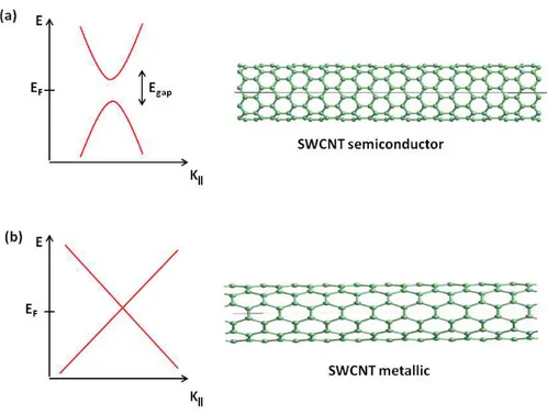
Carbon nanotubes (CNTs) can exhibit metallic or semiconducting behaviour depending on how the graphene sheet is rolled to form the cylinder of the nanotube because this modifies the band diagram of graphene (as explained in section 1.1.2). The study of the electronic features of carbon nanotubes, i.e. either semiconducting or metallic gives the ability to us to control these properties and use them for specific applications. In this section, the band structure of graphene will be explained.
1.2.1
Band Structure of Graphene
The electronic properties of graphene is related to its particular band structure. Figure 4 represents a schematic of a carbon nanotube band structure. Wallace introduced a tight-binding model for electronic band structure of graphene [4, 24]. Based on this model, the conduction $∗ and valance band $ of graphene was formulated by considering the low-energy bands of the band structure, which are approximated “as cones with apices at the K-point in the graphene Brillouin zone”[4]. The band structure of carbon nanotube is composed of two large “tent”. The conduction band, π* is above and valence band π is behind the K-point respectively [25]. The K-point is at the vertices of hexagon where the conduction band and valence band of graphene touch each other or degenerate [26]. This point is the highest equilibrium occupied state which corresponds to the Fermi energy. The Fermi level, in turn, corresponds to the zero level energy and therefore it coincides with the six points & [27] .
Figure 4
part) that intersect only at a few points (K zone. Reproduced with permission from Ref. Group.
These
graphene and of its semimetallic behaviour. The degeneracy or touching of the bands at the
bandgap which explains the metallic behaviour (zero semiconductor) of graphene
of graphene
where the electronic states are located on cones whose centres coincide with the
point, the electron has not the typical parabolic dispersion as in free space or in a material,
constant,
dispersion becomes electrons in graphene
particles like photons, for which [30, 31
electrons and holes in graphene become similar to mass
particles. In this case “electrons and holes are called Dirac fermions “ and K
11
4. Graphene electronic band structure consists of two bands (
) that intersect only at a few points (K-point) at the corners of a hexagonal Brillouin Reproduced with permission from Ref. [25]. Copyright 2007 Nature publishing
These ' points are responsible for the electronic properties of graphene and of its semimetallic behaviour. The degeneracy or touching of the bands at the K point is because of the abs
bandgap which explains the metallic behaviour (zero
semiconductor) of graphene [16, 25]. In fact, the electronic properties of graphene are related to the energy states around the Fermi level where the electronic states are located on cones whose centres coincide with the ' points [28] as shown in Figure 4. Around this point, the electron has not the typical parabolic dispersion as in free space or in a material, ( = )*+*⁄*,∗, () is the reduced Planck’s constant, + is the wavevector and ,∗ is effective mass), but the dispersion becomes ( ./)+, where ./ is the Fermi velocity of electrons in graphene [29]. This relation is similar to that of mass particles like photons, for which ( 1)+, where c is the light speed
31]. Therefore, in the band π and π*, near the electrons and holes in graphene become similar to mass
particles. In this case “electrons and holes are called Dirac fermions “ K points are often called the Dirac points [26, 31
electronic band structure consists of two bands (Upper and Lower point) at the corners of a hexagonal Brillouin . Copyright 2007 Nature publishing
points are responsible for the electronic properties of graphene and of its semimetallic behaviour. The degeneracy or point is because of the absence of a bandgap which explains the metallic behaviour (zero-band gap
. In fact, the electronic properties are related to the energy states around the Fermi level where the electronic states are located on cones whose centres hown in Figure 4. Around this point, the electron has not the typical parabolic dispersion as in free is the reduced Planck’s is effective mass), but the is the Fermi velocity of . This relation is similar to that of mass-less , where c is the light speed
π*, near the K points, the
electrons and holes in graphene become similar to mass-less quantum particles. In this case “electrons and holes are called Dirac fermions “
12
1.2.2
Metallic and Semiconducting SWCNTs
SWCNTs can exhibit metallic or semiconducting behaviour depending on the geometric structure of the SWCNT because this modifies the band diagram of graphene as discussed in section 1.2.1. The direction of rolling and the diameter of the nanotube can be obtained from the pair of integers (n, m) which identify the metallic or semiconductor type of tube. This is attributed to the quantum confinement effects when a 2D graphene sheet rolls into the 1D single walled cabon nanotube [4]. To determine the Brillouin zone inherent to the bi-dimensional unit cell of the CNT, defined by the chiral vector pointing along the circumference direction(and the translation vector T shown in Figure 5(a), the corresponding vectors of the reciprocal lattice, C* and T*, (parallel to C and T and having a length 2
|3| and |4|2 )
can be constructed [30]. The Brillouin zone of the CNT is given by the rectangle described by C* and T* [30]. When the bi-dimensional unit cell of the CNT is rolled, the electron is bound to moving in a periodic potential, with a period | |. This periodicity implies that, due to the stationary condition, the wave associated to the electron, should satisfy the following “quantization condition” [16, 25]
∙ k =2$6 or equivalently | | 76 (4) where q is a not null integer and λ is the De Broglie wavelength associated with the electron.
The quantization condition leads to a discretization of the energy levels along the circumference C, giving rise to a series of lines of quantization corresponding to the allowable values for the pairs (kx,
ky): the component of k perpendicular to the axis of the CNT, k⊥, can
take discrete values (red parallel line), while the component of k parallel to axis of the CNT, k⫽, remains a continuous variable, as shown in Figure 5(b). Therefore, the electrons are free to roam in the direction of the length of the CNT. The quantization condition can be reformulated as :/ ∗ = 6. Therefore, to stay in the first Brillouin zone it must be 0 ≤ 6 ≤ >. This means that there are N discrete values of k in the direction of the chiral vector.
Figure 5
a single sheet of graphene are arranged in a honeycomb lattice definitions of
single-walled nanotube
graphene. The valence band (which is of character)
permission from
The planes parallel to the y
quantization lines cutting the dispersion shown in
plot of the CNT. In the space of reciprocal lattice, quantization lines are spaced by an amount equal to
depending exclusively on the diameter of the nanotube
As anticipated, depending on the direction in which the graphene sheet is wrapped,
chiral
zigzag nanotube
this case, the intersections between the lines of the allowed vector
For this reason, SWCNT [32]. In particular CNT is a zig through any
13
5. “The structure of graphene and carbon nanotubes”. (a) a single sheet of graphene are arranged in a honeycomb lattice
definitions of k⊥⊥⊥⊥ and k|| (left) and a scanning tunnelling microscope image (right) of a walled nanotube”. (b), “The band structure (top) and Brillouin zone (bottom) of graphene. The valence band (which is of π-character) and the conduction band ( character) touch at six points that lie at the Fermi energy
permission from Ref. [25]. Copyright 2007 Nature publishing Group.
The planes parallel to the y-axis (energy axis) pass through the quantization lines cutting the dispersion graph of graphene in slices as shown in Figure 5(b) where (E, k⫽) are the 1D
sub-plot of the CNT. In the space of reciprocal lattice, quantization lines are spaced by an amount equal to:
∆: | | =2$ "2
depending exclusively on the diameter of the nanotube
As anticipated, depending on the direction in which the graphene sheet is wrapped, it is possible to identify CNTs of zig
type [20]. The band structure and arrangement zigzag nanotubes are shown in Figure 6(a) and 6
this case, the intersections between the lines of the allowed k and cones of the dispersion diagram in the
For this reason, SWCNTs may have different electrical characteristics In particular, if the CNT is wrapped around the y
CNT is a zig-zag type and lines of quantized wave vector do not pass through any K point and the cut does not intersect the cones apices.
. (a) “The carbon atoms in a single sheet of graphene are arranged in a honeycomb lattice”. “The insets show the microscope image (right) of a The band structure (top) and Brillouin zone (bottom) of character) and the conduction band
(π*-rgy” . Reproduced with Nature publishing Group.
axis (energy axis) pass through the graph of graphene in slices as -bands in the scatter plot of the CNT. In the space of reciprocal lattice, quantization lines
(5)
depending exclusively on the diameter of the nanotube (").
As anticipated, depending on the direction in which the graphene sheet of zig-zag, armchair or arrangement of armchair and 6(b) respectively. In this case, the intersections between the lines of the allowed wave dispersion diagram in the K points change. may have different electrical characteristics , if the CNT is wrapped around the y-axis (k⫽) the zag type and lines of quantized wave vector do not pass point and the cut does not intersect the cones apices.
Therefore, in the dispersion diagram
between the valence and conduction band and CNT will present semiconductor behaviour, Figure 6 (a).
around the x axis (:@ it is an a metallic behaviour, Figure 6
Figure 6. (a) The 1D sub-band nearest to the Fermi level does not intercept the point K1, so a band gap is formed and the CNT shows a semiconductor
band nearest to the Fermi level passes through the point K behaviour.
For chiral carbon nanotube with specific (n, m), the nanotube is metallic if n – m = 3i with
semiconductors with a band gap inversely proportional to the diameter of the nanotube [4] Therefore, 1/3 of the carbon nanotubes are predicted to be metallic, and the other 2/3 nanotubes are semiconducting.
As summary, the behaviour chirality and can be classified
a) Zigzag if A 0
14
Therefore, in the dispersion diagram of CNT, there will be a gap between the valence and conduction band and CNT will present semiconductor behaviour, Figure 6 (a). Instead, if the CNT is wrapped armchair type. In this case, CNT present
(b).
band nearest to the Fermi level does not intercept the point K1, so a band gap is formed and the CNT shows a semiconductor behaviour (b) The 1D sub-band nearest to the Fermi level passes through the point K1 and the CNT shows metallic
For chiral carbon nanotube with specific (n, m), the nanotube is m = 3i with i is an integer. [16]. All others are semiconductors with a band gap inversely proportional to the diameter Therefore, 1/3 of the carbon nanotubes are predicted to be metallic, and the other 2/3 nanotubes are
of carbon nanotubes depends on their classified into three categories:
15 b) Armchair if A 0 c) Chiral if ≠ ≠ 0
However, not any kind of CNTs is synthesized based on the rolling of graphene sheet. In fact, CNTs are grown with various chemical and physical processes. These various methods lead to carbon nanotubes having different electronic properties, different chirality and different distribution of diameters [33, 34]. Statistical studies show that each batch of carbon nonotubes contains 2/3 semiconducting and 1/3 of metallic type [35] regardless of the specifics how the carbon nanotubes are synthesized. Moreover, increasing the layer thickness of carbon nanotubes elevates the overall conductivity leading to a metallic behaviour.
1.3
Fabrication and Modelling of Devices based
on Carbon Nanotubes
In this section, the application of carbon nanotubes, particularly semiconducting single walled carbon nanotubes as an active layer for fabrication field effect transistor, will be discussed. Furthermore the use of this device for chemical/bio sensing will be also briefly explained.
1.3.1
Carbon Nanotube Electronics Device
The invention of the Field Effect Transistor (FET) in 1960 has revolutionized the life style in communication, computing, medical and digital systems. Nowadays, electronic devices are demanded to be smaller and faster. “According to Moore’s law the dimensions of individual devices in an integrated circuit have been decreased by a factor of approximately two every two years”[36, 37]. However, challenges for fabrication of small dimension transistors still remain. Therefore, in order to reduce the dimensions of transistors, while enhancing performance of the devices, another material that has improved properties at molecular scale is needed for replacement of silicon [38]. A great research activity is focused towards substitution of silicon with other materials. Among these materials, carbon nanotubes, due to their exceptional electrical properties such as high mobility at room temperature, high current density, ballistic electron
transport and nano-structure
Field effect transistor based on SWCNT has Metal-oxide-semiconductor FET (MOSFET) semiconducting SWCNTs are used as
allowing for conductivity modulation. Source (S) and drain (D) electrodes are metallic and gate electrode is forme
or top-gate [42], as shown in Figure
Figure 7. Structures of individual SWNT based field transistor (top) and a top-gate transistor
The electric current in SWCNT operation principal of FETs : the
responsible for control of the charge in the channel carriers while the horizontal electric field (drain
between the contacts imply the electric force that moves the charge carrier from one contact to the other
(BC ) modulated by gate voltage
16
[39, 40] can be an alternative choice. Field effect transistor based on SWCNT has a structure similar to semiconductor FET (MOSFET) [41]. The semiconducting SWCNTs are used as active channel material conductivity modulation. Source (S) and drain (D) metallic and gate electrode is formed either as back-gate
Figure 7 .
Structures of individual SWNT based field-effect transistors: a back-gate gate transistor (bottom)
current in SWCNT-FET is based on the fundamental the vertical electric field (gate voltage) is responsible for control of the charge in the channel by inducing charge horizontal electric field (drain-source voltage) between the contacts imply the electric force that moves the charge carrier from one contact to the other [16, 43]. Therefore, drain current modulated by gate voltage (DEF ) is quantitatively explained by
17
the transconductance (GH) as fundamental parameter of FET which correlated to the charge carrier mobility [44, 45]:
GH I DI BC EF
(6)
Via equation 6 it is possible to determine the charge carrier mobility of a transistor [46]: JKL4 DM3 CF N. GH O (7)
where M3 and O are channel length and width respectively, and N is capacitance of gate oxide.
Although single walled carbon nanotube thin film transistor (CNT-FET) and MOSFET based silicon have the same structure, the first works in accumulation mode due to the use of intrinsic semiconductor, whereas the latter operates in inversion mode due to the use of doped semiconductor [44].
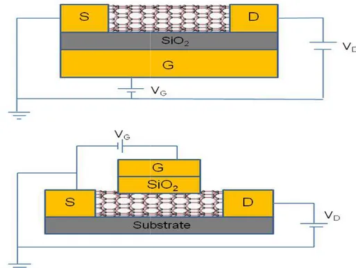
The individual nanotube transistors show high carrier mobility in the range 3,000 cm2/Vs [47, 48]. However, the assembly method of individual SWCNTs is highly challenging for technologically applicable solutions for large-scale applications. So, the complex process for making individual SWCNT-FET prevents the commercialization of this type of device [49]. Therefore, thin film based on semiconducting SWCNTs represents a promising track to scalable device manufacturing since this approach avoids the cumbersome procedure for precise control over the position of individual carbon nanotube. SWCNTs -TFT structure based on the spatial arrangement of SWCNTs in the channel of TFTs are categorized as aligned [47, 50] and random network [51-54] as illustrated in Figure 8.
Figure 8. Schematic illustration of a top Reproduced with permission from Ref. ]Copyright 2009 Nature Publishing Group Reproduced with permission from Ref and Springer-Verlag Berlin Heidelberg
Figure 8 shows a top-gate SW
random network of SWCNTs. The structure and characteristics of the bottom-gate SW
in our experiments, will be shown in Fabrication of transistors based on compared to that based on single CNT, over large area [57].
One of the most important parameter
TFT is how much percentage of semiconducting SWCNTs the active layer in the channel
generally a mixture of semiconducting and metallic
variable distribution of chiralities and diameters, resulting in heterogeneous electrical properties
nanotubes is higher than the percolation threshold obtained.
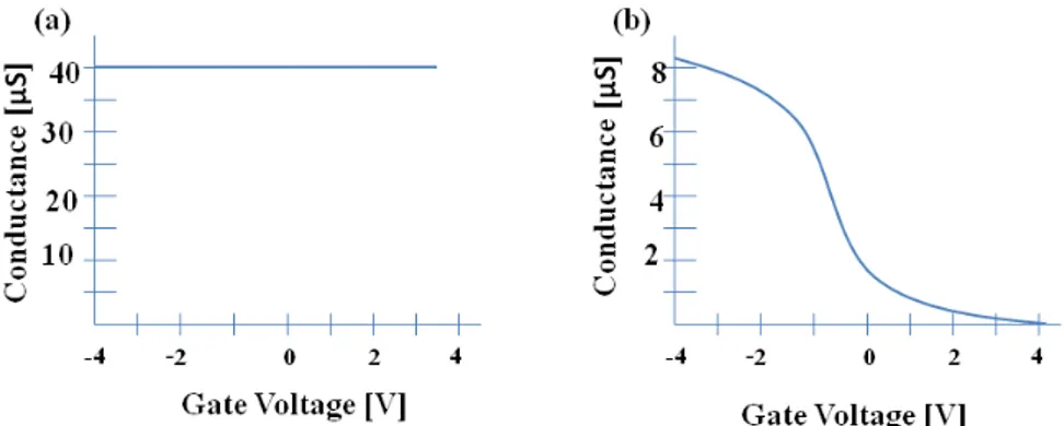
Figure 9 shows a plot of the gate voltage dependence of the conductance of either metallic or semiconducting nanotube
room temperature.
18
Schematic illustration of a top-gate SWCNT-TFT (a) aligned SWCNTs. Reproduced with permission from Ref. [55]. Reproduced with permission from Ref. [55 Nature Publishing Group. (b) random network SWCNTs [56]. Reproduced with permission from Ref [56]. Copyright 2008, Tsinghua University Press
Verlag Berlin Heidelberg.
gate SWCNTs-TFT either with aligned or SWCNTs. The structure and electronic gate SWCNTs TFT, which has been used shown in chapter 3.
based on randomized SWCNTs thin film, single CNT, has a better reproducibility parameters for fabrication of SWCNTs-uch percentage of semiconducting SWCNTs are used in
in the channel. In fact, synthesized SWCNTs are mixture of semiconducting and metallic nanotubes with variable distribution of chiralities and diameters, resulting in eneous electrical properties [58-62]. If the density of metallic nanotubes is higher than the percolation threshold, a shorted TFT is 9 shows a plot of the gate voltage dependence of the conductance of either metallic or semiconducting nanotube device at
19
Figure 9. Examples of the gate-voltage dependence of the conductance through a SWCNT at room temperature for (a) a metallic and (b) a semiconducting nanotube
Figure 9(a) shows the conductance of metallic carbon nanotube at a constant bias-voltage along it, while the gate voltage is changing. The current is independent of gate voltage [4]. On the other hand, Figure 9(b) shows the same plot for a device made from a semiconducting carbon nanotube. This device is able to be turned on and off by applying negative and positive gate voltage respectively. Moreover, the conductance changes by order of magnitude between on and off state. This is attributed to the utilization of a sufficiently high percentage of semiconducting carbon nanotubes. In fact, when there is no gate voltage, just metallic SWCNTs contribute to the current of transistor (BPQQ ) while when voltage gate is applied, the transistor turns on and a combination of semiconducting and metallic of SWCNTs are responsible for the current ( BPR). Hence, the ratio of on-current to off-on-current related to the ratio of semiconductingvs. metallic SWCNTs .
In order to profitably employ semiconducting SWCNTs, post-synthesis fabrication furnishes a reliable alternative for separating the semiconducting SWCNTs from the metallic ones. This process will be discussed in chapter 2.
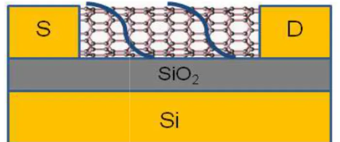
A next step for fabrication of SWCNTs-TFT is the deposition process. Researchers have developed various techniques to deposit carbon nanotube thin films on substrates. These various techniques and their detailed procedures for deposition of CNT thin film will be discussed in chapter 2, while our technique with its advantages will be discussed in chapter 3.
1.3.2
Carbon Nanotube Bio
Since the discovery of carbon nanotubes, great efforts have been done to explore this material for bio/chemical sensing
electrical characteristics and bio/chemical compatibility response of SWCNT to biomolecules is link
this material comparable to the dimension of DNA or proteins [66, 67]. Moreover
capillarity properties. The high aspect ratio) makes them one of the ideal material for and chemical components [68
m2/g) [69] of SWCNT cause more bio/chemical molecule with the carbon nanotube surf
[70].
In order to use of SWCNT as a them with electronic devices such as a transducer [48, 63]. The schematic FET for DNA detection is shown in
these sensors, compared to the traditional ones, are the possibility of obtaining selective systems, reversible and able to operate at temperature with very quick response times.
Figure 10. Schematic of DNA
The bio-sensing function is based on the bio-molecule interacts with the
electrical properties of the device instance DNAs and proteins, can SWCNTs, due to hydrophobic, and also amino-affinity of SWCNTs SWCNT thin films [73]. The mechanism
20
Nanotube Bio/chemical sensing
discovery of carbon nanotubes, great efforts have been done to explore this material for bio/chemical sensing due to the unique bio/chemical compatibility [63-65]. The response of SWCNT to biomolecules is linked to the nano-structure of this material comparable to the dimension of bio-molecules such as Moreover, the shape of SWCNT shows high aspect ratio (i.e. length to diameter ratio) makes them one of the ideal material for the adsorption of gases 68]. In addition high surface area (~ 1300 cause more bio/chemical molecules to interact carbon nanotube surface which leads to a high sensitivity In order to use of SWCNT as a biosensor, it is needed to integrate such as transistors or chemo-resistors as The schematic of a biosensor based on
SWCNT-is shown in Figure 10. The advantages of these sensors, compared to the traditional ones, are the possibility of obtaining selective systems, reversible and able to operate at room temperature with very quick response times.
Schematic of DNA-functionalized carbon nanotube biosensor
based on the conductance variation when the surface of SWCNT due to change of device [71]. Various biomolecules, for DNAs and proteins, can interact with the surface of SWCNTs, due to hydrophobic, $ S $ stacking interactions [60, 72], of SWCNTs to change the conductance of The mechanism for detection of specific
21
protein, immobilization procedure and sensitivity of thin film SWCNTs based label-free bio-sensor will be explained in detail in chapter 5.
1.3.3
Modelling of Carbon Nanotube Device
In order to improve the SWCNTs-TFTs performance, the modelling of the charge transport on the SWCNTs network inside the channel of TFT devices is an important issue to investigate. This modelling shows the relation between the physical characteristics of SWCNTs and the geometrical structure of TFTs. Several authors have studied this problem by considering a physical arrangement of the SWCNT network in a 2 dimensional (2D) model [74, 75]. Figure 11 shows the 2D simulation of nanotube network inside the channel of TFT structure.
Figure 11. (a) “Atomic force microscope (AFM) image of a CNT film where nanotubes are randomly distributed”. (b) “A 2D nanotube network generated using Monte Carlo simulations for a device. Semiconducting and metallic nanotubes are shown in light and dark color (cyan and blue color), respectively. The inset illustrates the alignment angle
TU , which defines the angle range within which nanotubes can be generated to form partially aligned CNT films in simulations”. Reprinted (Fig.1) from Ref. [75] .Copyright (2008) by the American Physical Society Publishing Group.
However, the use of a 2D model presents some limitations due to the impossibility to investigate change in the diameter of carbon nanotubes (represented as sticker rather than a cylinder). Due to the role assumed by the geometric characteristics of the SWCNT and TFT structure that affect on electrical response of a device, a 3D study of the problem by numerical simulations has been developed and it will
22
be described in chapter 4. In addition, the results obtained by simulations are compared with experimental ones to understand which parameters control the performance of device and to investigate the correlation between the percolation condition and the density of CNT network.
23
2
Chapter 2
State-of-the-art
________________________________________________________
In order to optimize the performance of electronic devices based on carbon nanotubes, researchers have investigated various ways to effectively manipulate them. There are two fundamental protocols for the assembly of thin film carbon nanotubes on substrate: 1) direct growth based on chemical vapour deposition (CVD) [76, 77]; 2) post-process deposition technique [54, 78].
This chapter is devoted to the illustration of both methods and reports the advantages of the solution deposition compared to the CVD technique. The solution deposition process not only permits the fabrication process of electronic devices at room temperature but also allows the control of electronic characteristics of either semiconducting or metallic SWCNTs. This technique is compatible for all patterning methods and it is also suitable for all kind of substrate and pre-existing circuit structures. Furthermore, various techniques for solution process deposition will be explained.
2.1
Synthesis
of
Single
Walled
Carbon
Nanotubes by Chemical Vapor Deposition
One of the most important techniques for the synthesis of carbon nanotubes is chemical vapor deposition (CVD). This method is based on directly growing of CNTs on substrate. The procedure is as follows: the solid substrate is placed in a high temperature furnace (i.e. 600 – 1000 °C) [79-81] and transition metallic catalysts such as Fe, Co, Ni [81] in nano-scale size are inserted in the furnace with ethanol or ethylene as a feedstock for converting the carbon source to form a new nucleation site for CNT growth [82]. Carbon sources, hydrocarbons [83] or carbon monoxide at high temperature are
24
decomposed and absorbed on catalysts [84] and afterward carbon nanotubes grow on the substrate. A scheme of the process is shown in Figure 12.
Figure 12. Schematic of CVD for growing CNT
The advantage of this method, compared to other methods for growing CNTs, is that by adjusting the size of catalyst and varying the temperature it is possible to control the diameter, chirality and average length of CNTs [81, 82]. However, with this method a mixture of semiconducting and metallic nanotubes is produced. Although some progress has been made to control the properties of SWCNTs during growth, none of these methods produce homogeneous electrical properties of SWCNTs batches [85]. Therefore, in order to overcome this problem, it is required to develop other methods to select features of CNTs with optimized properties for specific application [86, 87].
2.2
Single Walled Carbon Nanotubes Solution
and Preparation
As explained in section 2.1, the growth of SWCNTs on substrates with conventional CVD has to be performed in a high temperature environment, i.e. 900 °C. As a consequence, there is a limited to choice of substrates and pre-existing circuit structures [88, 89]. Moreover, electrical characteristics of grown SWCNTs are difficult to control. In fact, the synthesized SWCNTs are generally a mixture of
25
semiconducting nanotubes and metallic ones with variable distribution of chiralities and diameters, resulting in heterogeneous electrical properties [48, 58, 59, 61]. Therefore, in order to employ SWCNTs, post-synthesis deposition furnishes a reliable alternative by overcoming the high temperature problem and the expensive procedure for growing semiconducting SWCNTs. This method enables to separate semiconductive from metallic SWCNTs and it is useful for the optimal performance of devices. In order to deposit SWCNTs from solution, it is required to disperse them in an aqueous surfactant [59, 85, 90] or organic solvent [91-94] because of the inherent insolubility of them in aqueous solution. There are two main methods to disperse SWCNTs in solution: 1) chemical functionalization [95, 96] or covalent-functionalization; 2) physical interaction or non-covalent functionalization [97, 98] . In both methods, the batch of carbon nanotubes containing of mixture of metallic and semiconducting entities (also with various length and diameters) needs to be dissolved in specific solution. In the covalent process, SWCNTs are treated with strong acids and oxidants and a carboxylic acid (COOH) functionalization is produced [99]. However, the harsh conditions, alter the electronic properties of the SWCNTs [96, 100]. An alternative approach to disperse SWCNTs is the non-covalent functionalization or physical interaction. This technique disperses SWCNTs in aqueous solution preserving the electrical properties of SWCNTs.
Generally, grown carbon nanotubes are in bundle form due to the strong Van der Waals interaction [101] and hence it is needed to de-bundle and suspend them in aqueous solution. Moreover, carbon nanotubes are a non-polar material and have a hydrophobic surface [6] and they are not dissolvable in water. Hence, in order to increase their solubility it is needed to attach amphiphilic surfactants to their surface [102]. The amphiphilic surfactants have a hydrophobic tail and hydrophilic head [6]. The hydrophobic tail interacts with hydrophobic surface of SWCNT via hydrophobic/hydrophobic interaction, while hydrophilic head facilitates the dispersion in aqueous solution [97]. The wrapping of the surfactants around the SWCNTs is shown in Figure 13. Then, by the help of sonication the Van der Waals forces between tubes are overcome and the conversion of the bundle to the individual SWCNTs takes place [102, 103]. The surfactants, in fact, deposit on the surface of SWCNTs and being charged, introduce
electrostatic repulsion and stabilize solution [96].
Figure 13. Schematic illustration of various surfactant assembly structures on a SWCNT, including (a) cylindrical micelles, side and cross
and (c) random adsorption
After that, the centrifugation of the solution separates the SWCNTs from amorphous carbon and remove large bundle that still remain in solution [85].
surfactants able to disperse
solutions are: sodium dodecyl sulfate (SDS) dodecylbenzenesulfonate (SDBS)
109].
Recently, by using density gradient ultracentrifugation (DGU) separation of semiconducting SWCNTs from metallic ones as reported in Figure 14 [85], has been achieved. In this cond
smaller-diameter semiconducting SWCNTs are found on the top layer of the vial. On the other hand, high density metallic SWCNTs settle at the bottom of the vial. As it can be seen from
different bands verify the sort
as identified by UV-Vis spectroscopy
26
electrostatic repulsion and stabilize the isolated single CNTs in
Schematic illustration of various surfactant assembly structures on a including (a) cylindrical micelles, side and cross-section views, (b) hemimicelle,
After that, the centrifugation of the solution separates the SWCNTs from amorphous carbon and remove large bundle that still remain in surfactants able to disperse Successfully SWCNTs in aqueous sodium dodecyl sulfate (SDS)[104, 105], sodium dodecylbenzenesulfonate (SDBS) [106, 107], and Triton X [108, Recently, by using density gradient ultracentrifugation (DGU) the semiconducting SWCNTs from metallic ones as reported , has been achieved. In this condition, low density diameter semiconducting SWCNTs are found on the top layer of the vial. On the other hand, high density metallic SWCNTs settle at As it can be seen from Figure 14, observed the sorting of SWCNTs based on their diameter Vis spectroscopy [85].
27
Figure 14. Sorting SWNTs using density gradient ultracentrifugation (DGU ). a, Small-diameter (0.7–1.1 nm) SWNTs encapsulated with sodium cholate are sorted by Small-diameter following DGU. b, Optical absorbance spectra for different fractions, further confirm sorting by diameter. c, Large-diameter SWNTs are sorted according to electronic type following DGU. Reproduced with permission from Ref. [85]. Copyright 2008 Nature Publishing Group
2.3
Deposition Methods for SWCNTs Solution
The assembly of SWCNTs from solution provides a strategy for construction of a thin film on a substrate that is technologically applicable for large areas and gives the possibility for fabrication of electronic devices at room temperature. Various methods for deposition SWCNTs in solution for assembly thin film have been demonstrated such as spray coating [88], dip coating [65], spin coating [90], dielectrophoresis deposition [89], and electrophoretic deposition [110]. This section will report these techniques.
2.3.1
Spray Coating
One of the techniques to form SWCNTs thin film from solution is spray-coating. The schematic of
Figure 15. The system is based on main parts for control the process and drying process [111]. The mechanism for inserting SWCNTs solution
aerosol from the solution 3) atomizer control
for transporting the droplet from nozzle to destination substrate by controlling gas flux and position of pistol.
Figure 15. Schematic of spray-coating
M. Jeong et al. utilized spray thin film from solution on substrate
order to enhance the deposition, they used aminopropyltriethoxysilane (APTES)
and sprayed the solution on the top of the hot plate at 100 °C in order to accelerate the evaporation of the solvent. Although this method is simple and allows the control of the thick
repeating the process, however
needed for coating, it is not suitable for particularly for flexible substrate
2.3.2
Dip Coating
Another method to create a thin
coating. In this method, a substrate is immersed and pulled up in bath
28
One of the techniques to form SWCNTs thin film from solution is The schematic of a spray coating system is shown in is based on a pistol which is composed of three for control the process and a hot plate for acceleration mechanism is as follows: 1) Vessel is used solution, 2) atomizer is utilized to form an atomizer control the injection of solution for transporting the droplet from nozzle to destination substrate by
and position of pistol.
coating
utilized spray-coating deposition to form SWCNTs bstrate for transistor fabrication [112]. In order to enhance the deposition, they used 3-aminopropyltriethoxysilane (APTES) for silanization of the substrate
the solution on the top of the hot plate at 100 °C in order to accelerate the evaporation of the solvent. Although this method is simple and allows the control of the thickness of the thin film by however, due to the relatively high temperature is not suitable for thermally sensitive substrates, particularly for flexible substrates..
thin film of SWCNTs from solution is dip-coating. In this method, a substrate is immersed and pulled up in bath
29
solution with specific speed and continuously depending on the desired thickness of thin film [113, 114] . A schematic of the process is shown in Figure 16.
Figure 16. Schematic of deposition dip-coating. Reproduced with permission from Ref. [114]. Copyright 2009 IOP Publishing Group
X. Xiong et al. applied dip-coating method with photolithography for selective assembly of SWCNTs network on the polymer substrate (parylen-C) [114]. This process is based on a difference in surface energy. The micro-trenches which were patterned by using optical lithography have a hydrophobic surface and SWCNTs were not absorbed on its surface. Therefore, it is needed to modify the surface to become hydrophilic. In this case, the surface become hydrophilic by utilizing O2 plasma treatment and thus SWCNTs were attracted on the
modified hydrophilic surface. This method allows the SWCNTs selectivity deposited on hydrophilic surface on the micro-trenches by dip-coating method. This method is quite simple and cost-effective. However, this process not only need a special instrument to control the deposition process and is difficult to handle process, but also the surfactant-wrapped SWCNTs can degrade the electronic properties of device.
2.3.3
Spin Coating
Spin-coating is a process for assembly of thin films on a flat substrate. A specific amount of solution is dispensed on the substrate while rotating at specific speed. Therefore, the solution spreads on the
substrate by shear forces [100
evaporates and the SWCNTs remain on the substrate. spin-coating is shown in Figure
Figure 17. Spin-coating process. Used in part
from Ref. [116]. Copyright 2004 American Chemical Society.
LeMieux et al. have used spin
SWCNTs in the fabrication of transistor
technique [117]. In order to overcome hydrophobic surface of SWCNTs for enhancing attachment on
types of silanes with amino and phenyl groups functionalization. The amino
semiconducting SWCNTs to be
terminated surface leads to the attachment of same authors showed later
SWCNTs solution and rotation
SWCNTs can be aligned in the channel of TFT structures.
However, the spin coating approach for the deposition of SWCNTs is suitable for device arrangement compatible with the dimension of the rotating equipment and therefore limited to
2.3.4
Dielectrophoresis Deposition
Another method for assembling SWCNTs t dielectrophoresis. In this method,
30
100, 115]. In this manner, the solvent he SWCNTs remain on the substrate. A schematic of
Figure 17.
Used in part of this figure is Reprinted with permission American Chemical Society.
spin-coating for assembly of thin films of fabrication of transistor based on the self sorted . In order to overcome hydrophobic surface of SWCNTs for enhancing attachment on the substrate, they used two s with amino and phenyl groups for the substrate The amino-terminated surface causes more to be attracted on it while phenyl-the attachment of more metallic ones. The
that, by controlling the volume of and rotational speed of the spin coating device, the aligned in the channel of TFT structures. [118]. spin coating approach for the deposition of SWCNTs is suitable for device arrangement compatible with the dimension of the rotating equipment and therefore limited to small scale arrays.
Dielectrophoresis Deposition
Another method for assembling SWCNTs thin films is this method, carbon nanotubes become polarized
under electrodes Figure
frequency and voltage on the
Figure 18
There are various parameters
of electric field, electric permittivity of solution and SWCNTs particles
transistor
carbon nanotubes on solution
leads to align the electrode
semiconducting ones.
2.3.5
Electrophoresis is another kind of deposition of SWCNTs solution on the desired substrate. The
solution is placed between
31
under an anisotropic electric field which align
electrodes [119-121]. The schematic for dielectrophoresis is shown in Figure 18. By applying an alternating electric field with
frequency and voltage allows to align SWCNTs by inducing a the SWCNT particles in the solution. [122, 123]
18. Schematic arrangement for dielectrophoresis-based alignment of CNTs
There are various parameters affecting this process of electric field, electric permittivity of solution and
SWCNTs particles [120]. J. Li et al. have fabricated field effect transistors based on this method and have controlled the number of carbon nanotubes on the basis of concentration
solution and deposition time. Although dielectrophoresis approach leads to align the carbon nanotubes in channel (between
electrodes), it acts more effectively on the metallic nanotubes semiconducting ones.
Electrophoretic Deposition
Electrophoresis is another kind of deposition of SWCNTs solution on the desired substrate. The procedure is as follows:
solution is placed between two electrodes subjected to an electric them between two dielectrophoresis is shown in electric field with specific allows to align SWCNTs by inducing a dipole
].
based alignment of CNTs
this process including strength of electric field, electric permittivity of solution and the properties of abricated field effect olled the number of concentration of SWCNTs in dielectrophoresis approach nanotubes in channel (between the two etallic nanotubes than on
Electrophoresis is another kind of deposition of SWCNTs solution on as follows: the SWCNTs two electrodes subjected to an electric
32
field. The SWCNT particles become polarized under the non-uniform electric field and are attracted towards the electrodes. Accumulated SWCNTs on the electrode are collected from the electrode and used for formation of a thin film [82]. The schematic of the electrophoresis process is represented in Figure 19.
Figure 19. Schematic of electrophoresis deposition
Lima et al. formed thin film carbon nanotubes on a non-conductive substrate for making a transparent conductive electrode [110]. Although this method is simple and quick, it is not technologically applicable for large areas of deposition and it is not able to remove the surfactant from SWCNTs.
33
3
Chapter 3
Experimental Process for
Fabrication of SWCNTs-TFT
________________________________________________________
In this chapter the fabrication of thin film transistors (TFTs) based on high purity semiconducting SWCNTs will be described. In the first part, the procedures for dispersing SWCNTs in the surfactant solution will be explained. Afterwards, our effective method, which is a combination of substrate silanization and vacuum filtration method, will be illustrated. Then, the electrical characterization of SWCNTs-TFTs will be presented. Moreover, the advantages of this technique will be discussed.
The schematic of back-gate SWCNTs-TFT is shown in Figure 20.
Figure 20. Schematic of SWCNTs-TFT
All the SWCNTs-TFT structures were fabricated and measured at room temperature. The electrode configuration, explained in subsection 3.1.1 followed by a deposition procedure reported in subsection 3.1.2 and 3.1.3, is chosen in order to create the active layer of the structure.
3.1
Dispersion
Process
SWCNTs on Aqueous
The 90% semiconducting SWCNTs powder synthesized by CoMoCAT®-CVD method
(SWeNT® SG-65) [124]. The average diameter of SWCNTs in the powder form is between 0.7-0.9 nm
was dispersed in surfactant based was sodium dodecyl benzene sulphonat C12H25C6H4SO3Na). This ionic
improve the dispersion of SWCNTs in
schematic of the interaction between SDBS and shown in Figure 21.
Figure 21. Schematic representation of
The procedure for dispersing of SWCNTs in follows: 0.05 mg of SWCNTs were
aqueous solution (deionized water sedimented in the bottom of vial. overcome Van der Waals force individual separated CNTs , the ultrasonic bath. In order to prevent the
34
Dispersion
Process
of
Semiconducting
queous Solution
The 90% semiconducting SWCNTs powder synthesized by is obtained from sigma-Aldrich Co. The average diameter of SWCNTs in the 0.9 nm with chirality (6,5). The powder surfactant based aqueous solution. The surfactant l benzene sulphonate (SDBS, chemical formula ionic surfactant was chosen in order to SWCNTs in the aqueous solution [125]. The e interaction between SDBS and SWCNTs surface is
Schematic representation of SDBS and its interaction with SWCNT surface
The procedure for dispersing of SWCNTs in aqueous solution is as 0.05 mg of SWCNTs were added to 1 wt% of SDBS in (deionized water, 10 mL). The SWCNTs powder in the bottom of vial. In order to disperse them well, i.e. to overcome Van der Waals forces for converting bundle form to
, the vial was sonicated for 3 hours in In order to prevent the solution from over-heating, ice
![Figure 8. Schematic illustration of a top Reproduced with permission from Ref. ]Copyright 2009 Nature Publishing Group Reproduced with permission from Ref and Springer-Verlag Berlin Heidelberg](https://thumb-eu.123doks.com/thumbv2/123dokorg/7213140.76655/24.892.119.523.252.455/schematic-illustration-reproduced-permission-copyright-publishing-reproduced-heidelberg.webp)


![Figure 15. The system is based on main parts for control the process and drying process [111]](https://thumb-eu.123doks.com/thumbv2/123dokorg/7213140.76655/34.892.159.520.540.705/figure-based-main-parts-control-process-drying-process.webp)
