ALMA MATER STUDIORUM - UNIVERSITÀ DI BOLOGNA
SCUOLA DI INGEGNERIA E ARCHITETTURA
DIPARTIMENTO DI INGEGNERIA DELL’ENERGIA ELETTRICA E DELL’INFORMAZIONE G. MARCONI
CORSO DI LAUREA MAGISTALE IN INGEGNERIA ENERGETICA
TESI DI LAUREA MAGISTRALE In
Tecnologie Innovative per la Produzione, il Trasporto e l'Accumulo dell'Energia Elettrica M
Surface Plasmon Induced Luminescence as a Tool for Study of
the Ageing of Polymeric Materials
CANDIDATO RELATORE:
Luca Montanari Prof. Ing. Davide Fabiani
CORRELATORI: Dr. Gilbert Teyssedre Dr. Kremena Makasheva Dr. Christian Laurent Anno Accademico 2015/16 Sessione III
1
Table of Contents
Chapter 1 State of the Art
... 51.1 Insulating polymers and electrical applications ... 5
1.1.1 Polymeric materials: from insulators to conductors ... 5
1.1.2 A Brief History of Development in Electrical Insulation ... 7
a) From oil impregnated paper to Polyethylene ... 7
b) Composites and nanocomposites ... 9
1.2 Reliability of insulating materials ... 10
1.2.1 Key properties of insulating materials ... 10
1.2.2 Space charge as a threat in insulating polymers ... 11
1.2.3 Ageing Diagnosis ... 12
1.3 Luminescence processes in insulating polymers ... 13
1.3.1 Introduction ... 13
1.3.2 Photoluminescence – optical excitation ... 15
a) Fluorescence ... 15
b) Phosphorescence ... 16
1.3.3 Electroluminescence ... 17
a) Electroluminescence mechanism in dielectric materials ... 18
b) Relaxation process and possible luminescent centres ... 19
c) Electroluminescence and electrical ageing ... 20
1.4 Surface Plasmons ... 22
1.4.1 Introduction ... 22
1.4.2 Coupling surface plasmons and photons: conditions for radiate relaxation ... 23
1.4.3 Spectral distribution of the light emitted by SP ... 24
1.4.4 SP implication in electroluminescence spectra ... 25
1.4.5 Silver nanoparticles (AgNPs) as the most appropriate nanostructures to support surface plasmons... 26
1.5 Purpose of the thesis ... 29
1.6 Plasma deposition techniques for synthesis of AgNPs in silica-like matrix ... 32
2
1.6.1 Introduction ... 32
1.6.2 Plasma Enhanced Chemical Vapor Deposition (PECVD) ... 33
Chapter 2 Experimental Materials and Techniques
... 352.1 Materials (Polypropylene) ... 35
2.2 Experimental setups ... 36
2.2.1 Sample preparation ... 37
a) Gold metallization setup ... 37
b) ITO sputtering setup ... 37
c) Treatment of electrode edges ... 38
2.2.2 Luminescence setup ... 39
a) Excitation source ... 40
b) The photomultiplier detector – photons counting ... 44
c) The monochromator and CCD camera – spectra acquisition ... 44
2.2.3 Plasma reactor description ... 45
2.2.4 Monitoring of the plasma process by OES ... 49
2.2.5 Ellipsometry ... 50
Chapter 3 Experimental results
... 53Synopsis ... 53
3.1 EL from reference structures ... 53
3.1.1 Samples ... 53
3.1.2 Protocols ... 55
3.1.3 Field dependence of EL under AC stress ... 59
3.1.4 Phase resolved EL under AC stress ... 62
3.1.5 Discussion ... 68
3.2 AgNPs tailored BOPP: structure and EL characterisation ... 72
3.2.1 Sample preparation ... 73
3.2.2 Physico-chemical characterization of the composite layer ... 75
3.2.3 Field dependence of EL under AC stress ... 78
3.2.4 Spectral analyses ... 84
3.2.5 Discussion ... 86
3.3 Conclusion and Perspective ... 89
5
Chapter 1 State of the Art
1.1 Insulating polymers and electrical applications
Polymers are frequently found in our surroundings from personal computers to car manufacturing, from living facilities to military installations. More specifically, some insulating polymers are widely used with their electrical insulating properties to electrical engineering applications.
The term polymer has been used since the early 1830s and was first coined by Jons Jakob Berzelius [1]. However, a true understanding was not attained until the 1920s and, since then, some of the most famous polymers have been developed, such as – Nylon, polyethylene, Teflon and silicones [2].
A polymer is composed of a long chain of repeated units, called monomers. The most common technological polymers are plastics, issued from petroleum industry, however there are other forms such as cellulose, a naturally occurring polymer found in plants Engineering plastics can be created from a single polymer, or by adding a second phase, e.g. an inorganic materials to form a composite. In this way it is possible to enhance key properties to render the base polymer more suitable for use in a particular application.
Specially, polymers have a very important role as insulating media because of their electrical and thermal properties. Furthermore polymers are usually easy to produce and they have a low effective cost. Polymers are often manufactured for strengthened properties, for example, cross linked Polyethylene (XLPE) is produced to achieve higher dielectric strength and thermomechanical stability.
1.1.1 Polymeric materials: from insulators to conductors
Typical requirements for an electrical insulator are: it must have a high enough dielectric strength to withstand an electrical field between the conductors; it must have a high electrical resistivity to prevent leakage of current across the conductors. It must possess a good resistance to discharges to prevent damage in case of arcing. Insulating materials must be mechanically strong to resist shocks,
6
vibrations, and other mechanical forces. It must maintain integrity under a wide variety of environmental hazards (e.g., humidity, temperature, and radiation) [3]. To describe electrical properties of polymers means to thoroughly examine their responses to the electric field applied to them. Unlike metals, which respond readily to an electric field by electronic conduction, the response of polymers is more complex.
In general, the electric conduction in polymers is very low, which makes them useful as very effective electric insulators. If there is any conduction in a polymeric substance, it is often caused by impurities that provide tiny charge carriers in the form of electrons and/or ions. They provide very good insulation solutions but are subjected to deterioration in service under the influence of electrical, thermal stress and other degradative stresses. In addition, at sufficiently high fields, when the applied voltage exceeds a certain value, a variety of processes will cause a complete breakdown of the polymeric material serving as insulation. Their use in practical applications is for that reason limited.
The electric breakdown must be prevented, because it leads to failure of an electric component or may endanger people handling the component. Some materials are designed to work as safe insulators under low or moderate voltages, while some are developed to be used under high or extra-high voltages (HV or EHV).
High-voltage direct current (HVDC) applications are nowadays increasing and polyethylene-based materials are thermoplastic materials widely applied for HVDC cables insulation.
On the other hand there still exist some conductive or semi-conductive polymers which have a narrow band gap.
Conductive polymers, more precisely, intrinsically conducting polymers, such as polyacetylene (its high electrical conductivity was discovered in the 1970s [4] and recognized by the Nobel Prize in Chemistry in 2000) and phenylene vinylene (PPV, a famous family of semiconducting polymers and extensively used in organic light emitting diodes), are organic polymers that conduct electricity. They can have metallic conductivity or can be semiconductors. Most of the conductive polymers are not pure polymers but compounds, while even polymers themselves are not pure at all because of their degrees of polymerization and catalyst residues and impurities introduced during the manufacturing process. Their electrical and
7
photo-physical properties can be fine-tuned using the methods of organic synthesis and advanced dispersion techniques. Conductive polymers or conjugated polymers have drawn attention of scientists and encouraged the rapid growth of this field. Since the late 1980s, organic light emitting diodes (OLEDs) and organic photovoltaic cells have emerged as important applications of semiconducting polymers [5]. Consequently, the electroluminescence features in materials for OLEDs has been investigated extensively and deeply [6].
In general, in OLEDs there are still two basic problems or challenges: the “luminescent efficiency” and “stability” of materials and devices. The “luminescent efficiency” can be improved by specially designed structure such as electron or hole injection layers and transport layers, or by special materials such as using phosphorescent materials to replace fluorescent materials with higher luminescent efficiency. The “stability” or in another words “electrical ageing” is also a basic issue for insulating polymers in electrical applications. The ageing mechanism of semiconducting polymers and insulating polymers can be merited from each other.
1.1.2 A Brief History of Development in Electrical
Insulation
a) From oil impregnated paper to Polyethylene
The development of electrical insulating polymeric materials is closely associated with the development of electrical apparatus [7]. In this paragraph I will briefly present an historical overview about the materials used as electrical insulator all the way up to the modern insulating polymers.
After Edison (and General Electric) lost the fight with Westinghouse and AC triumphed over DC in the early 1900's as the most appropriate form to transport electricity, it was necessary to develop electrical insulation for much higher voltages. Carefully dried paper impregnated with mineral oil was used for transformers in steel tanks and capacitors in cans at increasingly higher voltages. By 1925 oil impregnated paper, sheathed with lead, was used generally for underground cable at 13.8 kV and even up to 69 kV [8].
8
Many of the natural materials were extensively modified to improve their insulating characteristics. Special papers for transformers and capacitors were developed along with mineral oils selected for each application. So even before the introduction of synthetic materials a fairly wide variety of specialized, relatively inexpensive, insulating materials had been developed.
In about 1925 alkyd (saturated polyester) resins followed the somewhat earlier introduction of phenolic resins (Bakelite), as the first synthetic insulating materials. Improved heat and oil resistance won acceptance for these materials in insulating varnishes.
In 1930s poly(vinyl chloride) (PVC) was introduced to replace natural rubber in underground cable and house wiring. Resistance to fire, solvents and oil were advantageous but a low softening temperature, poor resistance to heat aging (oxidation and loss of plasticizer) and high electrical loss compared to rubber limited its application.
In about 1963 extruded polyethylene (PE) began to replace a great deal of lead jacketed, oil impregnated paper for 13 and 23 kV underground, residential distribution (URD) cable.
Failures in buried PE cable started to occur after about five years in service and were found to accelerate as time passed. At first the cause of the failures was a mystery. Voltage "treeing" was a recognized mechanism for voltage failure, but examination found an unrelated and previously unrecognized failure mechanism - "water" treeing. Over 1000 papers have now been published on water treeing and the phenomena involved still are only partly understood.
Cross-linked polyethylene (XLPE) was introduced about two years after the first use of high density PE, this is the early days of modern synthetic polymeric insulation.
From 1980s to 1990s, appeared some new concepts in high-field phenomena, such as band theory for describing the electronic properties of partially crystalline materials and field-limiting space charge for describing conduction in polyolefins. It was also the dawn of space charge measurement, i.e., the direct measurement of internal charge density distribution in bulk insulation. Several techniques such as laser-induced pressure pulse method and pulsed electroacoustic method were introduced.
9
From 1990s to 2000s, polymeric insulation dedicated to HVDC applications appeared as new need. The insulating materials for HVDC cables, such as XLPE, were investigated deeply.
From 2000s to present, came the nano age [7]. The booming of study on nanocomposite materials clearly marks the decade. In addition, lessons learned from space charge measurements, e.g. the bipolar nature of transport and significant injection of electronic carriers, and from electroluminescence measurements, e.g. charge recombination, have been used in an attempt to provide a complete description of insulating polymers.
b) Composites and nanocomposites
Engineering plastics can be created from a single polymer, or by adding a second phase, e.g. an inorganic mineral, to form a composite. In this way it is possible to enhance key properties to render the base polymer more suitable for use in a particular application. For example Haque et. al. [9] investigated mechanical and thermal properties of glass/epoxy nanocomposites with added nanoclays such as MMT. They found significant improvements in mechanical properties with addition of 1% organo silicate nanoparticles.
While polymer composites have a long history, a critical advance in the subject occurred in the early 1990s when research at Toyota showed the benefits that can result from reducing the size of the included mineral phase. This work led to the concept of a nanocomposite, interest in which has increased at a rapid rate ever since.
In the last two decades, the design of composite materials comprising either micro-scaled or nano-scaled inorganic particles has gained increased attention in power and high-voltage engineering. Particularly, the use of micro- and nanotechnologies offers new approaches towards improved insulation systems that operate at higher temperatures and electrical stress.
Composite materials typically consist of two or more components that comprise significantly different physical and/or chemical properties. Due to the controlled combination of the components, new materials are obtained with distinct properties from the individual components [10]. If at least one of the components has nanometric dimensions, these materials are termed nanocomposites.
10
In the power industry, inorganic fillers particularly aluminum nitride (AlN), boron nitride (BN), silicon dioxide or silica (SiO2), aluminum oxide or alumina (Al2O3),
titanium oxide or titania (TiO2), silicon carbide (SiC) and zinc oxide (ZnO), etc. are
usually incorporated into electrical insulating polymers to achieve specific electrical, mechanical, and thermal properties [11].
1.2 Reliability of insulating materials
1.2.1 Key properties of insulating materials
With the materials improvement, intrinsic limits are being approached for understanding high field effect in insulators.
The resistance of nanocomposites to partial discharges and electric treeing enables the design of new insulation systems with enhanced electrical breakdown strength. Besides electrical properties, mechanical strength as well as thermal conductivity plays an important role in selected applications such as insulation systems of large electrical machines. In addition, permittivity and dissipation factor are desired to be as low as possible for electrical insulation whilst for capacitors, loss factor should be as high as possible. Flame retardancy is a property desired for cables insulation used in the radiation field in tunnels, while tracking resistance is very important for outdoor insulators [12].
Withstanding electrical stresses remains one of the greatest concerns for materials in electrical engineering and researches address different items, link to materials and process quality, physical understanding of processes, and design of new materials.
The greatest sources of failures are related to the presence of impurities, protrusions and voids within the polymer resulting in locally enhanced electrical stresses, which can lead to initiation of partial discharges (PD) or growth of electrical trees within the insulation [1]. All these things are known and progress in the reliability of systems has been reached by quality improvement. As now we supposedly come closer to intrinsic limit of materials, the focus in research is more on the understanding of ageing processes.
11
The role played by electrostatic charges, through electrostatic and electrodynamic effects is currently under the focus. Electrical charges modify the internal field distribution, leading to a critical enhancement upon voltage polarity reversal (cf. DC case below). It is also at the origin of a local material degradation upon charge recombination or hot carries effects. Through cumulative effects, it can generate large defects initiating PDs and leading to the ageing scheme explained above. Whichever the mechanism by which this ageing process occurs, it is of particular interest to understand the earlier causes of changes for the purpose of improving lifetime prediction and condition monitoring techniques.
Composites participate to strengthening materials against electrical stresses. Inorganic particles notably harden materials against the action of surface discharges. Among properties enhancement, one of the most promising with composites is the change in electric strength that has been reported when the filler particles attain nanometric dimensions.
1.2.2 Space charge as a threat in insulating polymers
Electrical charging of insulating polymers, used as bulk insulation in high voltage equipment, represents a major drawback and must be avoided especially in high voltage direct current (HVDC) applications. Space charge in polyethylene-based materials still constitutes a problem affecting reliability of HVDC lines. Understanding space charge in insulating polymers has been the subject of a strong activity in the international community within the last 30 years.
Charging in these materials can occur by internal generation or by charge injection at the electrode/polymer contact. Internal generation can be linked to numerous reactions occurring under thermal/electrical stress owing to complex chemical formulation of the material with additives, such as anti-oxidants, residues, and impurities.
The accumulation of electrical charges forming internal space charge under HVDC conditions has two major consequences: (i) the internal electric field distribution is not anymore the design field. It represents a risk of formation of local domains where the higher fields values can initiate current runaway of thermal or electrical origins eventually leading to electrical breakdown [13, 14], and (ii) by cumulated
12
local damages to the structure of the dielectric at a molecular level. Local defects can be extended up to the stage where electrical discharges and electrical treeing can appear leading ultimately to breakdown. [15,16,17].
All these events induce a loss of system reliability. Being part of larger power systems, a local breakdown in one of the system constituents can give rise to much larger consequences (blackout of a large grid for example).
Preventing the formation of space charge in insulation is therefore a necessary step to enhance system reliability, allowing a higher level of integration of power system with the associated gain in terms of environment and space saving.
The main route followed for avoiding space charges in insulations is that consisting in improving crosslinked polyethylene regarding the amount of residues: crosslinking is known to produce polar by-products that detrimental to the DC performances by producing copious charge generation. Another way we have followed is that consisting in limiting electronic carriers generations.
Recently, a very efficient method to block charge injection was developed by inserting a nanocomposite layer between the semi-conducting electrode and the polymer: the idea consists of deposition of a semi-insulating nanoscale layer with metallic inclusions. The layer is composed of a single plane of silver nanoparticles (AgNPs) embedded in a semi-insulating organosilicon matrix deposited on the polyethylene surface by a plasma process. Control over size, density and surface coverage of the nanoparticles is achieved through the plasma process operating parameters. A drastic effect was observed and attributed to the presence of AgNPs acting as artificial deep traps for injected charges which prevent from charge injection in the polymer [18,19, 20].
1.2.3 Ageing Diagnosis
Measurements of electrical properties useful for insulation characterization and for aging diagnosis were carried out by different research groups in the framework of the European project “ARTEMIS” (Aging and Reliability Testing and Monitoring of Power Cables: Diagnosis for Insulation Systems), with the aim to investigate the degradation mechanisms and to evaluate reliability of high voltage cross-linked polyethylene (XLPE) cables. Among these properties, space charge,
13
charging/discharging current, polarization loss and electroluminescence (EL) measurements are associated with the mechanism of charge injection and transport [21].
There is a general agreement among researchers that electrical aging of synthetic insulation used in high voltage cables could be started by space charge accumulation.
Electroluminescence emission enables a link to be made between space charge phenomenology and the release of energy due, for example, to radiative charge recombination. It is therefore of importance to be able to define levels of fields and associated space charge profiles that are liable to give rise to luminescence excitation since EL is the evidence of the existence of highly reactive excited states in the insulation that could promote accelerated aging [22].
In the next section we will introduce the phenomenon of luminescence, with particular attention to the electroluminescence in insulating polymers. Specifically we will analyse how the measurement of this feature can reveal some important detail of the materials.
1.3 Luminescence
processes
in
insulating
polymers
1.3.1 Introduction
Luminescence is an old technique. It’s fully described for the first time by Sir G.G. Stokes who reported the theoretical basis for the mechanism of absorption (excitation) and emission. Today luminescence, in its varied forms, is one of the fastest growing and most useful analytical techniques in science. Applications can be found in areas as diverse as materials science, environmental science, microelectronics, physics, chemistry, biology, biochemistry, medicine, toxicology, pharmaceuticals, and clinical chemistry. This rapid growth has occurred only in the past couple of decades and has been principally driven by unique needs of the life sciences.
14
Luminescence techniques are nowadays more and more utilized because of their important advantages:
High sensitivity, for highly luminescent compounds, concentrations as low as the one part per billion to one part per trillion can be detected. This is a sensitivity approximately 10,000 times greater that absorption spectroscopy.
Good selectivity, specificity in luminescence arises from two factors, only about 10% of all substances that absorb radiation re-emit it as light and there are two selectable wavelengths (excitation and emission) in luminescence as opposed to only one in absorbance. It is highly unlikely that two substances will share both a similar excitation and emission. This is because the difference between excitation and emission peaks can range anywhere from several nanometers to hundreds of nanometers (UV to infrared).
Environmental qualitative information, Because of the longer lifetimes involved in the electronic transitions of luminescence, it is far more sensitive to the local environment than absorbance.
In accordance with various excitation sources, there are several methods allowing the productions of luminescence from dielectrics:
1. Photoluminescence (PL), including Fluorescence and Phosphorescence (also called UV induced luminescence);
2. Electroluminescence (EL), Mixture of excitation processes induced by electric field;
3. Cathodoluminescence (CL), induced by an electron beam;
4. Charge Recombination induced Luminescence (RL), recombination between trapped carriers, no kinetic energy;
5. Chemiluminescence (CHL), derives its energy from chemical reactions. It is the breaking of chemical bonds that supplies the energy;
6. Triboluminescence, is derived from the Greek word tribo meaning to rub. It is emitted when certain materials are stressed, crushed, or broken;
7. Thermoluminescence as luminescence following sensitization through e.g. ionizing radiation followed by heating inducing charge detrapping and recombination
15
1.3.2 Photoluminescence – optical excitation
Photoluminescence is light emission from materials after the absorption of photons (electromagnetic radiation). Photoluminescence is further divided into categories: fluorescence and phosphorescence. Today they are defined via the emission based on quantum mechanical mechanism for the orbital angular momentum multiplicity of the emitted electron (i.e. the singlet or triplet excited states). However, before the advent of quantum theory photoluminescence was defined on the basis of empirical evaluation of the duration of emission lifetime. The process can be described as: the material absorbs photons, to be excited to states at high energy level, then release back to the ground state, meanwhile emitting light. The emitted light has a lower energy and therefore longer wavelength than the excitation light.
a)
FluorescenceFigure 1 - 1: representation of Fluorescence stages.
Stage 1: Excitation
A photon of energy ℎ is supplied by an external source such as an incandescent lamp or a laser and absorbed by the fluorophore, creating an excited electronic singlet state (S1'), cf. Fig. 1-1.
16
The excited state exists for a finite time (typically 1-10 nanoseconds). During this time, the fluorophore undergoes conformational changes and is also subject to a multitude of possible interactions with its molecular environment. These processes have two important consequences. First, the energy of S1' is partially dissipated, yielding a relaxed singlet excited state (S1) from which fluorescence emission originates. Second, not all the molecules initially excited by absorption (Stage 1) return to the ground state (S0) by fluorescence emission. Other processes such as collisional quenching, fluorescence resonance, energy transfer and intersystem crossing may also depopulate S1. The fluorescence quantum yield, which is the ratio of the number of fluorescence photons emitted (Stage 3) to the number of photons absorbed (Stage 1), is a measure of the relative extent to which these processes occur.
Stage 3: Fluorescence Emission
A photon of energy ℎ is emitted, returning the fluorophore to its ground state S0. Due to energy dissipation during the excited-state lifetime, the energy of this photon is lower, and therefore of longer wavelength, than the excitation photon ℎ . The difference in energy or wavelength represented by (ℎ – ℎ ) is called the Stokes shift. The Stokes shift is fundamental to the sensitivity of fluorescence techniques because it allows photons emission to be detected against a low background, isolated from excitation photons. In contrast, absorption spectrophotometry requires measurement of transmitted light relative to high incident light levels at the same wavelength.
b)
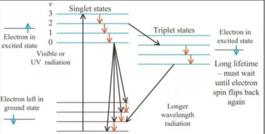
PhosphorescencePhosphorescence occurs when the material does not emit light immediately after being excited, due to the energy transition in quantum mechanics.
As we can see in the figure 1-2, we have a first stage in which the material is excited to higher energy states, then undergo an intersystem crossing into energy state of higher spin multiplicity, the singlet change his status and a part of the energy is used to do a spin-flip, from a singlet to a triplet S1→T1 (intersystem
17
crossing). Normally the transition T1→S0 is forbidden, which is why the lifetime of triplet states (phosphorescence) is longer than that of singlet states (fluorescence).
Figure 1 - 2: Phosphoresence main stages.
1.3.3 Electroluminescence
Electroluminescence is the light emitted by a solid through which an electric current is passing, in addition to its normal thermal emission. It implies the presence of electronic excited states with populations larger than their thermal equilibrium value.
Most of the electroluminescent solids are semiconductors. Light is produced by recombination of electrons and holes that have been injected at the cathode and anode respectively.
Electroluminescence was first observed in silicon carbide (SiC) by Captain Henry Joseph Round in 1907. Round reported that a yellow light was produced when a current was passed through a SiC detector. The second reported observation of electroluminescence did not occur until 1923, when O.V. Lossev of the Nijni-Novgorod Radio Laboratory in Russia again reported electroluminescence in SiC crystals.
Electroluminescence in organic semiconductors was firstly reported in 1963 and exploited as organic light emitting devices. On the other hand, electroluminescence in insulating polymers was firstly reported in 1967. So far, EL
18
in Polyethylene (PE), Polypropylene (PP), Polyethylene terephthalate (PET), Polyethylene Naphthalte (PEN), Polytherimide (PEI), Polyimide (PI), Polyethersylfone (PES), Polyvinyl Chloride (PVC), et. al., have been observed and studied.
In EL, electrical energy is transformed into light. To radiate in the visible portion of the spectrum, the luminescence centre must have an excited state of ≥ 2 eV higher than the ground state. The most important and interesting issues to reveal are: as how the radiative system is excited, and as which the light generation mechanism itself is.
a) Electroluminescence mechanism in dielectric materials
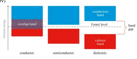
In electroluminescence we have electric field as excitation source, it follow different excitation processes. In the Figure 1-3 is shown the energy band diagram of conductor, semiconductor and insulator (dielectric).The most straightforward mechanism of EL excitation is direct field ionization of a centre. This effect involves electron tunnelling from the valence band to the conduction band (Zener effect) which occurs in semiconductors with a band gap of about 1-3 eV. It could not play any role in a large band gap insulator (beyond 5 eV).
Figure 1 - 3: band gap in conductor, semi-conductor and dielectric materials.
A second excitation process is the inelastic collision of a high energy electron, a so-called hot electron, with a centre (Destriau effect). The kinetic energy of the carriers is directly involved in the excitation process. A third mechanism is bipolar
19
charge carrier generation and subsequent electron-hole recombination which does not involve carrier kinetic energies, but does involve their potential energies. These last two processes have been studied quite extensively in connection with the dielectric breakdown strength of solids.
The excitation process in insulating polymers is localized in given molecular orbit or at luminescent centres, leading to the formation of excitons. An exciton is a bound state of an electron and a hole that are attracted to each other by the electrostatic Coulomb force, which is regarded as an elementary excitation that can transport energy.
b) Relaxation process and possible luminescent centres
Once the excited state has been formed, its de-excitation involves different pathways. Among the different possible mechanisms, one can distinguish two main classes: chemical, i.e. irreversible pathway and physical, i.e. reversible pathway. Both this classes of transitions can be radiative and non-radiative. In a physical process, the excited centre returns to its ground state without any chemical reaction. In a chemical reaction, the excited states can dissociate into molecular fragments which can be very reactive and lead to further chemical reactions. The balance between these two mechanisms is obviously very important for the relationship between electrical degradation and EL emission. If EL involves only physical processes, it would be a way to probe the excitation rate. If chemical processes are involved, EL can also be due to radiative de-excitation of degradation products and could provide a way to measure the dissociation rate. So in both cases, EL is considered as a potential ageing warning.
In relation to the luminescent centres, the pure carbon chain C-C or C-H single bonds in insulating polymers cannot perform as luminescent centres in the UV-visible domain, because the energy level transitions in these bonds are transitions at the extreme ultraviolet domain with high energy (8 eV or so).
Therefore, in a polyolefin polymer like polyethylene or polypropylene, there is normally no emission from the repeat unit due to aliphatic structure of the chains. So, if luminescence is detected, it is necessarily due to some types of possible chromophore groups in the carbon chain.
20
However, which chemical structure is actually excited and act as the chromophore under electrical field is still unknown issue according to previous works. It is still difficult to localize the definite luminescent centres by experimental work and simulations. Nevertheless, spectral analyses can help to investigate the source of the light emission. Works are carried out to uncover the nature of luminescent centres in these insulating polymers.
A further difficulty is the possible envolvement of electrode related emission –so called surface plasmons –SP- as explained below- when using gold or silver as electrodes for the material: the emission from insulating material would be superimposed to that from the electrodes. Figure 1-4 shows an example of such spectra obtained on XLPE with Ag electrodes [23] where emission at 750 nm has been ascribed to SP emission.
Figure 1 - 4: AC-EL spectra from Poly(ethylene naphthalate) films with Ag electrodes [23].
c) Electroluminescence and electrical ageing
The dielectric materials could be subjected not only to electrical stress but also to thermal, mechanical, chemical and environmental stresses. The mutual action of these stresses causes chemical changes to the polymer, eventually resulting in degradation and catastrophic failure of the system.
The mechanisms of ageing in insulating polymers submitted to electrical stress are not well known from a chemical standpoint, partly because of lack of techniques that are sensitive enough to detect the mild changes which are produced, and
300 400 500 600 700 800 0 50 100 150 200 (5) (4) (3) (2) (1) (1) 20 kV/mm (2) 50 kV/mm (3) 90 kV/mm (4) 130 kV/mm (5) 160 kV/mm N or m al iz ed E L Wavelength (nm)
21
partly because a low level of degradation is sufficient to initiate breakdown. Electric fields, through space charge effects, may produce excited or ionized states of the constitutive groups of the polymer, which can be involved in a subsequent chemical reaction. Some of these excited species have a non-zero probability for light emission during their relaxation. This light is called electroluminescence (EL). Therefore, the EL should in principle bring information on the nature of the recombining centres, which may have some relation with the initial centres of degradation. For the above described reasons the EL is an appropriate technique to detect the initiation of electrical breakdown in insulating polymers. Hence, EL is of double interest: on the one hand, it may provide information on the stress threshold for degradation and, on the other hand, it may help in identifying the nature of the defects where degradation originates.
The ageing sources can be several. They may have different origins: electrical, mechanical, ultraviolet (UV), chemical, thermal and water stresses. Each source may cause different ageing mechanism and thus to affect the electrical insulation in different ways. They could all have an influence on the formation of space charge (SC) within the polymer.
Furthermore, the EL is the only direct experimental evidence of the existence of potentially dangerous excitation energy in insulating polymer during ageing.
An important characteristic of EL, detected in many different polymers under AC and DC fields is that the light emission increases linearly with the applied field above a critical value.
The onset of EL changes from an insulating polymer to another due to their intrinsic electrical properties, for that reason we can say that onset of EL corresponds to the start of excitation mechanism which is universal among the insulating polymers. The EL onset voltage could represent a warning of electrical ageing.
With luminescence techniques, we can carry out light emission from each single process, such as recombination process and chemical reaction process, for analysing. This provides more information of EL, which proves EL is a multi-excitation involving physical and chemical processes under electric stress.
22
1.4 Surface Plasmons
We have briefly addressed above the possibility that EL from Ag or Au metallized samples be partly due to emission radiated during relaxation of surface plasmons. We describe here the nature of surface plasmons.
1.4.1 Introduction
A plasmon is a quantum of plasma oscillations. Just as light, viewed as optical oscillation, consists of photons, the plasma oscillation consists of plasmons. The plasmon can be considered as a quasiparticle since it arises from the quantization of plasma oscillations, just like phonons are quantization of mechanical vibrations. Thus, plasmons are collective (a discrete number) oscillations of the free electron gas density. For example, at optical frequencies, plasmons can couple with a photon to create another quasiparticle called a plasmon polariton [24].
Volume plasmons in a metal are longitudinal density fluctuations of the electron gas, plasma oscillations that propagate through the metal. They can be excited by a supply of energy, through either photon or electron irradiation. The quanta of these volume plasmons have energy ħ = ħ 4 / , (of the order of 10 eV), where is the conduction electron density, ħ is the reduced Planck constant, is the plasmon frequency, is the elementary charge and is the electron mass. They are produced by electrons which are shot into the metal.
An important extension of the plasmons physics has been accomplished by the concept of surface plasmons (SP). By extension a SP can propagate along a metallic-dielectric interface with a broad spectrum of eigen-frequencies from = 0 to SP p 1 d , depending on the wave vector k. The frequency of a SP in a metal is thus necessarily lower than that of volume plasmons. The electromagnetic field has a maximum at the metal-dielectric interface and decays exponentially in the direction perpendicular to the interface, as is characteristic for surface waves, cf. Figure 1-5.
23
Figure 1 - 5: interaction between a metallic and a dielectric medium.
1.4.2 Coupling
surface
plasmons
and
photons:
conditions for radiate relaxation
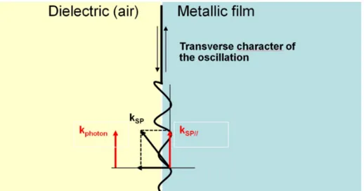
SPs at a perfectly smooth interface do not radiate light because their momentum is parallel to the surface and it is always greater than the momentum of photons of the same energy. The coupling conditions between the two particles are the energy conservation and the momentum conservation. If we can consider the same energy for SP and photon, the same cannot be said about the momentum.
This prevent the momentum conservation condition to be fulfilled which states that during the coupling, the components of the momentum of the two quanta parallel to the surface, ∥ must be conserved.
The surface roughness, as we can see in figure 1-6, provides smaller components of the SP wave vector parallel to the surface ∥, leading to the possibility of
radiative decay of SP in the visible domain.
The scale of roughness which is needed to couple SP with optical photons is from 1 to 100 nm, features that are naturally obtained with metallic layers deposited by conventional methods, sputtering of a metallic target or thermal evaporation of a metal.
The radiative de-excitation of SP has been observed in various metal-insulator-metal (MIM) structures biased under different voltages. In tunnelling junctions, a
24
thin insulating layer ( 10 nm) is used to control the tunnelling current which excites SP on the electrodes. The effect is similar to that obtained in a scanning tunnelling microscope.
Figure 1 - 6: Interaction between a metallic film and a dielectric medium in presence of a rough surface. Coupling condition for a surface plasmon and a photon.
1.4.3 Spectral distribution of the light emitted by SP
The other necessity is having a volume plasmons in the relevant energy range (visible or UV), as in the case for noble materials (Ag or Au). The maximum frequency of the optical emission follows the relation = ħ , being the electronic charge and the voltage applied between the electrodes of the MIM structure or between the electrode tip and the metallic surface in the tunnelling microscope [24].
Consequently, the spectral distribution of the light emitted by SPs depends on the properties of the metallic layers and the excitation conditions. The shape of the spectral output depends on several factors, such as: the energy distribution of the carriers that excite the SP modes, the surface roughness profile of the electrode, the energy-dependent internal damping of SP modes. It follows that there is variability in the emission spectrum due to SP from one sample to the other. On the other hand, the optical emission due to SP excited on different metallic layers,
25
especially in gold electrodes, exhibits an emission spectrum peaked in the red (620 to 850 nm) over a wide range of excitation conditions.
1.4.4 SP implication in electroluminescence spectra
The implication of SP in the red component of EL is consistent with several experimental observations. For example, in the Figure 1-7 we can see the emission spectra of an AC field EL for different MIM structures.
300 400 500 600 700 800 0 20 40 60 80 100 In te n si ty ( a .u .) Wavelength (nm) (1) (2) (3) (4) (5) (6)
Figure 1 - 7: Emission spectra due to SPs related emission in Metal-Insulator-Metal structure of different nature. Low field EL spectra of (1) Ag-Polyethylene Naphathalate-Ag, (2) Ag-PE-Ag and
(3) Au-PE-Au, (4) due to surface plasmon in a MIM structure. (5) SPs from BOPP, (6) SPs from XLPE.
The excitation of SP by charge injection/extraction needs a critical current density at the electrode surface. Imaging EL in the plane of the sample gives the relevant information to discuss this process in the case of highly resistive materials such as PE and PEN.
Under DC excitation, for example, the emission spectrum does not exhibit any particular emission in the red, i.e. the conditions for SP excitation are not fulfilled. To the contrary, imaging shows a strong localization of the emission at preferential spots in the sample plane when EL is excited under AC conditions, and the emission spectrum exhibits the red component. In the latter case, conditions are fulfilled for SP excitation.
26
Under AC stress, alternative injection and extraction of charge carriers at the electrode surface leads to high local current density around the sites which favour charge transfer, and thus SP excitation by charge injection/extraction can be fulfilled. Under DC, injection starts around the same sites, but due to the screening effect of the charge, the field is relaxed around these spots. EL is excited in the bulk material and SP excitation is not fulfilled at the electrodes [24].
There are many experimental facts inclining, as we said, for an emission process occurring at the contact of electrode/polymer under AC, due to charge injection-extraction at the interface. This also explain the fact that the red component is not detected under DC because the EL comes from the bulk of the sample, in that case, contrary to the AC where charge exchange is mainly occurring at the contact.
Another theme we will debate in this dissertation, with the support of some experimental measurements, is the fact that the red component is not observed with ITO electrodes under AC, this is another evidence that the source is located at the contact.
1.4.5 Silver nanoparticles (AgNPs) as the most
appropriate nanostructures to support surface plasmons
Noble metallic nanoparticles (NPs) are widely studied for different applications like for enhanced optical spectroscopies of molecules [25], nonlinear optics [26;27], photothermal therapy [28], photovoltaics [29;30], biocide effects [31;32] or more recently in plasmo-electronics [35;34], photocatalysis [35;36;37] and charge transport control [19] but mainly for their exceptional optical properties. In the past decade, a particular attention was paid on noble metallic NPs because they support localized surface plasmon resonance (LSPR). These collective oscillations of the conduction band electrons enable strong optical absorption and scattering in subwavelength structures, with spectral properties depending on the NP material, size, shape, electronic charge and surrounding medium. Among all noble metal NPs, AgNPs realize the best nanoscale antennae in the visible range of the spectrum (Figure 1 – 8). In this section, we will briefly describe the electronic and optical properties of noble metal NPs.
27
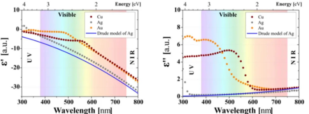
Scaling down to nanometer size, the optical response of metals is affected by three main features: size, shape and surrounding medium of the metal. The complex dielectric function of metal nanoparticles develops size dependency in the nanometer range. The size dependency of dielectric function stems from both interband transitions and damping contributions with the later contribution usually exceeding. The damping involves changes in the electronic mean free path due to the scattering of conduction electrons against the nanoparticle surface.
Figure 1 -8: Experimentally obtained real part ’() and imaginary part ’() of the dielectric function of Cu, Ag and Au (color points) for bulk materials. The blue line represents the calculated
dielectric function according to Drude model. Adapted from A. Pugliara [38].
In the same way that we have described the surface plasmons along the metal/dielectric interface, we can define the localized surface plasmon as the quantum of collective oscillations in a NP. The corresponding resonance or LSPR takes place for a frequency:
, 2 p LSPR IB d
where p() is the plasma frequency, IB() is the part of the complex dielectric
function due to the interband transitions in bulk metals and d() is the dielectric
function of the surrounding dielectric medium. This frequency depends on the NP material and shape (here the factor 2 is the shape factor for a sphere) but also on the environment (d) of the NP. Thanks to their small size, the NPs allow to
concentrate the electromagnetic field at a scale drastically smaller than the corresponding wavelength. This is particularly suitable to the use of the exaltation
28
effects of the light diffusion by objects localized in their near field as the well-known SERS (Surface Enhanced Raman Spectroscopy) effect [39].
The resonance frequency LSPR of a spherical NP, and therefore the associated
photon energy, depends on the nature of NP material but also on that of its embedding matrix. We can hence calculate the resonance energy of the composite system if we know the dielectric functions of the both materials. The calculation of the extinction efficiency gives information on the resonance profile (frequency location, width and intensity) and allows the best choice of the couple (NP material/matrix). In Figure 1 - 9, the extinction coefficient for NPs made of 3 noble metals (Ag, Au and Cu) in two different matrices (SiO2 and Si3N4) is plotted
[39]. The relative amplitude of each curve clearly shows an important resonance for Ag and Au that can be used for plasmonic applications in these two types of matrices. Nevertheless, the Ag resonance is clearly higher than the one of Au and this material is better for maximum field exaltation. Indeed, the resonance quality factor, defined as Q = λLSPR/λ where λ is the FWHM, is higher for AgNPs than
for AuNPs (metal effect) because of the supplementary damping by interband transitions in Au. By changing the embedding medium, from SiO2 (SiO2 = 3.9) to
Si3N4 (Si3N4 = 7.5) for example, a strong enhancement of the LSPR and tuning in
the middle of the visible can be obtained. The LSPR of AgNPs shifts from the near UV range (400 nm) to the visible range (475 nm). Owing to the fact that the higher the refractive index, the better the electromagnetic energy confinement is, the quality factor is doubled when changing the surrounding medium from SiO2 to
Si3N4 for example. Nevertheless, most of the studies in the literature describing
AgNPs embedded in dielectrics for plasmonic applications involve silica matrices. The optical response of AgNPs is used in this work for non-destructive characterization of polymeric materials.
29
Figure 1 - 9: Extinction efficiency of noble metal NPs embedded in a SiO2 (a) and Si3N4 (b) matrix [39].
1.5 Purpose of the thesis
The idea of this dissertation is to start from the results obtained by B. Qiao in his thesis and, during the first part of this work, to repeat some experimental measurements aiming at a firm confirmation of the observed features.
For this reason, our samples will have MIM (Metal-insulator-metal) configuration. The metal deposited on the polymers, BOPP (Bi-axially Oriented Polypropylene), will be gold (Au) or ITO (Indium Tin Oxide).
In the figure 1-10 we can see the experimental situation with gold as semi-transparent metal sputtered on the surface of the insulator.
Figure 1 – 10: structure of an Au-BOPP-Au sample.
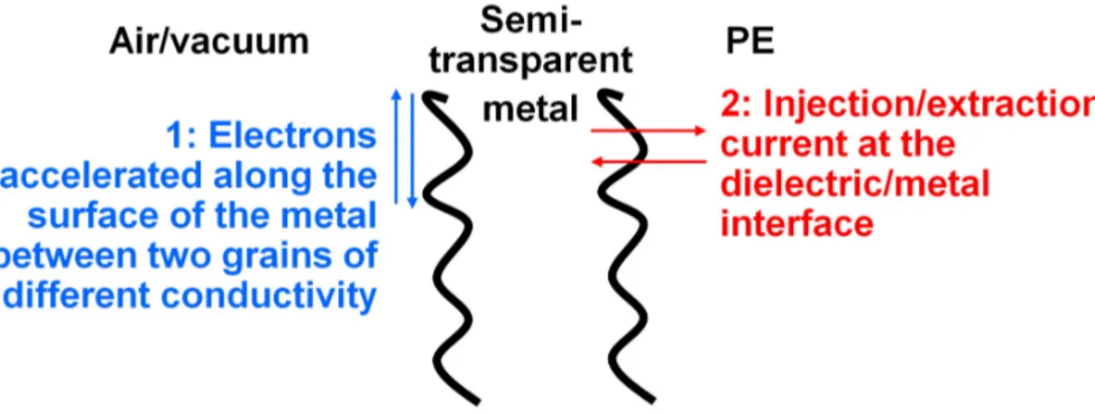
In this case, during EL measurement, surface plasmons are generated by electronic current due to polarity change with two possible origins (cf. Fig 1-11):
1. Injection or extraction of current at the metal(electrode)/dielectric interface; BOPP 17.8 µm
Gold
30
2. Surface current between metallic particles in case the electrode not constitute a perfectly continuous layer. We remind that thin metallic electrodes are used (come tens of nm thickness) to get reasonable light transmission through it.
Figure 1 – 11: Interaction between vacuum, metal and BOPP. Two SP can potentially develop: at dielectric-Au interface and at Au-vacuum interface.
In Figure 1-12 we can see a schematic situation during the positive half cycle applied to the electrode all along an EL measurement:
Figure 1 – 12: Interaction between vacuum, metal (electrode) and BOPP.
31
Electrons with a low kinetic energy (2) or trapped near the interface will be collected by the metal and relaxed at the dielectric-metal interface (5). Electrons with a higher kinetic energy (1) can be injected into the metal and
relaxed (4) on their way to the metal-vacuum interface. If they have sufficient kinetic energy, they can excite SP at the interface (6). This will depend on: the kinetic energy of the electron, the thickness of the metallic layer, the scattering length of hot electrons into the metal. Thickness of 100 nm to 500 nm is pertinent for kinetic energies of 10 eV.
In the second part of my work intends to check the SP hypothesis by changing the structure of the sample. The idea is to keep the same arrangement, same thickness of the different layers, and to deposit a mono layer of AgNPs embedded in an organosilicon (SiOC:H) matrix on the top of BOPP substrate. Although the SiOC:H matrix is known as low-k material, with dielectric constant between 2.0 and 3.0 depending on the elaboration process, it was selected to better adapt to the polymer (plastic) substrate. Then cover both sides with an ITO layer to form the final structure under study, cf. Fig. 1-13.
Figure 1 - 13: Structure of the multi-layer sample (ITO-BOPP-AgNPs- SiOxCy:H-ITO).
The investigated process will be the impact of the confinement of the metal into nanoparticles on the SPs effects, along with supporting information on the role of deep traps from AgNPs previously reported under DC stress.
SiOxCy:H
ITO BOPP 17.8 µm
AgNPs
32
1.6 Plasma deposition techniques for synthesis of
AgNPs in silica-like matrix
One of the purposes of this thesis will be to investigate EL from metallic nanoparticles containing nanocomposite ultra-thin films. Therefore we purpose a brief state of the art on deposition processes.
1.6.1 Introduction
Plasma based deposition of thin films is largely applied in industrial applications [40]. Starting in the microelectronic domain in the early 80’s of the last century, the plasma technologies for deposition have now place in different areas of our every day’s life, like for example in optics for coating layers, for surface treatment in the food industry, for biomedical applications, in photovoltaics’, etc. Depending on the type of the used gas discharge, the main plasma characteristics (electron density and electron energy), the reactive gases injected as precursors and the gas pressure, one can obtain a quite large variety of composition of deposited thin layers, including elaboration of nanocomposite materials. Principally, the Physical Vapor Deposition (PVD) and the Plasma Enhanced Chemical Vapor Deposition (PECVD) are used in the surface modification of a wide range of substrates. In particular, PVD involves the evaporation or sputtering of a solid material while in PECVD the plasmas are used to activate the chemical precursors and consists of applying different types of gas discharges. The advantage of these deposition methods concerns the huge versatility and the excellent control of thin film growth at micrometric and nanometric scale [18;19;31;32;40;41;42;43;44;45;46] Industrial plasma reactors are usually supplied with alternative current (AC) and depending on the used gas discharge they work in the whole range of pressure variation, from low pressure up to atmospheric pressure. Without loss of generality the discussion here is limited to an axially-asymmetric radio-frequency (RF) capacitively-coupled discharge sustained at 13.56 MHz at low gas pressure. This plasma deposition process has been chosen to elaborate a layer of AgNPs embedded in the organosilicon layer for our studies.
33
1.6.2 Plasma Enhanced Chemical Vapor Deposition
(PECVD)
Versatility of plasma based deposition processes is widely used for technological purposes. Plasma enhanced chemical vapor deposition (PECVD) processes have now place in different areas of our every day’s life, like for example in optics for coating films, for surface treatment in the food industry, for biomedical applications, in photovoltaics’ domain, etc. [40]. Depending on the type of operated gas discharge, the main plasma parameters (electron density and electron energy), the reactive gases used as precursors and gas pressure, one can obtain a large variety of composition of the deposits, including nanocomposites [44]. The possibility to design complex nanocomposite thin layers is determined by the complexity of the medium itself. The properties of non-equilibrium plasmas as media actually represent key elements in the synthesis of nanocomposite thin films offering a high degree of freedom in their elaboration.
RF capacitive coupled discharges are by far the most widely applied ones for thin film depositions, entirely compatible with the microelectronic technology. Moreover, in hybrid plasma deposition methods, by combining PECVD and sputtering, nanoparticles can also be composed of the sputtered material [41;43]. Such systems thus represent interesting building blocks for deposition of multifunctional, nanocomposite thin films. Nanocomposite materials consisting of AgNPs embedded in dielectric matrices present a huge interest as plasmonic substrates. The main advantage of these assemblies is the possibility to manipulate, localize and enhance the electromagnetic field at the structure surface. To take benefit of the hybrid plasma deposition when the sputtered target is a silver material at LAPLACE Laboratory they have developed a strategy to elaborate large area plasmonic substrates [32; 46; 47].
In the electrical engineering domain, the phenomenon of charge injection in dielectric layers under electrical stress is at the origin of space charge formation. For many industrial
purposes, like for high voltage DC (HVDC) applications (e.g. HVDC cables with polymeric insulation), the space charge must be avoided because it gives a contribution to the electric field distribution by modifying the latter compared to the
34
designed one and represents a risk for breakdown, especially under voltage reversal [48; 49; 50]. In order to resolve this problem, in views of the intrinsic difficulty in controlling the contact between polymeric material and the electrode (metal or semi-conductor), the solution can be to use a thin layer of nanocomposite material with adequate properties in between the electrode and the polymer to control the injection process to the polymeric material defects or traps. This nanocomposite layer contains a single layer of AgNPs embedded in an organosilicon matrix. Due to the ability of AgNPs to store electrical charges they are supposed to play the role of deep trapping centres thereby stabilizing the injection, implying thus a field reduction at the electrode when the nanograins are charged. The control of charge injection phenomenon certainly improves the performance and increases the reliability of dielectric materials [18; 19; 20; 51]. The addition of AgNPs layer on our BOPP substrate with the application of a plasma deposition process, we want to tailor the surface of the dielectric materials by a multifunctional layer for elaboration of large-plasmonic embedded substrates. After that the mission is to investigate the optical properties of the new multilayer sample to understand the effect of AgNPs.
35
Chapter 2 Experimental Materials and
Techniques
2.1 Materials (Polypropylene)
Polypropylene (PP) is a polyolefin, composed of monomers - 3 6-, with the
chemical formula ( 3 6) 2, widely used in industries since invented in the early
1950s. The commercial production of PP began in 1957 in USA and 1958 in Europe [56]. It is a thermoplastic polymer widely used in a variety of application including packaging, textiles, and electrical equipment components, such as capacitors and electrical accessories. It is liable to chain degradation from exposure to heat, UV radiation, and under electric field.
Samples are extruded between two rolls and manufactured in thin films for capacitor applications with high breakdown strength.
When Polypropylene film is extruded and stretched in both the machine roll direction and across machine roll direction, it is called Bi-axially Oriented Polypropylene (BOPP). All the measurements are carried out in this dissertation on BOPP films of 17.8 µm thickness supplied by KOPAFILM, Germany. The films were provided with different roughness for the faces, to favour oil impregnation. The only known additives contained in the BOPP films under study are penta-erythritoltetrakis (3,5-di-tert-butyl-4 hydroxyhydrocinnamate) and calcium stearate. The former is known as Irganox 1010, which is a sterically hindered phenol used as an antioxidant to abstract unstable radicals. Calcium stearate is a lubricant and an acid scavenger used to neutralize any hydrochloric acid generated from reactions between the hindered phenol and residual chloride-containing catalyst [53].
36
2.2 Experimental setups
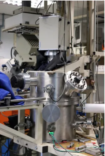
In the dissertation, Leica EM ACE600 system is utilized to deposit gold (Au) and Indium Tin Oxide (ITO) electrodes. Figure 2-1, represents a picture of the Leica EM ACE600 system. It is a versatile high vacuum film deposition system designed to produce very thin, fine-grained and conductive metal and carbon coatings for high resolution analysis, as required, for example, for FE-SEM and TEM applications. This high vacuum coater can be configured for the following methods: Sputtering, Carbon thread evaporation, Carbon rod evaporation, E-beam Evaporation and Glow discharge.
Figure 2 - 1: Leica EM ACE600 system.
The luminescence analysis system used in this work is a lab-made test bench to measure the photoluminescence (including fluorescence and phosphorescence), electroluminescence, and cathodoluminescence from solid materials.
For the AgNPs deposition a special plasma reactor developed in LAPLACE is used: it exploits the plasma of an axially-asymmetric capacitively-coupled RF (13.56 MHz) discharge sustained at low gas pressure.
37
2.2.1 Sample preparation
a) Gold metallization setup
To perform the EL measurements, electrodes must be deposited on the studied samples to apply a controlled electric field. Besides, the deposited electrodes must be partially transparent in the UV-VIS domain in order to collect light.
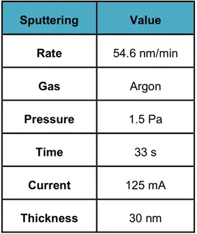
The films are deposited uniformly at a deposit rate of 54.6 nm/min. The insulating polymer films are thus provided with gold electrodes having diameter of 50 mm and a thickness of 30 nm. The parameters of the sputtering are listed in Table 2-1. The sputtering pressure is about 1.5 Pa in Argon plasma. The current is 125 mA.
Sputtering Value Rate 54.6 nm/min Gas Argon Pressure 1.5 Pa Time 33 s Current 125 mA Thickness 30 nm
Table 2 - 1: Parameters of the sputtering process of gold.
b) ITO sputtering setup
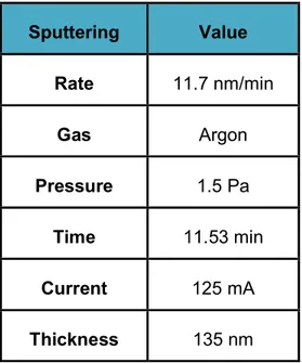
The Leica EM ACE600 system can also be used to deposit Indium Tin Oxide (ITO) on the surface of a polymer films. Improvement of this industrial system has been made by the technical staff of LAPLACE, especially to improve the vacuum level and purity of the Argon into the deposition chamber. The deposition rate, in this case, is different: 11.7 nm/min. Also the deposition time change with this process:
38
11.53 min. The transparency of ITO is approximately 90 %, while the surface electrical resistance is found 16x10-3 Ω/cm2.
Sputtering Value Rate 11.7 nm/min Gas Argon Pressure 1.5 Pa Time 11.53 min Current 125 mA Thickness 135 nm
Table 2 - 2: parameters of the sputtering process of ITO.
c) Treatment of electrode edges
At the end of the sputtering process (Gold or ITO), before introducing the sample inside the multi-purpose chamber, it is necessary to apply a layer of silicone elastomer along the border of the sputtered zone. The ribbon avoids discharges and flashovers due to field strengthening at electrodes edges. To do so, a protective film (PP) is pressed on the silicone and kept in place for one or two days up to complete the vulcanisation in air. During my stay at LAPLACE laboratory I’ve developed a new process to apply the silicone elastomer and the protective film to reduce the process time and to improve removing the protective film without damaging the sample.
The new process involves making a hole (diameter of 44 mm) with a hollow punch in the protective PP film and applying the holed film on the silicone. It is possible in this way to run the EL measurement without removing the protective film. In the Figure 2-2 we can see a picture of the complete sample with Au electrode.
39
Figure 2 - 2: picture of a complete Au-BOPP-Au sample.
2.2.2 Luminescence setup
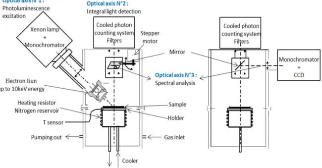
All the luminescence experiments were carried out in a multi-purpose chamber as shown in Figure 2-3. It mainly contains five systems:
1. Excitation source system (electric field, through high voltage feedthrough, electron beam, for cathodoluminescence and UV-vis photons for photoluminescence);
2. Optical detecting system (PM system and CCD camera system); 3. Optical path controlling system;
4. Temperature controlling system; 5. Pumping system.
The excitation system and the optical detecting system are the core parts for luminescence measurements, while the other systems are auxiliary components. The detecting system is composed by two parts according to the optical axis: optical axis No.1 is photoluminescence excitation source; optical axis No.2 a Peltier system cooled photomultiplier (PM) working in photon counting mode for integral light detection; optical axis No.3 a grating dispersive system (4.5 nm in resolution) coupled to a liquid nitrogen cooled charge coupled device (CCD) camera for spectral analyses which covers the wavelength range from 230 nm to 840 nm.
40
The core of this multi-purpose system is a light proof dark chamber connected to a turbo-molecular pump system to achieve high vacuum at 10-4 Pa in order to avoid gaseous discharge during measurements. Samples can be placed on the holder which contact to a heating resistor, a nitrogen reservoir, and a temperature sensor, to control the temperature from liquid nitrogen temperature up to 150°C. The multi-purpose chamber is designed to accommodate different kinds of luminescence excitation. Picture of the system is given in Figure 2-4.
Figure 2 – 3: schematic of the multi-purpose chamber.
a) Excitation source
In the system that we are introducing here, we can use three different types of excitation sources: a) electric field excitation, b) optical excitation and c) electron beam excitation.
The optical excitation is usually used during photoluminescence (PL) measurement, the sample mounted into the chamber at ambient atmosphere were excited by a xenon source coupled to an irradiation monochromator.
The electron beam excitation is used for cathodoluminescence (CL) measurement, a home-designed electron beam gun mounted into the chamber,
41
providing electrons of up 10 keV in energy. The filament is at negative high voltage and the anode at the ground.
However, in this dissertation we will mainly show results obtained previously by CL on PP films [58] and will compare these spectra to the newly acquired ones. New results are mostly with electric field excitation.
Figure 2 – 4: picture of the luminescence experimental setup.
During electroluminescence (EL) measurement, the configuration of Figure 2-5 was installed in the dark chamber and put under high vacuum. All the measurements are carried out at room temperature. Light detection can be carried out by two systems PM and CCD. The two electrodes HV tin electrode (inner diameter 30 mm) and ground flat electrode (diameter 40 mm) are connected to the high voltage and ground respectively. The ring electrode allows the light emission analyses from the centre of the sample.
![Figure 1 - 9: Extinction efficiency of noble metal NPs embedded in a SiO 2 (a) and Si 3 N 4 (b) matrix [39]](https://thumb-eu.123doks.com/thumbv2/123dokorg/7424737.99170/31.918.241.756.107.302/figure-extinction-efficiency-noble-metal-nps-embedded-matrix.webp)