University of Pisa
Engineering Ph.D. School "Leonardo da Vinci"
Ph.D. Program in Information Engineering Micro and nanoelectronic technologies, devices and systems
High-Voltage Integrated Circuits design and
validation for automotive applications
Thesis
Giuseppe Pasetti
Year 2009-2011
Tutors: Prof. Luca Fanucci . . . .
Prof. Roberto Saletti . . . .
Ing. Riccardo Serventi . . . .
Abstract
Electronic Integrated Circuits (ICs) are an important pillar of the automotive market, especially since legal and safety requirements have been introduced to manage vehicles emissions and behaviors. Furthermore, the harsh environment and the tight safety requirements, summed with the market that is pushing to reduce the development lead time and to increase the system complexity, require to develop dedicated ICs for the automotive applications.
This thesis presents some peculiar high-power and high-voltage ICs for au-tomotive applications that have been studied, designed and developed taking into account all the requirements that automotive grade ICs have to respect, with emphasis on performance, quality and safety aspects. Particularly the thesis reports the design and validation of power management blocks and out-put drivers for inductive loads, showing how to fulfill in an effective way the performance, quality and safety targets according to the guidelines and the constraints of the latest automotive standards, like ISO26262 and AEC-Q100. All the designed ICs has been simulated and manufactured, including layout drawings, in a 0.35µm HV-CMOS technology from AMS. The effectiveness and robustness of the proposed circuits has been validated on silicon and corre-sponded measurement results has been reported.
Contents
Abstract i
1 Introduction 1
1.1 Design for Performances . . . 4
1.2 Design for Quality . . . 4
1.3 Design for Safety . . . 6
1.4 Scope and organization of the thesis . . . 8
2 HV IC design for automotive switching regulators 11 2.1 Switching voltage regulators . . . 11
2.1.1 Linear voltage regulators . . . 13
2.1.2 Switching voltage regulators . . . 14
2.1.3 Control techniques . . . 15
2.2 Designing a switching voltage regulator . . . 17
2.2.1 Block diagram . . . 18
2.2.2 Layout . . . 20
2.3 Validation: simulations and measurements . . . 21
3 Drivers for inductive loads 25 3.1 Solenoid Valve Driver . . . 27
3.1.1 Design . . . 28
3.1.2 Layout . . . 32
3.1.3 Quality and safety aspects . . . 33
3.1.4 Validation . . . 34
3.2 Rotor Coil Driver . . . 41
3.2.2 Layout . . . 50
3.2.3 Quality and safety aspects . . . 51
3.2.4 Validation . . . 52
4 LED Driver IC design for automotive lighting 57 4.1 Flexible LED driver IC . . . 59
4.2 Validation . . . 62
5 Voltage regulators for automotive alternators 65 5.1 New alternator development . . . 70
5.2 IC design . . . 72
5.3 Quality and safety aspects . . . 76
5.4 Validation: simulations and measurement results . . . 77
Conclusions and Outlook 81
Publications 83
List of Figures
2.1 Electronic Voltage Regulator block diagram . . . 12
2.2 Linear Voltage Regulator block diagram . . . 13
2.3 Switching Voltage Regulator block diagram . . . 15
2.4 Voltage control scheme. . . 16
2.5 Current control scheme . . . 17
2.6 Regulator block diagram . . . 19
2.7 Regulator layout . . . 20
2.8 Normal mode waveform . . . 21
2.9 VOU T vs VIN with 100mA output current . . . 22
2.10 VOU T vs VIN with 500mA output current . . . 22
2.11 Load Regulation with 5V supply voltage . . . 23
2.12 Load Regulation with 12V supply voltage . . . 23
3.1 Principles of typical solutions to handle inductive freewheeling . . . 25
3.2 Inductive driver block diagram . . . 28
3.3 Gate-driver and Zener-like circuits . . . 29
3.4 Diagnostic circuit . . . 30
3.5 Layout of 8 different inductive drivers . . . 32
3.6 Simulated turn-on transient . . . 34
3.7 Simulated turn-off transient . . . 35
3.8 UV flag Montecarlo simulation . . . 36
3.9 UC flag Montecarlo simulation . . . 36
3.10 OC flag Montecarlo simulation . . . 37
3.11 Measured turn-on transient . . . 38
3.12 Measured turn-off transient . . . 38
3.14 Measured UV flag . . . 39
3.15 Measured UC flag . . . 40
3.16 Connection of alternator output, battery and rotor coil with its driver . . 41
3.17 Alternator coil driver schematic . . . 43
3.18 PMOS vs. NMOS comparison during reverse battery condition . . . 45
3.19 Gate-Driver block diagram . . . 46
3.20 Gate-Driver transients . . . 48
3.21 ADC and monitors block diagram . . . 50
3.22 Alternator Voltage Regulator IC with the designed rotor coil driver . . . 51
3.23 Voltage and current in the rotor coil . . . 53
3.24 Slow current slope . . . 54
3.25 Fast current slope . . . 54
3.26 RDSonof the HV-PMOS vs. Temperature . . . 55
3.27 VSGof the HV-PMOS and Vdiode vs. Temperature . . . 55
4.1 Bulb (a) and LED (b) behavior with 10cm long connection cable . . . 58
4.2 Bulb (a) and LED (b) behavior with 3m long connection cable . . . 59
4.3 Highlight of wiring parasitic . . . 59
4.4 Architecture of the LED driver . . . 60
4.5 Layout of the LED driver . . . 61
4.6 Layout of the automotive IC with the LED driver . . . 61
4.7 Output voltage and current during the turn-on transient. . . 62
4.8 Output voltage and current during the turn-on transient. . . 63
4.9 Output voltage and current during the turn-on transient. . . 63
5.1 Exploded view of an alternator . . . 65
5.2 Regulated Alternator blocks and electrical connections . . . 66
5.3 Mechatronic top and bottom view . . . 67
5.4 Regulation loop principle . . . 68
5.5 Rotor excitation driver . . . 68
5.6 Assembled brush holder with the IC (left) and mezzanine board with the FPGA (right) . . . 71
5.7 Electronic system block definition . . . 71
List of Figures
5.9 Power up strategies . . . 75 5.10 IC microphotograph . . . 78 5.11 Measuring setup . . . 80
List of Tables
1.1 Consumer vs Automotive semiconductor requirements . . . 1
2.1 Regulator requirements . . . 18
3.1 Advantages/Disadvantages of typical solutions in Fig. 3.1 . . . 26 3.2 Operating and environmental ratings . . . 33 3.3 HV-PMOS and HV-NMOS operating and absolute ratings . . . 44 3.4 Rotor Coil Driver area occupation . . . 52 3.5 HV-PMOS and HV-NMOS operating and absolute ratings . . . 52
4.1 Wiring parasitic measurements . . . 62
1 Introduction
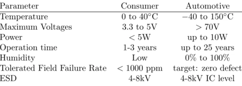
Since the last fifty years, the importance of electronics in automotive envi-ronment is constantly increasing, driven by the continuous requests to develop new safety and infotainment devices. This has led to a constant increase of the number of electronic devices and control units (ECUs) in the modern cars and today several hundreds of different ECUs can be found in a car, each one specialized to do a different task[1, 2, 3]. This has led to the need to develop au-tomotive specific integrated circuits (ICs), that have to operate in that harsh environment[4]. Indeed, compared with standard consumer ICs, automotive grade integrated circuits have very different environment requirements. The first simple mind environment difference is the ambient temperature[5]. Just think that cell phones have to work at maximum 60◦C, when they are operating in the Sahara desert, while all the engine related electronics have to work nor-mally with a temperature above 100◦C. The operating temperature and many other environment differences can cause standard consumer ICs to fail when trying to operate in the automotive field. Table1.1 shows the main differences between those two environments.
Table 1.1: Consumer vs Automotive semiconductor requirements
Parameter Consumer Automotive
Temperature 0 to 40◦C −40 to 150◦C
Maximum Voltages 3.3 to 5V > 70V
Power < 5W up to 10W
Operation time 1-3 years up to 25 years
Humidity Low 0% to 100%
Tolerated Field Failure Rate < 1000 ppm target: zero defect
ESD 4-8kV 4-8kV IC level
ve-hicle, like braking and steering systems, it is very important to guarantee the highest quality level and a "zero defect" rate during all the lifetime of those safety related systems.
On the other hand, the market is constantly pushing to implement new features increasing the complexity of the electronics in the vehicle. This has led to an increased number of electronic systems and stringent requirements for those systems.
For these reasons, the designer of automotive ICs has to take care of a huge number of different requirements, making its work very difficult. In fact, dur-ing the development phase of automotive ICs, the designers not only have to guarantee the functionality over the operative range of supply voltages and temperature, but have to take care of the absolute voltage and temperature ratings and consider the very stringent requirements about the IC and sys-tem level Electrostatic Discharge (ESD) protection performances and about the Electromagnetic Immunity (EMI) and Compatibility (EMC) of the IC and of the whole system.
Indeed, especially in the high voltage periphery part of automotive ICs, the absolute maximum rating can be very different from the operative. Spikes and surges events, which can appear in automotive environment, can seriously damage the Integrated Circuit if they are not correctly managed and filtered. Furthermore, automotive ICs have to avoid damages and manage correctly the permanent reverse battery condition, condition in which the supply voltage can stay below ground without time limitation, and the loss of ground event, when the ground connection is lost. In this case the ICs must detect it and signal it to the driver.
Moreover, as many different devices are close in the car, it is very important that every device don’t disturb and don’t be disturbed by the others. Indeed in the automotive environment, the devices are close together and shares the same supply and this can led the arise of issues when they operates concurrently. To avoid or limit these kinds of issues, the designer has to take care of the stringent requirements of EMI and EMC. Those aspects are very difficult to predict and simulate, as they mainly deal from parasitic components at IC and
PCB level and must be solved as high-frequency wave transmission simulator instead of circuit simulator.
Furthermore the designer has to check the operative region of every device to guarantee the target lifetime of the IC, recognizing possible weak devices and doing all the necessary modifications in order to increase the whole IC lifetime. Last but not least, like every battery powered system, the designer has to implement power saving techniques. Those techniques are necessary to reduce the total power consumption, increasing the discharge time of the battery when the engine is turned off and reducing the fuel consumption and CO2 emissions when the engine is running.
As said before, since the importance of electronics is constantly increasing in modern car, the main car makers and semiconductor suppliers have established the international Automotive Electronics Council (AEC) with the task of es-tablishing common part-qualification and quality-system standards. The AEC has defined the international AEC-Q100 standard, covering the quality require-ments for automotive integrated circuits.
Actually, every electronic system that is sold for automotive application needs to fulfill all the requirements defined in the AEC-Q100 standard, and then those requirements must be well considered in the development phase of automotive ICs.
At the end, during the development of automotive integrated circuits, there are many different forces that drive the design phase, that can be divided into three main sectors: the performances, the quality and the safety.
The rule of the designer is to balance those forces, finding the best solution for the target application and with the given requirements.
Indeed, there is not only one solution for every problem, but it can change depending on the system requirements. The good designer must be able to find the best approach for a given problem, modifying the system architecture and defining the needed performances for the single blocks that compose it.
1.1 Design for Performances
Designing for performances means to increase the overall performances of the IC. It can be done in several ways, like reducing the power consumption or implementing new functions.
Indeed in the automotive environment, the market, which is constantly pushing for innovative and cost-effective electronic systems, demands always more com-plex Integrated Circuits while at the same time requires to reduce the power consumption.
One important performance parameter is the power consumption. In fact, the car makers, to reduce the fuel consumption, need to reduce the total power consumption of the electronics in the car and one of the most important pa-rameter for them to choose an electronic system is the power dissipation.
Another important parameter is the system cost. One way to reduce it is to integrate on the same die different functions, reducing the number of elec-tronic ICs. This requires large design effort, because, when many systems are integrated on the same die, the interferences and the noise between them can reduce the overall system performances.
1.2 Design for Quality
Designing for the quality means to take all the necessary actions to ensure that the electronic part is working correctly and doing the one for which it was designed.
Those countermeasures permit to identify and discard the faulty devices, that are not working correctly at test, and the possible weak devices, that are func-tional at test but can reveal a latent fault during the device lifetime.
In order to reach the "zero defect" target, a combination of design, test and qualification must be mixed together, identifying all the possibles weaknesses
1.2 Design for Quality
from the early stage of the system design and implementing all the needed countermeasures to solve that. For this, many standardized design methodolo-gies have been implemented and they have been widely analyzed in literature[6, 7, 8, 9]:
• Design for Test (DFT)
• Design for Manufacturability (DFM) • Statistical Analysis
• High Temperature Operating Life (HTOL) • Burn-in / High Voltage Stressing
Design for Test
Testing ICs permits to locate and screen failing devices and having a complete coverage at test is necessary to reach the "zero defect" rate. The DFT is in charge to increase the observability and controllability coverage at test, adding special structures like the SCAN chain or testing analog multiplexer to have the possibility to read-out the voltage on internal nodes.
Design for Manufacturability
The DFM is based on the data of previous products from silicon foundry and permits to increase the production yield, implementing basic countermeasures on possible production related failures. For instance, they can cover metal sizing and spacing to limits the short and open failures related to the metal.
Statistical Analisys
The applying of statistical analysis during the test of the devices permits to recognize weak devices that have all parameters inside the specifications. For instance, PAT (Part Average Testing) method calculates the tester limits based on the statical distribution of the previous devices. In this way is possible to screen the devices that have some parameters far away from the other devices.
This can lead to a shorter lifetime, so screening those devices permits to increase the lifetime of device.
High Temperature Operating Life
The HTOL test is a reliability test and permits to estimate the lifetime of the device. That test requires the application of high temperature and voltage stress on the semiconductor devices over long periods for a small sample size, accelerating the aging of the devices and highlighting lifetime issues. This permits to evaluate the lifetime and failure rate of the larger population[10]. In fact, that test is very important to calculate the FIT (Failure In Time) and MTTF (Mean Time To Failure), which can estimate the lifetime of the semiconductor devices.
Burn-in / High Voltage Stressing
Those techniques permits to identify the latent defects, accelerating their manifestation, while operating at high temperature, during Burn-in, or at high voltage, in case of High Voltage Stressing.
1.3 Design for Safety
Designing for the safety means to take all the necessary actions that prevent harms and injuries to the users of the electronic system, when a fault condition occurs.
In this case, it is investigated the effect of a single or multiple faults on the system behavior and are minimized all the possible causes of injuries for the users.
Recently, a new automotive standard for functional safety, mainly focused on electrical/electronic systems mounted on series of passenger cars, has been de-veloped: the ISO26262 Road vehicles − Functional safety standard[11].
1.3 Design for Safety
but has been adapted for the automotive Electric and Electronic industry. Like the IEC61508[13], the ISO26262 rely on the following assessments on the risk:
• Zero risk can never be reached
• Safety aspects must be considered from the beginning • Non-tolerable risks must be reduced
Furthermore, compared with the IEC61508, the ISO26262 introduces the idea of controllability, which can be synthesized in the ability to avoid haz-ardous events by the action of the driver[14, 15].
In fact, the ISO26262 provides an automotive specific lifecycle and defines the necessary activities to do for each stage of the lifecycle, requiring to keep record of all the safety-related activities during the entire lifetime of automotive elec-tronic systems, from the early design to the out-of-production phases.
The ISO26262 standard defines an automotive-specific risk-based approach for determining risk classes (Automotive Safety Integrity Levels, ASILs) and di-vides the ASILs into four different levels: from the ASIL-A level, which cor-responds to fails that can cause no safety issues and has the lowest safety requirements, to ASIL-D, related to fails that can hazard the driver in case of failure and requiring the highest safety requirements, passing through ASIL-B and ASIL-C with intermediate safety requirements.
Each ASIL level specifies the necessary safety requirements, has its own process and defines the different steps for item development to achieve an acceptable residual risk, the residual probability of fault after that all ISO26262 actions has been taken.
The ASIL level depends on the combination of assessments[16] of:
• Severity • Exposure • Controllability
The Severity indicates the grade of possible injuries that the fault can gener-ate and is divided into four grades: from S0, which relies on non safety-relgener-ated failures, to S3, which coincides on faults that can generate life-threatening or fatal injuries.
The Exposure indicates the probability that the fault can occur. In the ISO standard, five different grades are defined: from E0, which means situations that occur less then once in the vehicle lifetime, to E4, which means situations that occurs during almost every drive on average.
The Controllability indicates the needed driver skills to avoid harm when the fault occurs. It is divided in four grades: from C0 to C3, while C0 means that all driver or other traffic participants can avoid a specific harm and C3 means that less than 90% or more of all driver or other traffic participants are usually able to avoid a specific harm.
Driven by the car makers requirements, in short time, this ISO standard is becoming the new reference for all the new developed electronic systems.
The ISO26262 requirements, that are related to the whole electronic system, can be easily reported to the requirements for the ICs that builds the system. In this case, the standard FMEDA approach can be successful[17, 18, 19].
1.4 Scope and organization of the thesis
The scope of this thesis work is to present the design and validation phases of innovative high voltage CMOS integrated circuits for automotive applications. During this thesis, all the aspects of the automotive design flow will be faced, focusing on the main difficulties that the IC designers will have to face to reach a working device and highlighting the chosen system architecture and the de-signed circuitry. All those are shown taking a look to the needed actions to satisfy the new ISO26262 requirements.
More in detail, in chapter 2 is shown the development of an automotive DC-DC buck voltage regulator with integrated power switch and very low current
1.4 Scope and organization of the thesis
consumption.
Chapter 3 describes the development and validation phases of two drivers for inductive loads. The first driver is designed to drive relays or solenoid valves, while the second is especially designed to drive the excitation of the rotor in automotive alternators.
Chapter 4 shows the development and validation phases of an high-power In-telligent Power Switch (IPS) that can be used as LED driver in automotive applications. The IPS has been integrated as driver for the alternator warning lamp indicator.
Chapter 5 shows an innovative way to develop an alternator voltage regula-tor, indicating the major difficulties that designers meet and highlighting an innovative way to overcame them.
The research leading to the results described in section 3.2, chapter 4 and chap-ter 5 has received founding from the European Community’s Seventh Frame-work Programme under grant agreement n◦216436 (project ATHENIS).
2 HV IC design for automotive
switching regulators
In this chapter the development phase of a buck DC-DC switching regulator for automotive applications is presented.
More in detail, Section 2.1 analyzes the voltage regulators, highlighting its application; section 2.2 shows the development of a switching voltage regulator and, finally,section 2.3 highlights the validation phase of the regulator, with simulation data and measurements on silicon.
2.1 Switching voltage regulators
Each electronic device needs to be supplied by a stable supply voltage to operate correctly. The devices that generate that supply voltage are called voltage regulators. Indeed, those devices generate a constant DC voltage, that can be used to supply other electronic devices, starting from an unstable and unregulated supply voltage.
Each voltage regulator can be divided into three main blocks: the power pro-cessor, the controller and the voltage reference, as shown in Fig. 2.1.
The power processor is the block that regulates the power flow from the input port to the output port. The voltage reference is the block that gener-ates a temperature stabilized reference voltage, for instance a bandgap voltage generator. The controller is the block that generates the control signal for the power processor comparing the output voltage with the reference, in order to minimize the difference between them.
SUPPLY PROCESSORPOWER LOAD CONTROLLER REFERENCE Power path Feedback path
Figure 2.1:Electronic Voltage Regulator block diagram
In the Fig. 2.1 two different paths can be found: the power path and the feedback path.
The power path is the main path and permits the power flow from the input port to the output port. The power, flowing from the input to the output, has to pass through the power processor, which regulates that flow.
The feedback path has the task to adjust the power flow, controlling the power processor.
Hereafter three important parameters will be defined. They are useful to eval-uate and compare the performances of the different regulators.
The first is the efficiency, defined in equation (2.1), and explain the ability to transfer power from the input to the output.
η = Pout Pin
=VoutIout VinIin
(2.1)
The second and third parameters are the line and load regulation, defined in the equations (2.2) and (2.3) respectively. Those parameters explain the ability of the regulator to handle the variation of the input voltage (line regulation) and the load (load regulation).
2.1 Switching voltage regulators LineReg = δVout δVin (2.2) LineReg = δVout δIout (2.3)
The voltage regulators can be divided into two main groups, depending on the operating region of the power processor:
Linear Where the power processor acts as a variable linear device (a variable resistor), permitting a constant power flow.
Switching Where the power processor acts as a switch, permitting the power flowing only for a fixed time.
2.1.1 Linear voltage regulators
The linear voltage regulators[20] are the simplest regulators that can be found to supply electronic devices. The Fig. 2.2 shows its block diagram, highlighting the power path and the feedback path.
Power path Feedback path SUPPLY LOAD + -REFERENCE Power processor Controller Voltage Regulator R1 R2 VIN VOUT
Figure 2.2:Linear Voltage Regulator block diagram
In that kind of regulators, the power device (BJT or MOSFET) acts as a variable resistor, adjusting its resistance according with the voltage that comes up from the controller block. The controller generates the gate voltage for the power MOS minimizing the error between the two inputs of the operational
amplifier. So the output voltage can be calculated easily from the equation (2.4), where Vout is the output DC voltage and Vref is the reference voltage.
Vout= Vref
R1+ R2
R2
(2.4)
The linear voltage regulators are widely used in all the electronic systems, because they can generate a very stable and noiseless output voltage, rather than switching voltage regulators.
On the other hand, since the power device acts as a resistor, they are very inefficient, limiting their application only when low output power is needed. Indeed, as the Iin is equal to Iout, the efficiency of linear regulators can be
explained as the equation (2.5).
η = Pout Pin = VoutIout VinIout =Vout Vin (2.5)
2.1.2 Switching voltage regulators
The switching voltage regulators are a bit more complicated that linear one and typically require more electronic components. Their working principle is based on storing an amount of energy in an inductor during the first switching phase and releasing it to the load during the second phase.
Those regulators can be divided into three main groups, depending on the relationship between the input and output voltage: the buck converter in which the output voltage is always below the input voltage, the boost con-verter in which the output voltage is always above or equal to the input voltage and the buck-boost converter in which the output voltage can be lower or higher than the input voltage.
Fig. 2.3 shows the circuit topology of the buck converter.
In this case the efficiency, ideally equal to 100%, is very high and depends mainly on the RON of the PMOS and on the forward voltage of the diode.
2.1 Switching voltage regulators Power path Feedback path SUPPLY LOAD REFERENCE Power processor Controller Voltage Regulator R1 R2 VOUT VIN
Figure 2.3:Switching Voltage Regulator block diagram
can be easily achieved.
Switching regulators are widely used in all those applications where a very high efficiency is needed, due to their very high efficiency, and where is needed a voltage higher than the supply.
2.1.3 Control techniques
The linear regulators, having a linear behavior, are easy to control. In fact it is possible to apply the standard linear control techniques, like linearization around the operating point and Bode diagram, and the controller can be the well known proportional (P) or proportional-integrative (PI) controller.
The switching regulators, instead, have a very non linear behavior, so the linear control techniques cannot be applied. Indeed, new control techniques must be adopted[21]. In literature, it is possible to find two main control techniques developed for switching regulators: voltage feedback control and current feed-back control. Those control techniques can be adopted with a fixed switching frequency, called Pulse Width Modulation (PWM) or with a variable frequency, in this case is called Pulse Frequency Modulation (PFM).
The voltage feedback control, which is shown in Fig. 2.4, uses only the output voltage as feedback signal. It amplifies the error between the output voltage
and the reference (done by the Error Amplifier ) and the compares it with a sawtooth waveform, to generate the PWM or PFM signal that controls the switch.
This kind of control permits to achieve better performance in term of load regulation, output ripple and better EMI filtering. Furthermore this control technique simplifies the stabilization of the control loop, because no compen-sation networks are needed to guarantee the stability of the loop.
Error Amplifier Voltage reference Comparator Sawtooth waveform DC-DC converter Output voltage PWM / PFM signal Control voltage
Figure 2.4: Voltage control scheme
The current feedback control, shown in Fig. 2.5, uses both the information on the voltage and on the current to regulate the output voltage[22, 23]. Like the voltage controller, it amplifies the difference between the output voltage and the reference voltage, even done by the Error Amplifier, but then compares it with the information on the current that is flowing through the inductor to generate the switch control signal.
This kind of control, applied with a variable frequency signal, permits to achieve a better efficiency with low output current and to generate a feed-forward path that speeds up the regulator in the response to supply and load variations. Furthermore, controlling and limiting the current in the switch permits to size it and the inductor better, because that current doesn’t depend on the external components like in the voltage feedback control. In addition, the control of the current permits to connect more devices in parallel without any issue. In fact, when multiple regulators are connected together, having a current control permits to balance equally the current in the various regulators.
2.2 Designing a switching voltage regulator Error Amplifier Voltage reference Comparator and latch Switch current DC-DC converter Output voltage PWM / PFM signal Control voltage
Figure 2.5:Current control scheme
2.2 Designing a switching voltage regulator
The target application for the switching regulator is to use it as high effi-ciency voltage regulator to supply other low voltage devices directly from the car battery, with an output current in the range of 100 − 500mA.
The DC-DC buck regulator[24] has been designed considering all the stringent requirements for automotive grade devices. More in detail, the operative input voltage can vary from 5V to 50V, while the absolute input voltage is 55V; the operative ambient temperature range is -40 − 125◦C, while the junction tem-perature range is -40 − 150◦C.
Furthermore the regulator must be able to supply an output current up to 700mA and has a very low current consumption in standby mode and maxi-mizes the efficiency, specially with very low output current.
Moreover, the regulator has two digital logic input pins that can be driven from any logical family supplied from 3.3V up to 50V, called SHDNN and ILIMIT in Fig. 2.6. When the SHDNN signal is low, the system goes into standby mode, characterized by a very low current consumption, otherwise it operates normally. When the ILIMIT signal is low, the maximum output current is limited to only 350mA, reducing the output ripple, otherwise the maximum output current is 700mA.
Table 2.1: Regulator requirements
Parameter Min Max Unit
Operative Input Voltage 5 50 V
Operative Output Voltage 1.25 Vin V
Peak Input current 2 A
Output Current 0.7 A
Operating temperature range −40 125 ◦C
Junction temperature 150 ◦C
2.2.1 Block diagram
The DC-DC regulator has been designed in High Voltage 0.35µm technology from AustriaMicroSystems.
It integrates on the same die the controller, the reference generator and the power switch, in this case a PMOS, and needs only few external components to operate correctly: the diode, the inductor and the filtering capacitors on the input and output. The controller has been chosen considering the target application of the regulator and the choice fell on a current control with a PFM technique. In fact, with this kind of controller, it’s possible to minimize the current consumption because no oscillator is needed, at the cost of worst per-formances in terms of output ripple voltage.
Fig. 2.6 shows a simplified block diagram of the regulator. The system can be divided into 4 main blocks:
Power Management Unit The PMU includes a linear regulator, to generate the internal supply voltage for the other blocks, and a band-gap, to gen-erate the reference voltage. Furthermore it includes a temperature pro-tection circuit to avoid silicon damages if the die temperature rises too much.
Controller The controller is implemented using a SR-latch: setting it when the voltage goes below the threshold and resetting it when the maximum current is reached[25].
2.2 Designing a switching voltage regulator L C VOUT LX OUT FB FEEDBACK SELECTOR VIN CONTROLLER SHDNN ILIMIT PMU GATE DRIVER GND VIN
Figure 2.6: Regulator block diagram
Feedback In the feedback path checks the presence of an external divider and, if connected, uses it to regulate the output voltage. If it is disconnected, it uses the internal divider, regulating the output voltage to about 5V.
Power Stage The Power Stage includes the PMOS, with very low RON (about
200mΩ), and the gate-driver, which has to charge and discharge the gate of the PMOS in few nanoseconds, to guarantee the right functionalities of the regulator and to reduce the power consumption during the transitions.
A more detailed description of the here described DC-DC converter can be found in [24]
2.2.2 Layout
Fig. 2.7 shows the layout of the entire chip, resulting in a 6.5mm2die. The right side is completely filled by the Power-PMOS while the left side con-tains all other blocks. To avoid substrate injection and disturbances to sensitive blocks, like the bandgap reference generator, a large n-well as isolation has been placed between the PMOS and the other blocks.
Figure 2.7:Regulator layout
The layout placement has been done also considering the possibility to inte-grate it as module in a more complex IC. In this way, all the parts that can be shared when the system is used as a module, like the PMU, are placed on the periphery and the layout effort to integrate it is very low.
2.3 Validation: simulations and measurements
2.3 Validation: simulations and measurements
The entire system was first simulated and then measured to complete validate its design, checking the right functionality and evaluate the achieved perfor-mances.
As first parameter, the standby current has been checked.
The simulations reported that the current consumption in shutdown is only 1µA in typical conditions and only 1.8µA at worst case, while in no load con-dition is only 15µA typical and 25µA maximum.
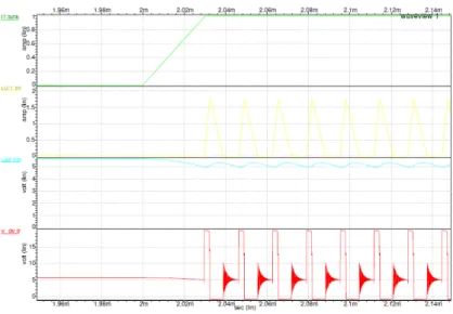
Figure 2.8:Normal mode waveform
Fig. 2.8 shows regulator waveforms in normal operation when the output current changes from 0 to 1A. The first row is the output current, the second is the current flowing in the inductor, the third is the output voltage (VOU T in
Fig. 2.6) and the forth is the LX voltage (see Fig. 2.6).
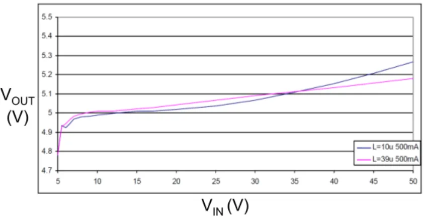
As far as simulated performance is concerned, Fig. 2.9 and 2.10 show the simulations of the variation of the output voltage versus the input voltage (in the range 5 − 50V with different inductors (10µH and 39µH) and for different
output currents (100mA and 500mA).
V
IN(V)
V
OUT(V)
Figure 2.9: VOU T vs VIN with 100mA output current
V
IN(V)
V
OUT(V)
Figure 2.10:VOU T vs VIN with 500mA output current
Fig. 2.11 and 2.12 show the simulations of the load regulation of the regu-lator. More in detail, in Fig. 2.11 the supply voltage is 5V and the regulator goes in dropout mode, keeping the PMOS always on, while in Fig. 2.12 the supply voltage is 12V, like in typical condition.
2.3 Validation: simulations and measurements
Load Regulation 5V
4.7 4.75 4.8 4.85 4.9 4.95 5 0.1 0.2 0.3 0.4 0.5 IoutV
OUT(V)
I
OUT(A)
Figure 2.11:Load Regulation with 5V supply voltage
Load Regulation 12V
4.9 4.95 5 5.05 5.1 0.1 0.2 0.3 0.4 0.5 IoutV
OUT(V)
I
OUT(A)
3 Drivers for inductive loads
Especially in the automotive environment, the use of electromagnetic actu-ators, like injectors, relays and solenoid electro-valve, is constantly increasing, driven by the continuous replacement of mechanical parts with electronics ac-tuators.
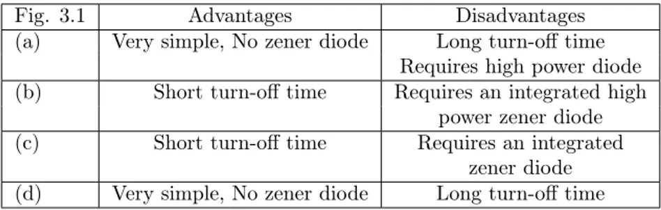
This exchange on one hand permits to control electronically the engine and the other mechanical parts of the car, reducing the fuel consumption and the CO2 emissions, but on the other hand requires electronic driver for such kind of loads, having an inductive behavior. Indeed, compared with classical drivers for resistive and capacitive loads, the design of drivers for inductive loads, requires overcoming more issues because the management of the current, and then the energy stored in the inductor, must be well considered[26, 27, 28, 29]. In fact, when inductive loads are driven, it’s very important controlling the freewheel-ing phase. As shown in [30], there are 4 main freewheelfreewheel-ing strategies proposed in literature that can be used, explained in Fig. 3.1. Table 3.1 shows both the advantages and disadvantages of all those different freewheeling strategies.
L L
(a) (b) (c) (d)
L L
Figure 3.1:Principles of typical solutions to handle inductive freewheeling
Actually those drivers should be part of distributed systems interconnected by digital controllers with different busses.
This kind of approach leads the IC manufactures to integrate on the same die the power devices with the interface to the digital control host through standard local communication protocols, like Serial Peripheral Interface (SPI) or Inter-Integrated Circuit (I2C), and/or through vehicle networks, like FlexRay, CAN or LIN busses.
At the same time, to guarantee the latest functional safety standards that can be found in automotive grade devices, like ISO26262, it’s necessary to integrate on the same die also diagnostic circuits that monitor constantly the status of the driver and signal to the digital part when a fail condition occurs.
Table 3.1: Advantages/Disadvantages of typical solutions in Fig. 3.1
Fig. 3.1 Advantages Disadvantages
(a) Very simple, No zener diode Long turn-off time Requires high power diode (b) Short turn-off time Requires an integrated high
power zener diode
(c) Short turn-off time Requires an integrated
zener diode (d) Very simple, No zener diode Long turn-off time
The first freewheeling strategy, shown in Fig. 3.1(a), is normally used when a constant current flow is needed, like in a buck DC-DC converter and in a Lun-dell alternator as excitation driver[31]. Indeed, this configuration has a very long turn-off time and, acting the MOSFET with a PWM like signal, permits to maintain a constant current flow in the inductor.
The second and third freewheeling strategies, shown in Fig. 3.1(b) and (c), are normally used when the current must be zero at the end of the operation, like acting a relay or a solenoid valve. In fact, in this case, is very important to discharge the energy stored in the inductor as short as possible, to minimize the turn-off time,ensuring a good system behavior.
The last freewheeling strategy, shown in 3.1(d), has the same behavior of 3.1(a), but can be used only with low currents, because of the higher power dissipation in the freewheeling phase.
3.1 Solenoid Valve Driver
will be exploited.
Section 3.1 shows the development of an inductive load driver, highlighting the design and validation phases, especially suited to drive relays and solenoid valves with integrated capability of self-monitoring and fault diagnostic. It has been designed to overcome the limitations of the circuits on Fig. 3.1 (c) and (d), combining the main advantages of the two structures and avoiding the in-tegration of power diodes or power zeners as in the solution (a) and (d) in Table 3.1 and Fig. 3.1. The designed smart driver can be easily integrated as hard macro-cell in more complex automotive grade ICs and can be directly inter-faced to a host digital ECU since it integrates both the High-Voltage (HV) MOS power circuitry and the low-voltage circuitry for control and digital interfacing.
Section 3.2 presents the design and validation phases of a single-chip integrated Rotor Coil Driver that can be used in automotive alternators. It integrates the power switch with the control circuitry and the diagnostics. It follows the freewheeling strategy shown in 3.1(a),with new functionalities, like full reverse polarity protection and programmable output slope control against in-rush cur-rents and current spike transients. This rotor coil driver has been implemented in a 0.35µm HV-CMOS technology and has been embedded in a mechatronic brush-holder regulator system-on-chip for an automotive alternator.
3.1 Solenoid Valve Driver
The inductive load driver, implemented in 0.35µm HV-CMOS IC technology from Austriamicrosystems, fulfills all the requirements that can be found in automotive grade devices. The smart driver has been designed to be integrated as hard IP in automotive UCs and it communicates with the digital part into the IC, receiving the command signal and sending back the status flags.
3.1.1 Design
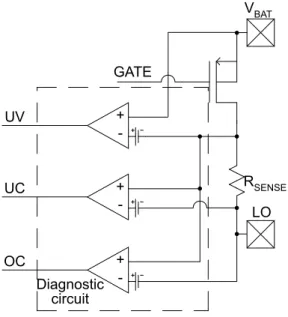
The scheme of the driver, shown in Fig. 3.2, can be divided into 4 different blocks: the power MOS driver, the gate-driver, the zener-like circuit, detailed in Fig. 3.3, and the diagnostic circuit, detailed in Fig. 3.4.
Gate
driver
Zener-like
circuit
Diagnostic
circuit
UC OC UV HS_ON VBAT LO RSENSE GATEFigure 3.2: Inductive driver block diagram
The driver is an integrated high-power high-side PMOS with low ON resis-tance. The gate-driver block drives the gate of the PMOS power switch to turn it ON and OFF depending on the status of the HS_ON digital signal in Fig. 3.2. The zener-like circuit is the active circuit that turns ON the PMOS during the freewheeling phase. The scheme diagram of this block is shown in Fig. 3.3. With respect to state of art solutions in Fig. 3.1 and Table 3.1, this different approach (configuration of Fig. 3.2 with a zener-like circuit as in Fig. 3.3) avoids the use of power diodes, occupying a large part of the chip area, as is in Fig. 3.1(a) or (b) and avoids the use of integrated zener diodes as in Fig. 3.1(b) or (c).
tech-3.1 Solenoid Valve Driver
Zener-like
circuit
M2 LO VBATGate
driver
M3 GATE M1 M4 M5 VON HS_ON VCL1 HS_ONFigure 3.3:Gate-driver and Zener-like circuits
nology and in other typical HV-CMOS technologies.
Some BCD technology exists, offering the integration of zener diodes, but as process option at an increased technology and integration cost vs. basic HV-MOS technologies.
The gate-driver is the block that drives the gate of the PMOS power switch to turn it ON and OFF depending on the status of the HS_ON digital signal in Figs. 3.2 and 3.3[32]. The PMOS M4 and the VON bandgap stabilized voltage
reference, generated according Equation (3.1) while VGSM AX(M 1) is the
maxi-mum VGSfor M1 and V Tp(M 4)is the threshold voltage of the PMOS M4, limit
the VGS of the PMOS M1 below the maximum allowed for that device.
VON = |VGSM AX(M 1)| + |V Tp(M 4)| (3.1)
The main part of the zener-like circuit is the NMOS M2 that is turned ON when the voltage on the output is below ground. In this condition the PMOS M1 works in saturation region and the VGS must follow the Equation (3.2)
the PMOS transistor. |VGSON| = |V Tp| + s 2IL βp (3.2) VCL= |VCL1| + V Tn(M 2) (3.3)
Absolute values are used for VGSON and V Tp in Equations (3.2) and (3.3)
since for a PMOS these values are negative. Similarly VCL is negative;
Equa-tion (3.3) gives the absolute value of VCL below ground.
The diagnostic circuit, shown in Fig. 3.4, is composed by an under-voltage (UV) comparator on the output, by a current limitation circuit and by an overcurrent (OC) and undercurrent (UC) comparators.
UV + -UC + -OC + -Diagnostic circuit RSENSE LO VBAT GATE
Figure 3.4:Diagnostic circuit
The under-voltage comparator senses the difference between the battery pin and the output pin. If this difference is higher than a fixed threshold (about 2V), it sets the UV flag.
3.1 Solenoid Valve Driver
The current limitation circuit, on the other hand, senses the current flowing in the power PMOS using a very small sensing resistor(RSEN SE) and uses this
information to limit the current flowing in the driver. Moreover it uses the information coming from the sensing resistor to compare the PMOS current with two fixed thresholds and then to generate an undercurrent (UC) and an overcurrent (OC) flags.
All those thresholds (under-voltage, undercurrent and overcurrent) are gener-ated by a bandgap stabilized voltage reference circuit placed far away from the power devices, to limit the thermal interferences between the two circuits.
The UC flag permits to detect a disconnection of the load while the OC flag permits to detect a short circuit condition on the load. The OC flag, after a confirmation time of 1ms, forces the turn-off of the driver to avoid damage to the driver itself. This solution can be not sufficient if a short circuit condition with a very low ohmic path is present. In this case the current flowing in the driver is limited only by the sensing resistor and the inductor series resistor and it can reach several amperes, damaging metal routing of the driver. To avoid this condition, the circuit uses the information on the current, sensed through RSEN SEin Fig. 3.4, as feedback to limit the maximum current flowing in the
driver. To be noted that the current limitation circuit and the OC flag circuit share the same current sensing device and the same threshold generation unit. This solution ensures that the OC flag is always set when the current is limited, also in worst-case condition.
As said before, the driver, although is designed to drive inductive loads, imple-ments also a linear current limitation circuit, permitting to drive also resistive and capacitive loads. In fact, the main issue, when a capacitive load is driven, is the very high in-rush current that charges the load capacitor. This very high current can destroy the driver if a current limitation circuit is not present.
Implementing in the same smart driver both the zener-like integrated circuit and the current limitation circuit permits to connect inductive, resistive and capacitive loads using the same driver.
Moreover to protect the circuit, an integrated temperature sensor and an over-temperature protection have been implemented. When the die over-temperature reaches the over-temperature threshold, the driver is automatically turned-off and kept in this state until the die temperature fall below the recovery thresh-old.
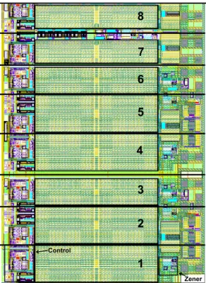
3.1.2 Layout
To check the design of the inductive load, a testchip has been realized, inte-grating on the same die eight drivers with different maximum operating current together with a power management block and with CAN and LIN transceivers for interfacing versus an off-chip network or control host.
1
2
3
4
5
6
7
8
Zener ControlFigure 3.5:Layout of 8 different inductive drivers
3.1 Solenoid Valve Driver
are of Type1, with 600mA as maximum DC current, the drivers 3 and 6 are of Type2, with 400mA as maximum DC current and the drivers 7 and 8 are of Type3, with only 200mA as maximum DC current.
The drivers 1, 2, 4 and 5, sustaining higher currents are those occupying a larger area rather than drivers of Types 2 and 3.
Besides, Fig. 3.5 highlights the layout of control logic and of the zener-like circuits for the first driver.
Table 3.2 summarizes the operating temperature, voltage and current ranges of the driver. Moreover, Table 3.2 shows the typical ON resistance of the three dif-ferent drivers, the value of the diagnostic thresholds and the maximum driving current in DC conditions and AC pulsed ones.
Table 3.2: Operating and environmental ratings
Operating temperature -40 − 150 ◦C
Operating battery voltage (VBAT) 5 − 40 V
DC current Type1 Up to 0.6 A
Pulsed current Type1 Up to 1.1 A
DC current Type2 Up to 0.4 A
Pulsed current Type2 Up to 0.75 A
DC current Type3 Up to 0.2 A
Pulsed current Type3 Up to 0.58 A
PMOS ON resistance (Type1) 330 mΩ
PMOS ON resistance (Type2) 470 mΩ
PMOS ON resistance (Type3) 625 mΩ
UV flag detector 2 V
UC flag detector 20 mA
OC flag detector (Type1) 830 mA
OC flag detector (Type2) 580 mA
OC flag detector (Type3) 435 mA
Zener activation voltage (referred to ground) -15 V
3.1.3 Quality and safety aspects
As said in the introduction (Chapter 1), to achieve the stringent require-ments of the ISO26262 standard, many diagnostic features must be integrated
on the same die, in order to detect a failure condition and, when it is possible, to take countermeasures to isolate the fault, avoiding hazard conditions. In fact, ISO26262 requires to monitor continuously the devices, signaling to the driver when something is not working correctly.
In this case, the diagnostic block is in charge to detect the status of the driver and the digital part, using the control and status flags (HS_ON, UV, UC and OC), can detect failure conditions, like the disconnection of the load or the short to ground of the driver. Moreover, the digital part can also detect a vari-ation of the parameters of the driver, like the ON resistance, and can implement all necessary measures to avoid hazard conditions.
3.1.4 Validation
To validate the design of the inductive load driver, the driver has been first simulated and then measured. Hereafter the simulation and measure results will be discussed.
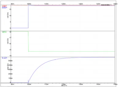
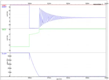
Figure 3.6:Simulated turn-on transient
tran-3.1 Solenoid Valve Driver
Figure 3.7: Simulated turn-off transient
sients of the driver in the example case of three inductive loads of 600mH each, connected in parallel between the pin LO and ground.
The waveform at the top of each figure highlights the battery (red line) and the LO (blue line) voltage signals.
The waveform in the middle shows the voltage on the gate of the driver PMOS. The waveform at the bottom shows the current IL flowing in the inductor.
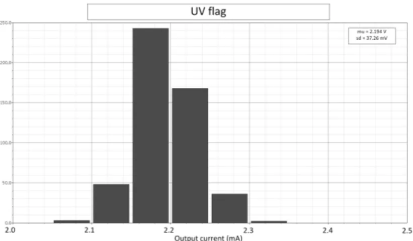
Figs. 3.8, 3.9 and 3.10 shows respectively the results of the Montecarlo simula-tion of the under-voltage (UV), undercurrent (UC) and overcurrent (OC) flags. Those Montecarlo simulations are done considering both process and mismatch variations.
Figure 3.8:UV flag Montecarlo simulation
3.1 Solenoid Valve Driver
Figs. 3.11 and 3.12 shows respectively the oscilloscope waveforms of the turn-on and turn-off transients with the same load condition of Figs. 3.6 and 3.7.
In this case the yellow waveform is the battery voltage, the red is the LO voltage and the green is the current flowing in the load.
Figure 3.11:Measured turn-on transient
3.1 Solenoid Valve Driver
In the Fig. 3.12, it is possible to note that the negative clamping voltage is only 1.5V below ground, instead 15V as designed. This behavior has been analyzed and the root cause was found in a parasitic BJT not included in the models supplied by the foundry. In fact, a parasitic npn bipolar transistor (shown in Fig. 3.13), generated by two HV-MOS devices in the VCL1generator
in the Fig. 3.2, reduces the clamping voltages to the measured value.
N-well N-well
P-substrate
Figure 3.13:npn BJT parasitic device
To solve this issue, a new silicon fab run is necessary to increase the distance between the n-wells and increase the immunity of the VCL1 clamp generator to
this kind of parasitic devices.
Figure 3.14:Measured UV flag
Figure 3.14 shows the UV flag waveform. In this case, the battery voltage (the yellow line) is kept to 10V, while the LO pin (the red line) is swept from
10V to ground and vice-versa.
To avoid a very high current flow through the driver, it has been kept off during the measurement.
The green line is the resulting diagnostic flag: it is set when the difference is higher than 2.2V, and is cleared when it becomes lower.
Figure 3.15:Measured UC flag
Figure 3.15 shows the UC flag waveform. In this case, the battery voltage (the yellow line) is kept to 10V, while from the LO pin (the red line) is sunk a variable current (the blue line) from 120mA to 0mA and vice-versa.
In this case, to ensure the right behavior, the driver is kept on during the test. The green line is the resulting diagnostic flag: it is set when the current is below 20mA, and is cleared when it becomes higher.
3.2 Rotor Coil Driver
3.2 Rotor Coil Driver
The Rotor Coil Driver (RCD), implemented in Austriamicrosystems HV-CMOS 0.35µm ASIC technology, has been designed to completely fulfill the requirements that can be found in automotive grade devices. Particularly the RCD can operate with battery voltage between 6V and 50V, covering both cold cranking and load dump events. Furthermore it can sustain permanent reverse polarity on battery down to -3.2V, which is the maximum forward volt-age across the series of two diodes in the stator rectifier bridge, and unexpected battery voltage surges up to 55V.
The RCD has been designed to operate correctly up to the max absolute junc-tion temperature of 180◦C before reaching an “over-temperature protection threshold”, indeed above 180◦C the integrated temperature protection circuit switches off the driver to avoid silicon damage.
This RCD, respect to other solutions [33, 34], implements a current slope con-trol on the high-side, avoiding voltage spikes due to parasitic inductance of the alternator-battery cable.
+
-Rotor coil I1 I2 I3 VBAT VL + -RCDFigure 3.16:Connection of alternator output, battery and rotor coil with its driver
In fact, in Fig. 3.16 the current that flows from the rectifier bridge (I1) is
almost constant and depends on the magnetic field on the stator coils and hence on the rotor coil current. During the turn-on phase, if the current I3 increases
very rapidly, according to Eq. (3.4) the current I2 will decrease rapidly as
consequence. According to Eq. 3.5, due to the parasitic inductance of the wire LW, there will be a fast negative voltage spike on VBAT. During the turn-off
phase a dual condition happens: if the current I3 decreases rapidly, I2 will
increase rapidly as consequence and a fast positive voltage spike on VBAT can be observed. Those spikes are not acceptable because they can generate EMI problems to other electronic devices.
∆I1= ∆I2+ ∆I3 since ∆I1' 0 → ∆I2' ∆I3 (3.4)
VL= LW ∂I2 ∂t = −LW ∂I3 ∂t (3.5)
3.2.1 Design
The coil driver scheme, shown in Fig. 3.17, can be divided into 4 different blocks: the smart gate driver, the power switch, the current sensing and the ADC and monitors.
The interface towards the processing core of the voltage regulator system is composed by the following output signal: two flags, OPEN and SHORT, sig-naling if the current in the rotor coil is under or over programmable current thresholds and a 10-bit signal providing a measure of the rotor coil current. The digital core sends to the smart gate driver in Fig. 3.17 the order to increase or decrease the rotor coil current changing the duty cycle of the EXC_CT RL control signal.
The gate of the high side switch is driven by a PWM signal with a fixed frequency fP W M in a range of some hundreds of Hz typically. Rotor current is
modulated changing the duty cycle of the PWM signal from minimum, typically set to 5%, to 100%(maximum field).
Fast transients in the current sunk from the battery can generate undesired overshoots, oscillations and ringing on the battery voltage. To avoid them, for EMC compliance, the current through the high-side has a slope controlled transient during the switching on and off transitions. The digital core, through the SLP _CT RL signal, can select the desired current slope.
3.2 Rotor Coil Driver POWER SWITCH SMART GATE DRIVER ADC SAR 10-bit Rotor monitor 10 OPEN SHORT ADC and MONITORS CURRENT SENSING EXC & SLP _CTRL SMART GATE DRIVER VBAT EXC
Figure 3.17:Alternator coil driver schematic
Power Switch
One of the most important blocks is the high-side power switch, which is a p-type HV lateral diffused (LD) MOS with 3.3V thin gate oxide, included in the HV-CMOS technology from Austriamicrosystems (H35). The main operating and absolute parameters of the HV-PMOS power switch are shown in Table 3.3, which also shows a comparison with the lateral diffused HV-NMOS of the same technology.
Both PMOS and NMOS HV devices fulfill the operating battery range, but the choice of PMOS is due to two main factors: reverse polarity protection and charge pump avoidance. Using the PMOS is possible, driving the bulk terminal properly, to avoid current flow in parasitic devices when the battery voltage is below zero, as shown in Fig. 3.18. Using the NMOS as in [33, 34] that behavior cannot be achieved using a standard HV-CMOS technology, but a more expensive technology must be used to avoid the diode between drain and substrate.
Table 3.3: HV-PMOS and HV-NMOS operating and absolute ratings HV-PMOS HV-NMOS Operating Junction -40◦C to 150◦C -40◦C to 150◦C Temperature Absolute Junction -40◦C to 180◦C -40◦C to 180◦C Temperature Maximum Drain-Source -50V / -55V 50V / 55V
Voltage (operating / absolute)
Maximum Drain-Source -70V 70V
Breakdown Voltage
Maximum Gate-Source -3.6V / -5V 3.6V / 5V
Voltage (operating / absolute)
ON Resistance 1.3Rn Rn
not needed. Indeed, the gate capacitance of the switch is in the order of some nF and is almost the same when a PMOS or an NMOS is used, so the charge pump for gate driving requires big integrated capacitors. In fact, considering that in the alternator system additional pins for external bypass capacitors are not provided, integrated capacitors must be used. If a rise time of about 10µs is considered, they have to be in the range of 100pF, requiring a lot of silicon area. Considering also that in the chosen HV-CMOS technology the RDSon of
the HV-PMOS is not much higher than the NMOS one, as shown in Table 3.3, the use of NMOS with big capacitors for the charge pump could have an higher die size and silicon cost than the use of PMOS. Avoiding charge pump circuitry permits also to reduce the EMC conducted emissions and simplify the driving circuitry, because no advanced techniques, like spread spectrum, are necessary to reduce EMI in charge pump design. Basing on the previous considerations, in the considered HV-CMOS technology, the use of PMOS instead of NMOS permits to reduce the total area occupation and then the silicon cost, permits to achieve full reverse polarity protection and also permits to have better per-formances in terms of EMC radiated and conducted noise.
As far as EMC is concerned, in addition to current slope control and the avoidance of charge pump circuitry, EMC decoupling capacitors have been implemented on the supply of clocked blocks in the RCD (e.g. the SAR ADC).
3.2 Rotor Coil Driver VBAT EXC VBAT EXC VSB VSD p+ n+ p+ p+ Gate N-WELL P-SUBSTRATE P-WELL Drain Sub Source Bulk HV-PMOS p+ p+ n+ n+ Gate N-WELL P-SUBSTRATE P-WELL Drain Sub Source Bulk HV-NMOS DSB DSD
Figure 3.18:PMOS vs. NMOS comparison during reverse battery condition
To avoid crosstalk between different blocks due to shared supply lines, a layout design strategy with dedicated metal routing for supply and ground has been implemented.
Smart Gate-Driver
The smart gate driver is the block that drives the gate of the PMOS power switch in Figs. 3.17 and 3.19 to obtain the rotor coil current control. Fig. 3.19 highlights this block (the power MOS is the device M1) which operates in two different modes, one during the turn-on and turn-off transients (switch S1 in Fig. 3.19 in position 3), and one during the on and off steady states (switch S1 in Fig. 3.19 in positions 2 and 1, respectively). When the turn-on command is received through the EXC_CT RL control signal, the gate driver unit starts driving the gate of M1 in order to have a slope-controlled current flowing in the
PMOS. The switch S1 is closed in position 3, connecting together the gates of the two PMOS (M1 and M2). The digital controlled current ramp generator in Fig. 3.19 starts generating a current ramp on the OUT pin. Because M1 and M2 act as a current mirror, a current ramp on M2 forces a current ramp also in M1. The current that flows in M1 is obtained by scaling the current that flows in M2 by the dimensional factor ratio of the two PMOS devices, KM 1M 2,
which amounts to about 1600. The slope can be changed in two different ways: setting high the SLP _CT RL signal doubles the slope and adjusting the bias current in the gate driver permits a finest selection of the output current slope. In this coil driver both of those strategies are implemented: for the bias current both temperature coefficient and absolute value can be trimmed; trough the SLP _CT RL signal the slope can be set to the trimmed value or to the double.
VBAT EXC GATE-DRIVER M1 D1 EXC_CTRL SLP_CTRL IM1 Bias current ID1 M2 Digital controlled current ramp generator VSGMAX VSGSEL S1 OUT 1 2 3
Figure 3.19:Gate-Driver block diagram
As consequence, as reported in Eq. (3.6), by controlling during turn-on and turn-off transients the shape and slope of the Iout signal, which is limited at a
3.2 Rotor Coil Driver
coil current IM1, which is in the order of several Amperes. Since IM 1 in Fig.
3.19 is the rotor coil current, the control of the slope of that current realized by the proposed gate driver allows avoiding overvoltage phenomena and spike generation due to too fast current slope.
IM 1 = KM 1M 2∗ IM 2= KM 1M 2∗ IOU T (3.6)
On the other hand the slope of the current IM 1 cannot be too slow. This
is because during the turn-on and turn-off transients, when the rotor current is flowing in D1 and M1, like shown in Fig. 3.20, the PMOS works in satura-tion region and large tON/tOF F values would lead to high energy dissipation.
During transients the output voltage and current of the PMOS M1 are both different from 0: the current IM 1 can be modeled as a ramp going from 0 to
IM AX (when turning-on, the opposite when turning-off), while the M1 output
voltage is almost constant, clamped at VSD= VBAT-VEXC=VBAT+VDIODE
since D1 is on. As consequence the energy dissipated at each switching tran-sient can be modeled as in Eq. (3.7). The average power dissipation PDAV G,
with a PWM switching frequency fP W M, can be modeled as in Eq. (3.8).
EDON = tON∗
(VSD∗ IM AX)
2 , EDOF F = tOF F ∗
(VSD∗ IM AX)
2 (3.7)
PDAV G= fP W M ∗ (EDON + EEOF F) (3.8)
For typical values of VBAT = 14V, VDIODE = 1V, IM AX = 5A, fP W M =
250Hz, and a current slope controlled at 200mA/µs (slow control set of the RCD), tON and tOF F amount to 25µs. Therefore EDON and EDOF F are
al-ways less than 1mJ and PDAV Gis less than 0.5W. In the worst case scenario of
IM AX = 8A and VBAT = 50V then PDAV Gis about 4W, which can be reduced
to 2W using a faster slope control at 400mA/µs (fast control set of the RCD). The PDAV G contribution should be added to the power dissipation when the
PMOS is on, due to non null RDSon resistance: PDON = D ∗ RDSon∗ IM AX2
IM AX = 5A and RDSon = 60mΩ and worst case values of IM AX = 8A and
RDSon= 100mΩ then PDON is up to 1.5W and 6.4W respectively. The RCD
power stage has been designed so that such power dissipation values can be sustained.
From the above case example is clear that, by proper controlling the current slope in the range of hundreds of mA/µs, the main contribution to power dissi-pation is due to PDON. On the contrary, if the current slope is not controlled,
and is in the range of tens of mA/µs, then the above PDAV G power
dissi-pation becomes the dominating contribution reaching critical values for the HV-PMOS.
ID1
IM1
DIODE ON TURN-ON transient PMOS ON TURN-OFF transient DIODE ON
VEXC 0 VDIODE=-1 VBAT tON tOFF 0 IMAX
Figure 3.20:Gate-Driver transients
After analyzing the behavior of the smart gate driver during transients, here-after its configuration during on and off steady states is discussed. During the on steady state to lower the RDSon and minimize the power dissipation, the
switch S1 in Fig. 3.19 is closed in position 2, connecting the output of the gate driver to VSGM AX and forcing the maximum allowed VSG to lower the RDSon
resistance of the PMOS. To be noted that the gate driver is supplied between VBATand ground, but its output is limited between VBATand VBAT−VSGM AX,
3.2 Rotor Coil Driver
3.5V from V BAT. Since VSGM AX has been generated using a bandgap circuit
its value is stable in a wide temperature range and is always within the maxi-mum operating value of 3.6V reported in Table 3.3. During the off steady state the switch S1 in Fig. 3.19 is closed in position 1 and the output of the gate driver is VBAT forcing the HV-PMOS off (VSG= VSGM IN = 0).
Current Sensing and Monitors
The current sensing block in Fig. 3.21 is in charge to read back the current flowing in the switch and to send this information to the digital part[35]. More-over it informs the digital part if a fail status is reached. It sends to the digital part two diagnostic flags: the OPEN flag is set when the coil current is below a fixed threshold (about 20mA) to inform that the rotor coil is disconnected and the SHORT flag is set when the current is higher than the maximum allowed current (programmable between 8.5 to 12A) to detect fast current spikes, e.g. due to a short on the rotor coil windings. The used ADC is a 10-bit successive approximation converter (SAR) with a main clock of 704kHz and a sample rate of 64kHz. Such frequencies allow for fine time resolution of the alternator regulator as foreseen in recent works [33, 34]. A complete block diagram of this block is shown in Fig. 3.21.
The VT H1 and VT H2 thresholds are calculated following the Eqs. (3.9) and
(3.10).
VT H1= Rf∗ IT H1; IT H1= 0.02mA (3.9)
VT H2= Rf∗ IT H2; 8.5A < IT H1< 12A (3.10)
An integrated temperature sensor is also present forcing in off state the power switch when the measured temperature value is beyond a programmable threshold.
Moreover the reference current used in the ADC is temperature stabilized since it is generated as the sum of a PTAT (proportional to absolute temperature) current and of a CTAT (complementary to absolute temperature) current. A
ADC and MONITORS 10-bit ADC IN VREF+ VREF-OUT 3.3V 10 VCURR VTH1 VTH2 OC UC R esi st or ba se d C urre nt Se nsi ng VBAT EXC M1 D1 VCURR=RF*IM1 IM1
Figure 3.21:ADC and monitors block diagram
trimming structure on the overcurrent detector and a software calibration on the output of the ADC have been also implemented. Particularly, during the calibration phase, a fixed current is imposed on the rotor coil and the same current is acquired through the ADC. Doing the calibration with two different current values is possible to compensate the offset and gain error of the ADC.
3.2.2 Layout
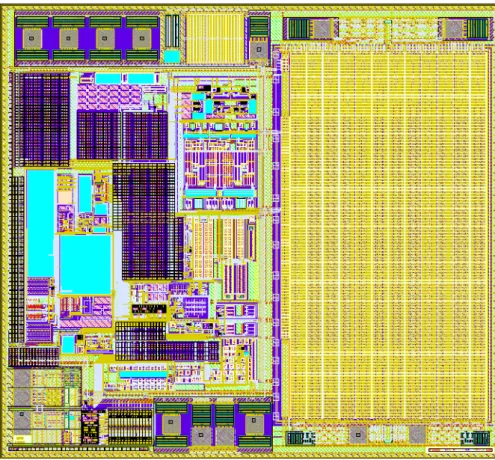
The Rotor Coil Driver has been realized in 0.35µm HV-CMOS technology and integrated in an alternator voltage regulator.
Fig. 3.22 shows the layout of the complete voltage regulator IC (see Chapter 5) and highlights the PMOS, diode and control logic placing. Table 3.4 high-lights the area contribution of the RCD, 29% of the total regulator area. The main contribution is due to the HV-PMOS and diode, see Fig. 3.22, which are 16% and 10% of the total regulator while the low-voltage control logic occupation is limited to about 3%.
Table 3.5 shows the electrical and environmental operating and absolute ranges of the RCD, determined by design choices and verified by experimental
3.2 Rotor Coil Driver
!
Figure 3.22:Alternator Voltage Regulator IC with the designed rotor coil driver
measurements on realized IC samples.
3.2.3 Quality and safety aspects
It is worth nothing that to meet "zero defect" automotive requirements in the design phase it has been verified that every device in the RCD is working in the safe operating area with the lifetime acceleration factor close to 1 in order to increase the Mean Time To Failure (MTF). As already discussed before, ESD, EMC and on-chip diagnostic and protection issues have been addressed and