UNIVERSITÀ DEGLI STUDI DI ROMA
"TOR VERGATA"
FACOLTA' DI SCIENZE MATEMATICHE FISICHE E NATURALI
DOTTORATO DI RICERCA IN
MATERIALI PER L'AMBIENTE E L'ENERGIA
CICLO DEL CORSO DI DOTTORATO
XII
Thin films growth by Pulsed Laser Deposition for Solid Oxide Fuel Cell
applications
Simone Sanna
A.A. 2009/2010
Docente Guida/Tutor: Dr. Antonello Tebano, Prof. Giuseppe Balestrino
Coordinatore: Prof. ssa Silvia Licoccia
di film sottile. Vale a dire, negli ultimi anni molti ricercatori stanno lavorando per realizzare le celle a combustibile Ossidi solidi in scala micrometrica (micro-SOFC). Le micro celle a ossidi solidi sono molto promettenti, in quanto una riduzione su scala micrometrica dello spessore dei componenti delle celle a combustibile (catodi, elettroliti e anodi) comporta un aumento considerevole delle prestazioni. Prestazioni più elevate del SOFCs consente di ridurre la
temperatura di esercizio (circa 800-1000°C per SOFC convenzionali basate su zirconia stabilizzata con yttria (YSZ)) tali da consentire il loro uso come batterie per i dispositivi portatili. Dispositivi elettrochimici possono essere miniaturizzati per applicazioni portatili (µ-SOFC), utilizzando nuove tecniche di deposizione di film sottili. Una delle tecniche più promettenti è la Pulsed Laser
Deposition (PLD). Questa tecnica è adatta a crescere ossidi complessi e eterostrutture con spessore complessivo di pochi nanometri. In questa tesi abbiamo utilizzato la tecnica PLD per la
fabbricazione di componenti SOFC, come elettroliti e catodi. La qualità cristallina e la struttura morfologica dei film sottili sono state studiate con la diffrazione a raggi X (XRD) e con il Field Emission Scanning Electron Microscopy (FE-SEM). In conclusione, le prestazioni dei componenti sono stati studiati con la Spetettroscopia di Impedenza ad alta e bassa pressione parziale di
ossigeno nell’inervallo di temperature che vanno da 400°C a 800°C.
Capitolo 1 è incentrato sullo stato dell'arte delle tecnologie a film sottile in µ-SOFC.
Capitolo 2 spiega le tecniche utilizzate per la sintesi e la caratterizzazione elettrochimica di film sottili e di eterostrutture.
Capitolo 3 mostra le proprietà della Ceria drogata con Samario (SDC) sotto forma di film depositato su MgO (001).
Capitolo 4 illustra i meccanismi di conducibilità ionica all'interfaccia SDC/YSZ di film superreticoli depositati su MgO.
Outline
i
Chapter 1
Overview
1.1 Solid Oxide Fuel Cells description 1
1.2 Micro-SOFC 3
1.3 Ionic conductivity in ultra thin films and heterostructures 5
Chapter 2
Fabrication and characterization of thin films for
SOFC applications
2.1 Fundamentals of Pulsed Laser deposition 18
Spectroscopy (EIS) 25
2.5 defects in oxides 29
2.6 Experimental setup for EIS 32
Chapter 3
Structural and electrochemical characterization of
epitaxial Samarium-doped ceria thin film
3.1 Introduction 36
3.2 Epitaxial thin films and heterostructures deposited
onto single crystal perovskite substrates 37 3.3 XRD characterization of SDC and SDC/STO deposited
onto MgO (001) single crystal substrate 43 3.4 Morphological characterization of SDC/MgO (001)
and SDC/STO/MgO (001) 49
3.5 Electrochemical characterization of SDC/STO/MgO (001) 54
[SDC/YSZ] heterostructures
4.1 Introduction 66
4.2 Heterostructures and superlattices 67
4.3 XRD characterization 71
4.4 Electrochemical Impedance characterization of (YSZ/SDC)N
superlattices 74
4.5 X-Ray reciprocal space mapping of (YSZ/SDC)N heterostructures 79
4.6 Conclusions 81
Chapter 5
Nanostructured cathode thin films grown by Pulsed
laser deposition
5.1 Introduction 84
5.2 Thin films deposited on polycrystalline substrates
5.5 Conclusion 102
Conclusion
106Outline
The growing demand for miniaturized systems for energy conversion and storage has prompted extensive research aimed at the fabrication of solid state ionic devices in thin film form. Namely, in the recent years many researchers are working to realize Solid Oxides Fuel Cell in micrometric scale (micro-SOFCs). Micro-SOFCs are very promising because a reduction to the micro-scale of the fuel cell components (cathodes, electrolytes and anodes) thickness has relevant consequence to increase the performances. Higher performance of the SOFCs means to reduce the working temperature (about 800-1000 °C for conventional SOFC based on yttria-stabilized zirconia) allowing their use as batteries in the portable devices. Electrochemical devices can be miniaturized for portable applications (µ-SOFCs) using novel deposition techniques of thin films and heterostructures. One of the promising
ii
grow complex oxides and heterostructures with overall thickness of few nanometers. In this thesis we used the PLD technique for the fabrication of SOFC components, such as electrolytes and cathodes. The crystalline quality and the morphological structure of the thin films were investigated by X-Ray Diffraction (XRD) and Field Emission Scanning Electron Microscopy (FE-SEM). In conclusion the performances of the components were studied using Electrochemical Impedance technique at high and low oxygen partial pressure in the temperature range from 400°C to 800°C. Chapter 1 is focused on state of the art of thin film technologies in the µ-SOFCs. Chapter 2 explains the techniques used for the synthesis and the electrochemical characterization of the thin films and the heterostructures.
Chapter 3 shows the properties of the epitaxial Samarium-doped Ceria (SDC) thin film with lower and higher mosaic spread deposited onto MgO (001) single crystals. Chapter 4 shows the ionic mechanisms of the conductivity at the interface in the SDC/YSZ multilayered systems.
Chapter 5 shows the performances of the nano-porus cathodes with larger active surface and larger triple phase boundary (TPB) at the electrode/electrolyte compared to dense cathodes.
Chapter 1
Overview
1.1 Solid Oxide Fuel Cells description
Fuel cells are electrochemical devices that convert the chemical energy of a reaction directly into electrical energy. Fuel cells consist of an electrolyte layer in contact with a porous anode and cathode on either side. A schematic representation of a fuel cell, based on oxygen-ion conductor, with the reactant/product gases and the ion conduction flow directions through the cell is shown in Figure 1. In a typical fuel cell, gaseous fuels are fed continuously to the anode (negative electrode) and an oxidant (i.e., oxygen from air) is fed continuously to the cathode (positive electrode); the electrochemical reactions take place at the electrodes to produce an electric current.
2
Solid oxide fuel cells (SOFCs) are advanced electrochemical reactors operating at high temperature. SOFCs are presently under development for a variety of electric power generation applications with high energy conversion efficiency [1].
Figure 1. Diagram of the SOFC based oxygen-ion conductor.
The main advantages of the SOFC can be summarized as follows: • SOFCs are flexible in the choice of fuel such as carbon-based fuels
• SOFCs have a solid state construction and, as they have no moving parts, can be installed indoors.
• The high operating temperature of SOFCs produces a high quality heat byproduct which can be used for co-generation, or in combined cycle applications.
• SOFCs do not contain noble metals.
• SOFCs have extremely low emissions, eliminating the danger of carbon monoxide in exhaust gases as any CO produced is converted to CO2 at the high operating temperature.
1.2 Micro-SOFCs
Historically, the materials used for SOFC applications are bulk ceramics and thick films (several micrometers). However, recent trends indicate an increasing interest in thin films SOFC components with thickness of a few nanometers. In particular, the researchers are focused on the fabrication of electrolyte thin films to reduce the ohmic resistance. One of the reasons for the interest in micro-SOFCs is to decrease the operating temperature from the range of 800-1000°C to 600-800°C due to nano-scale dimension . These lower operating temperatures enable the use of lower-cost metallic interconnectors, reduce the thermal stress in the SOFC and possibly allow their use as portable power generators in devices such as laptop computers and mobile telephones. Lower temperatures lead to increased electrolyte ohmic resistance, given the thermally activated behavior of ionic transport. This effect, however, can be compensated by decreasing electrolyte thickness [2].
Thin film deposition can be combined with micro-machining techniques in order to realize fuel cells with micrometer dimensions. In fact, thin films can be deposited on insulating substrate and after the deposition it can be etched.
4
Figure 2 shows a sketch of a micro-SOFC with double chamber (one for a fuel and one for air).
Figure 2. Sketch of a micro-SOFC.
Figure 3 shows a FE-SEM micrograph of a prototype of a free standing micro-SOFC deposited on a silicon nitride (SiN) membrane by pulsed laser deposition (PLD). The SiN membrane was etched by reactive ion etching (RIE) [2].
The prototype was made in three steps:
• Sequential deposition of the electrolyte and anode on the SiN membrane without exposure to atmosphere by PLD.
• Etching of the SiN membrane left on the back side of the chip by RIE.
• Deposition of the porous cathode on the back side of the chip at room temperature by PLD.
Figure 3. FE-SEM micrograph of cross section (a.) and surface-views (b.) of micro-SOFC prototype.
1.3 Ionic conductivity in ultra thin films and
heterostructures
Several researchers such as Maier, Kosacki, Tuller etc. are studying the relationship between the thickness and the ionic conductivity of the electrolyte thin films [3-4]. Kosacki, in particular, reported an enhancement in the ionic conductivity of 10 mol% YSZ thin films for a thickness of less than 60 nm deposited on MgO. The enhancement was attributed to a highly conductive interfacial layer at the YSZ and MgO interface.
6
Figure 3. The resistance of YSZ thin films deposited on MgO substrate as a function of the thickness [3-4].
Maier et al studied the electrical behavior of interfacial regions, which often differs from that of bulk due to space charge effects in the superlattice thin films. In fact, Maier and his coworkers extended the space-charge concept as one of the possible origins of a higher conductivity along interfaces in the nano-scaled materials. This effect is confined to lengths in the order of the Debye length
∞ = Λ c F z RT D 2 2 2 ε (1)
where ε is dielectric constant, z is the number of charges on the defect, c∞ is the molar concentration of defect far from the interface, R is the gas constant and F is Faraday constant. Typical Debye length for extrinsic materials is about 10 nm. For
highly doped, such as SDC and YSZ materials the length of d can be neglected. A Structurally disturbed interface region might result an increase of ionic conductivity. Figure 4 shows the space charge region of an oxygen ion conductor with an increased density of mobile ionic charge carriers for a disordered interface region.
Figure 4. Space charge region of an oxygen ion conductor.
Figure 5 shows the parallel ionic conductivity of CaF2/BaF2 heterostructures deposited by molecular beam epitaxy (MBE) on Al2O3 for films with various periods (thickness of single bi-layer) and interfacial densities in the 430-16 nm range with the overall thickness is 500 nm [5]. Maier shows an enhancement of the ionic conductivity from 430 nm to 16 nm. When the period is less than 16 nm he observed a decrease of the ionic conductivity, probably due to the lack of continuity for tiny thicknesses [5].
8
Figure 5. Ionic conductivity of CaF2/BaF2 heterostructures deposited onto Al2O3 from 430 nm to 16 nm [5].
Figure 6 shows the conductivities as a function of the period (thickness of bi-layer) for films of CaF2/BaF2 with overall thickness in the range 430-2 nm.
Electrical conductivity of Gadolinium-doped-ceria (GDC) and Yttria–stabilized Zirconia (YSZ) films have been extensively studied for application in micro-SOFC. Several researchers such as Maier, Gauckler, Ramanathan, Guo and Kosacki investigated microstructural effects, strain effects and space charge effects induced by the substrates.
Azad et al. studied the nanoscale effect on ionic conductivity of GDC/ZrO2
heterostructures deposited onto Al2O3 single crystals [6]. Structural characterization
indicated that microstructural defects such as dislocations exist in the layers as well as at interfaces resulting from the lattice mismatch between two materials (fig.7).
Figure 7. TEM- micrograph of GDC/ZrO2 heterostructure deposited onto Al2O3 [6].
Similar to the fluoride heterolayers such as GDC and ZrO2, the overall oxide ionic
conductivities increase continuously with decreasing individual thickness, while they decrease as the value of individual thickness is reduced below 15 nm. According to Azad et al., this is due to strain effects associated with the thin films compared to the
10
thick films. The maximum increase in conductivity is around one order of magnitude
compared to a single phase polycrystalline Gd: CeO2 bulk or a single-crystal YSZ
film. The authors proposed that such conductivity increase was attributed to effects of microstructural defects, which may increase the solubility of Gd in CeO2 layers or the mobility of the oxygen vacancies. Figure 8 shows the conductivity as a function of the number of layers with individual thickness of 15 nm [6].
Figure 8. Conductivities of single crystal YSZ, and several number of layers at 650K [6].
The drop of conductivity for the sample with sixteen layers is probably due to high crystallographic disorder.
ZrO2-based heterolayer interfaces (YSZ/Lu2O3, YSZ/Sc2O3, ZrO2+CaO and YSZ/Y2O2) were investigated by Korte et al. in Janek’s group [7-9]. They concluded that the large mismatch at the interface plays a fundamental role for the interface conductivity σint.
Their systems with lattice mismatch are dominated by elastic strain: slight dilatative strain in the YSZ/Lu2O3 systems, significant compressive strain in the YSZ/Sc2O3
systems and significant tensile strain for YSZ/Y2O2 heterostructure. The logarithm of vs. the lattices misfits [7] are reported in Figure 9.
Figure 9. Plot of the logarithm of the maximum change σtot/σvol of the total conductivity relative to the bulk conductivity against the mismatch factor fYSZ/Ins [7].
An expression to calculate the ratio between the interface conductivity σint and the bulk conductivity σbulk as a function of the epitaxial strain ∆a/a was proposed:
a a Y RT VM bulk ∆ − ∆ ≅ ⎟⎟ ⎠ ⎞ ⎜⎜ ⎝ ⎛ ν σ σ 1 3 1 ln int (2)
where ∆VM, Y and ν represent the volume of migration of oxygen vacancies, the Young’s modulus and the Poisson’s ratio, respectively [10-12].
12
Figure 10. Structurally disordered interface region.
Interfaces between two different lattices like grain boundaries or phase boundaries can be structurally classified as coherent, semicoherent and incoherent interfaces depending on the degree of the mismatch [9].
• Coherent interface: the ionic mobility can only be affected by residual lattice strain. The activation energy can change for atomic jumps in the strained region at the interface.
• Semicoherent interface: several dislocations are present at the interface region. The lower packing density and strain field produce the ionic migration.
• Incoherent interface: the interface structure is highly disturbed. In such regions, significant lower packing densities and different atomic interactions are present compared to the bulk. The result is higher ionic conductivity than that of semicoherent and incoherent interfaces.
In general, the interfacial transport becomes faster when changing the interfacial structure from coherent to semicoherent and finally incoherent. Figure 11 shows a sketch of the dependence of interface structure and the density of misfit dislocations on lattice mismatch.
Figure 11. Sketch of the dependence of interface structure and the density of misfit dislocations on lattice mismatch.
Recently, the ionic conductivity of SrTiO3/YSZ/SrTiO3 trilayers deposited onto SrTiO3 (STO)single crystal, were investigated by Garcia-Barriocanal et al [13]. They changed the thickness of YSZ from 62 nm to 1 nm maintaining constant (about 10 nm) the thickness of STO layer. They observed an enhancement of the conductivity by two to eight orders of magnitude compared to the conductivity of YSZ bulk. The authors proposed that both the concentration and mobility of carriers are varied owing to direct or indirect effects of strain. However, it is not clear if the colossal conductivity measured by Garcia-Barriocanal is dominated by ion carriers. Namely a significant electronic contribution is reported in the literature for perovskite thin film such as STO [14-15].
14
Figure 12 shows the dependence of the logarithm of the long-range ionic
conductivity of the trilayers reported by Garcia-Barriocanal STO/YSZ/STO versus inverse temperature. The thickness range of the YSZ layer is 1 to 62 nm [13].
Figure 16. Conductivity of the trilayers reported by Garcia-Barriocanal
STO/YSZ/STO [13].
Guo published a comment to Garcia-Barriocanal’s paper: he proposes that the observed enhancement of the conductivity is mostly due to p-type conductivity of STO. Figure 16 shows a Nyquist of the STO substrate at 220°C [16]. Figure 17 shows the Arrhenius plot of the STO substrate and the heterostructures STO/YSZ/STO.
Figure 16. Impedance spectra of STO substrate at 220°C in air [16].
Figure 17. The Arrhenius plot of the STO substrate and the heterostructures STO/YSZ/STO [16].
16
The activation energy for STO and STO/YSZ/STO has the same value: this indicates that that the contribution of the substrate is predominant relative to the superlattices.
References
[1] A. Boudghene Stambouli, E. Traversa, Renewable and Sustainable Energy Reviews 2002 6, 433.
[2] U. P. Muecke, D. Beckel, A. Bernard, A. Bieberle-Hutter, S. Graf, A. Infortuna, P. Muller, J. L. M. Rupp, J. Schneider, and L. J. Gauckler, Adv. Funct. Mater. 2008, 18, 3158.
[3] I. Kosacki, C. M. Rouleau, P. F. Becher, J. Bentley, D. H. Lowndes, Electrochem. Solid State Lett. 2004, 7, A459.
[4] I. Kosacki, C. M. Rouleau, P. F. Becher, J. Bentley, D. H. Lowndes, Solid State Ionics 2005, 176, 1319.
[5] N. Sata, K. Eberman, K. Eberl, J. Maier, Nature 2000, 408, 21/28 DECEMBER.
[6] S. Azad, O. A. Marina, C. M. Wang, L. Saraf, V. Shutthanandan, D. E. McCready, A. El-Azab, J. E. Jaffe, M. H. Engelhard, C. H. F. Peden, and S. Thevuthasanc, Appl. Phys. Lett. 2005, 86,131906.
[7] N. Schichtel, C. Korte, D. Hesse and J. Janek, Phys. Chem. Chem. Phys., 2009, 11, 3043.
[8] C. Korte, A. Peters, J. Janek, D. Hesse, N. Zakharov, Phys. Chem. Chem. Phys., 2008, 10, 4623.
[9] A. Peters, C. Korte, D. Hesse, N. Zakharov, J. Janek, Solid State Ionics 2007, 178, 67.
[10] E. T. Park and J.-H. Park, in Proceedings of the 3rd International Meeting of Pacific Rim Ceramic Societies, Kyungju, Korea, 1998, http://www.osti.gov/servlets/purl/656718-lsmLVa/webviewable/.
[11] H. M. Kandil, J. D. Greiner and J. F. Smith, J. Am. Ceram. Soc., 1984, 67, 341. [12] C. A. Tracy and G. D. Quinn, in Ceramic Engineering and Science
Proceedings, ed. K. Logan, American Ceramic Society, 1994, 15, 837.
[13] J. Garcia-Barriocana, A. Rivera-Calzada, M. Varela, Z. Sefrioui, E. Iborra, C. Leon, S. J. Pennycook, J. Santamaria, Science 2008, 321,676.
[14] M. Ahrens, R. Merkle, B. Rahmati, J. Maier, Phys. B 2007, 393, 239.
[15] S. Sanna, V. Esposito, D. Pergolesi, A. Orsini, A. Tebano, S. Licoccia, G.
Balestrino, E. Traversa, Adv. Funct. Mater 2009, 19, 1713.
[16] X. Guo, science, 2009, 34, 465.
Chapter 2
Fabrication and characterization
of thin films for SOFC
applications
2.1 Fundamentals of Pulsed Laser Deposition
Pulsed Laser Deposition (PLD) is excellent and simple among all thin film growth techniques. A high power laser is used as an external energy source to vaporize materials and to deposit thin films. A set of optical components is used to focus the laser beam over the target. Film growth can be carried out in an ultra high vacuum chamber and in reactive gas (for example oxygenor nitrogen gasses). When the laser radiation is absorbed by the target, electromagnetic energy is converted into electronic excitation and then into thermal, chemical, and even mechanical energy to cause evaporation, ablation, excitation, and plasma formation. Evaporants form a “plume” consisting of a mixture of energetic species including atoms, molecules,
electrons, ions and clusters. The advantages of this technique are flexibility, fast response and that the thin films are of the same stoichiometry as the target [1]. The major disadvantage is the presence of micro-sized particulates on the substrates. Figure 1 shows a schematic diagram of an experimental setup.
Figure 1. Schematic diagram of PLD experimental setup.
2.2 Deposition systems
Laser. In general, the useful range of laser wavelengths for thin-film growth by PLD lies between 200 nm and 400 nm. Most materials used for deposition work exhibit strong absorption in this spectral region. A typical laser used for PLD is excimer
20
laser. In fact, KrF (used in our laboratory), with a wavelength of 248 nm and XeCl with a wavelength of 222 nm, are the popular choices among PLD community. The light output from an excimer laser is derived from an excited gaseous mixture. When the excimer molecules are produced from electric discharge excitation, they decay via spontaneous emission and collisional deactivation giving the molecules a life time of 2.5 ns. Our thin films were grown with a KrF excimer laser (Lambda Physik LPX) with a wavelength of 248 nm and a pulse width of 25 ns. The laser fluence was set at approximately 5 J/cm2. The laser repetition rate was 10 Hz. The targets used for deposition were SDC and YSZ. The SDC target was prepared using (CeO2)0.8(Sm2O3)0.2 powders synthesized in our laboratory using a direct coprecipitation method. The YSZ target was prepared using (ZrO2):8 mol % Y2O3 commercial powder. Cylindrical pellets were fabricated by uniaxially cold-pressing the powder at 140 MPa and sintering it at 1450°C for 10 h.
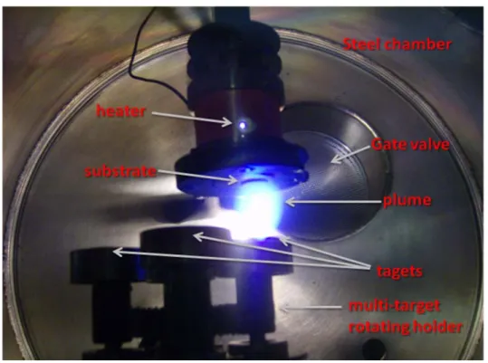
The deposition chambers. The deposition chamber is one of the most important components in a PLD system. The chamber is usually equipped with a multi-target rotating holder, allowing a fast switch of the target during the deposition. Other features include a heater, lenses, windows, gas inlet and ultra-high vacuum equipment to ensure a base pressure of 10-8 mbar. The distance between the substrate and the target is about 25 mm. Figure 2 shows a photo of the chamber used in our laboratory.
Figure 2. Photo of the chamber used in our laboratory. The distance between the substrate and the target is about 25mm.
One of the great advantages of PLD is the ease with which in situ multilayer structures and superlattices can be formed. In fact, a multi-target carousel containing several targets can be used in deposition chamber (see fig.2).
Substrate holders and heaters. Usually, the substrate must be heated to produce good adhesion and epitaxy. For our epitaxial thin films deposited by PLD, substrate temperatures of 600°C must be maintained in ambient oxygen (from 10-3 to 10-1 mbar). On the contrary, porous thin films were deposited at room temperature and annealed after the PLD deposition.
Vacuum equipment. One of the advantages of PLD, as compared to other film deposition techniques, is that a PLD system needs a relatively simple and economical
22
pumping and gas flow systems. Our systems consist of a turbo molecular pump for high vacuum (~ 10-8 mbar) and rotary pump for pre-vacuum (~ 10-3 mbar). Vacuum gauges were used to check the pressure inside the chamber during the deposition.
2.3 X-Ray Diffraction technique for structural
characterization of thin films
The X-ray diffraction technique reveals information about the crystallographic structure of materials and thin films. The basis of diffraction analysis is wave interference: X-ray wavelengths are comparable with inter-atomic distances of the crystal. The interference is constructive when the phase shift is a multiple of 2π, in accordance with Bragg’s law:
θ λ 2dsin
n = (1)
where n is a integer, λ is the wavelength of the incident radiation, d is the spacing between the planes in the atomic lattice and θ is the angle between the incident ray and the scattering planes [2].
Rocking curve. From the rocking curve (RC) it is possible to estimate the film mosaic spread. In the RC procedure, the detector is positioned at the 2θ Bragg position while the angle between the incident ray and the surface of the sample is moved around the Bragg’s angle θ (fig.3).
Figure 3. Rocking curve experimental setup.
From the value of Full Width at High Maximum (FWHM) we can understand how grains are tilted in the film. For this reason a lower value of FWHM means a higher quality of the crystal and lower disorder of the films (fig.4a).
Reciprocal Space Maps. Reciprocal space maps (RSMs), consisting of a series of RC’s, show the distribution of the diffracted X-rays in reciprocal space (RS) in a two dimensional way. Different distortions of a perfect crystal or a heterostructure can be identified by their characteristic shape in RS [2-5]. By RSM we can understand the strain status: the relative positions of the reciprocal lattice points reflect the strain status of the layers and the plane tilts (fig.4b).
24
Figure 4. Representation of the rocking curve (a) and reciprocal space maps (b).
From the angular positions of the layer peaks in the asymmetric map [2-5], the reciprocal lattice vector components qx and qy parallel and perpendicular to the film
surface respectively are:
) 2 2 sin( ) 2 2 sin( 4 θ θ θ λ π − = x q ) 2 2 cos( ) 2 2 sin( 4 θ θ θ λ π − = y q (3)
For the asymmetrical (hkl) reflection the reciprocal lattice vector components depend on the in-plane lattices constant ap and the perpendicular to the film surface
an (for a cubic compound):
p
x h k a
q =2π 2 + 2 /
qy =2π l2 /an (4)
2.4 Electrochemical characterization: Electrochemical
Impedance Spectroscopy (EIS)
Impedance spectroscopy (IS) is powerful method for characterizing many of the electrical properties of materials and their interfaces with electronically conducting electrodes. It may be used to investigate the dynamics of bound or mobile charge in the bulk or interfacial regions of any kind of solid or liquid material: ionic, semiconducting, mixed electronic–ionic, and even insulators (dielectrics). The most common and standard approach to using the EIS technique is to measure impedance by applying a single-frequency voltage or current to the interface and measuring the phase shift and amplitude, or real and imaginary parts, of the resulting current at that frequency using either an analog circuit or fast Fourier transform (FFT) analysis of the response. Commercial instruments (for example the solartron used in our laboratory) are available which measure the impedance as a function of frequency automatically in the frequency ranges of about 1mHz to 10MHz.
26
Any intrinsic property that influences the conductivity of electrodes, electrolytes and in particular solid oxides fuel cell systems can be studied by EIS. The parameters derived from an EIS spectrum fall generally into two categories: (a) those pertinent only to the material itself, such as conductivity, dielectric constant, mobility of charges, equilibrium concentrations of the charged species, and bulk generation– recombination rates; and (b) those pertinent to an electrode–material interface, such as adsorption–reaction rate constants, capacitance of the interface region, and diffusion coefficient of neutral species in the electrode itself [6].
A signal V(t)=Vm⋅sinωt where ω =2πf is applied to a cell and the resulting state current )i(t)=I0⋅sin(ωt+θ measured. θ is the phase difference between the voltage
and the current. The impedance of the electrochemical system is
i V
Z = . Now we
can write the impedance as a complex function of ω :
[ ]
Z(ω) j Im[ ]
Z(ω) ' '' Re ) (j exp ) ( Z ) ( Zr ω = r ω ⋅ φ = r + ⋅ r = Z+jZwhere j= −1. The impedance is a vector quantity and may be plotted in the plane with either rectangular or polar coordinates, as shown in Figure 5.
Figure 5. The impedance Z plotted as a planar vector using rectangular and polar coordinates.
The interpretation of a spectrum of impedance is based on its comparison with a model defined “equivalent circuit”[6].
Properties of equivalent circuits:
• The spectrum of the equivalent circuits must be similar to the system under investigation
• Each element (for example R or C) must be associated with the electrochemical process in the system under investigation.
• The number of elements should be as low as possible The main elements of equivalent circuits are shown in table 1:
Element Symbol Impedance Nyquist plot
Resistance R R Zr= ‐Im(Z) • Re(Z) Capacitance C ωC j Zr =− ‐Im(Z) ω Re(Z) Inductance L L ω j Zr = Re(Z) ω Im(Z)
28 45 45 Phase costan elements CPE
( )
jω -α A Zr = ‐Im(Z) ω α Re(Z) Warburg impedance (relative to the diffusion ) ∞ W ω 1 R Zr = W − j ‐Im(Z) ω 45° Re(Z) Warburg impedance(relative to the diffusion across the thin film with no blocking interfaces ) W D δ jω D δ jω tanh R Z 2 2 W = r ‐Im (Z) ω 45° Re(Z) Warburg impedance (relative to the diffusion across the thin film with
blocking interfaces ) Wb D δ ω j D δ ω j coth R Z 2 2 W = r ‐Im(Z) ω 45° Re(Z)
Table1
2.5 Defects in Oxides
Oxides used for SOFC applications, depend on the types, concentrations and mobilities of the ionic and electronic defects. The defects prevalent in an oxide depend strongly on oxygen partial pressure. In this thesis, we focused on transport mechanisms of doped ceria, because cerium cations are reduced from Ce4+ to Ce3+ at high temperatures and low oxygen partial pressures, resulting in a n-type semiconducting behavior [7]. The electronic contribution to conductivity is known to lead to a drastic decay of SOFC performance and for this reason it is important to know the behavior of the SDC electrolyte at low oxygen partial pressure. Defect concentrations are correlated with Brouwer diagrams (see fig.6). At the stoichiometric composition, the concentration of oxygen vacancies and oxygen
30
interstitials must be equal. At high oxygen partial pressures, excess oxygen can be incorporated through the formation of excess oxygen interstitials. At low oxygen partial pressures, a deficiency in oxygen content can be accommodated through the formation of excess oxygen vacancies [8]. The concentrations of electronic defects are also dependent on oxygen partial pressure from the equations:
2 2 / 1 2 2 / 1 2 ] [ 1 ] [ ] [ ' 2 ) ( 2 1 2 2 V n P V n P O K O e V gas O O O O O O o O • • • • • • = = = + + (5)
At low oxygen partial pressure, the concentrations of electrons (n) and oxygen vacancies are much larger than those of any other defect, so the charge neutrality requires: n VO••]= [ 2 (6) In which case: 6 / 1 3 / 1 2 ) / 2 ( − = K PO n (7)
In intermediate oxygen partial pressures, where the concentration of intrinsic anion Frenkel pairs(VO +Oi '')
•
• is high, the concentration of oxygen vacancies is much
larger than the concentration of electrons, so Equation 7 becomes:
4 / 1 2 / 1 2 2 / 1 2 2 / 1 2 2 2 ]) [ / 2 ( ] [ 1 ] [ ] [ •• − • • • • = ⇒ = = O O O O O O O P V K n n V P n V P O K (8)
Figure 6. Brouwer diagrams.
In general, the exponents in the equations 7 and 8, with slope= -1/4 or slope= -1/6 in the logarithmic scale in the Brouwer diagram, are important for understanding the reduction mechanisms in doped and un-doped oxides [12].
The different regions in the Brouwer diagram are useful for different types of sensors and electrolytes. Oxides for SOFC applications require that the ionic conductivity, represented in the Brouwer diagram by the region where [VO ]=[Oi '']
•
• in the fig 6,
is much higher than the electronic conductivity, and thus would be used in intermediate oxygen partial pressures in the region labeled “solid electrolyte” in figure 6. Often the dopants are added to increase the concentration of ionic defects and extend the range over which the oxide is electrolyte [7-8]. For example in this thesis ceria oxide (CeO2) doped with samarium (SDC) or gadolinium (GDC) and
32
zirconia doped with yttria (YSZ) were characterized at high, intermediate and low oxygen partial pressure. The reactions of these materials are:
From equation 7 and 8, the oxygen partial pressure dependence for conductivity of semiconducting oxide is in the form:
m O KP1/ 2 =
σ
(10)where m can vary from -4 to -6.
2.6 Experimental setup for EIS
In this thesis, the AC impedance spectroscopy measurements were carried out for thin films deposited onto insulating substrates in two point configuration with electrodes deposited onto the film surfaces. We measured the parallel conductivity perpendicular to the growth direction and parallel to the interfaces (figure 7a).
The electrodes deposited onto electrolyte were characterized in sandwich configuration (figure 7b).
Figure 7. typical two-point electrode configuration for AC impedance spectroscopy: a for thin films deposited onto single crystal substrates, b for porous electrodes deposited onto electrolytes.
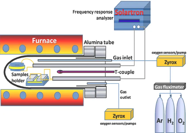
EIS measurements were performed in plane configuration using a frequency response analyzer (FRA, Solartron 1260), coupled with a dielectric interface (Solartron 1296), in the 400–800°C temperature range and in the 0.01 Hz - 10 MHz frequency range, with a 100 mV alternate current signal. Transverse impedance measurements were not carried out because the thin films were deposited onto single crystals substrates. Zview® (shareware version) software was used to fit the EIS data. Electrical conductivity measurements of the films were carried out in the 10-25 - 1 atm pO2 range. Air, pure oxygen, argon, and 5% hydrogen-argon dry mixtures were used to vary pO2. Total gas flow was 150 sccm. Flow rates were controlled by digital flow-meters (MKS). The oxygen concentration was measured using two oxygen sensors/pumps (Zyrox) placed at gas inlet and outlet, respectively. Figure 8 shows a
34
schematic setup for the two point conductivity measurements as a function of the temperature and oxygen partial pressure.
Figure 8. Schematic setup for the two point conductivity measurements as a function of the temperature and oxygen partial pressure.
References
[1] Douglas B. Chrisey, Graham K. Hubler, Pulsed Laser Deposition of Thin Films, John Wiley & Sons, Inc., Publication.
[2] G. Bauer, J. Li, E. Koppensteiner, J. Crystal Growth, 1995, 157, 61. [3] P.F. Fewster, Appl. Phys. A, 1994, 58, 121.
[4] B.K. Tanner, in: Analysis of Microelectronic Materials and Devices, Eds. M. Grasserbauer and H.W. Wemer (Wiley, New York, 1991) 609.
[5] E. Koppensteiner, G. Bauer. H. Kibbel and E. Kasper, J.
Appl. Phys., 1994, 76, 3489.
[6] Evgenij Barsoukov, J. Ross Macdonald, Impedance Spectroscopy Theory, Experiment, and Applications, John Wiley & Sons, Inc., Publication.
[7] M. Mogensen, N.M. Sammes, G.A. Tompsett, Solid State Ionics 2000, 129, 63.
Chapter 3
Structural and electrochemical
characterization of epitaxial
Samarium-doped ceria thin film
3.1 Introduction
The growing demand for miniaturized systems for energy conversion and storage has prompted extensive research aimed at the fabrication of solid state ionic devices in thin film form. Electrochemical devices, such as solid oxide fuel cells (SOFCs), can be miniaturized for portable applications (µ-SOFCs) [1]. This goal requires the reduction of the operating temperature and the production of components as thin films [2-7]. In general, µ-SOFC devices are expected to produce energy densities per volume and specific energy per weight up to four times larger than state-of-the-art rechargeable Li-ion and Ni metal hydride batteries [8].
Samarium and gadolinium doped ceria (SDC, GDC) possess larger ionic conductivity than yttria-stabilized zirconia (YSZ), the conventional SOFC electrolyte material, and are thus intensively studied to achieve the target of reducing SOFC operating temperature in the 600-800 °C range [9-11].
However, doped ceria is a mixed ionic-electronic conductor (MIEC), because cerium cations are reduced from Ce4+ to Ce3+ at high temperatures and low oxygen partial pressures, resulting in a n-type semiconducting behaviour related to the small polaron hopping mechanism [12]. The electronic contribution to conductivity is known to lead to a drastic decay of SOFC performance; however, such contribution is negligible at low temperatures for doped ceria, allowing its use as IT-SOFC electrolyte. Doped-ceria is particularly promising as electrolyte for µ-SOFCs, as demonstrated by the numerous papers recently appeared in the relevant literature investigating doped ceria in thin film form [5, 7, 13-19]. Pulsed laser deposition (PLD) is particularly promising amongst the different film deposition techniques, because of its capability of reproducing the target composition onto the film substrates [20].
3.2 Epitaxial thin films and heterostructures deposited onto
single crystal perovskite substrates
Doped ceria films having fluorite structure can be deposited, starting from a polycrystalline target, on several non-fluorite substrates maintaining the correct stoichiometry [19]. In particular, doped ceria has been shown to grow on (001) MgO substrates as well as on (001) LaAlO3 (LAO), (110) NdGaO3 (NGO), and (001)
38
SrTiO3 (STO) perovskite substrates [14,16]. Perovskite-type substrates provide the proper lattice match for ceria, inducing the growth of epitaxial monocrystalline films with a low degree of structural disorder [16]. The growth condition for SDC on NGO were: oxygen partial pressure in the deposition chamber about 4 x 10⁻³ mbar, the temperature of substrate about 630°C. The laser fluence was set at approximately 5 J/cm2 with repetition rate of 10 Hz. The distance target substrate was about 2.5 mm. Figure 1 shows the XRD plots (θ-2θ fig.a and rocking curve fig. b) of Samarium oxide (20 mol%)-doped ceria (SDC) thin film deposited onto NGO single crystal. In the θ-2θ scan of Fig. 1a, only the (002) diffraction peaks from the NGO substrate and the SDC film were detected. This indicated a [001] preferential orientation for the SDC film growth. The rocking curve of the (002) SDC film peak in figure 4b showed a FWHM value of about 0.1°. Small FWHM values demonstrate a very low degree of crystallographic disorder for the deposited film.
20 25 30 35 40 45 50 a. SDC/NGO (001) i n te n s it y (ar b . u n it s ) NGO (002) NGO (002) SDC 002 2 θ (degrees) 14 15 16 17 18 19 b. FWHM=0.11° in tensit y (arb. u nit s) θ(degrees) rocking curve SDC (002)
Figure 1. θ-2θ scan (a) and rocking curve (b) of SDC deposited onto NGO perovskite.
Figure 2 shows the XRD plots of tri-layer of LSCF/SDC/LSCF deposited onto STO single crystal substrates deposited at 600°C and 10-4mbar oxygen partial pressure. XRD plots demonstrate a very low mosaic spread for the tri-layers LSCF/GDC/LSCF and LSCF/GDC/ESB/GDC/LSCF.
25 30 35 40 45 50
intensity (arb. units) STO(001)
STO(002)
LSCF(022) GDC(002)
LSCF/GDG/LSCF-STO
2
θ
(degrees
)Figure 2. θ-2θ scan of heterostructures of LSFC/SDC/LSCF deposited onto STO
Figure 3 shows a XRD scan of heterostructures of LSCF/SDC/ESB/SDC/LSCF deposited onto STO substrate at the same growing condition of SDC and LSCF/GDC/LSCF deposited onto STO.
40 20 25 30 35 40 45 50 STO (002) STO (002) LSCF (002) ESB (002) GDC (002) in te n s ity (a rb.units. )
2
θ
(degrees
) LSCF-GDC-ESB-GDC_on STO (001)Figure 3. θ-2θ scan of heterostructures of LSFC/GDC/LSCF deposited onto STO. XRD plots (fig.5 and fig.6) demonstrate a very low mosaic spread for the tri-layers LSCF/GDC/LSCF and LSCF/GDC/ESB/GDC/LSCF.
Figure 4 shows a FE-SEM micrograph of the cross section of tri-layer of LSCF/SDC/LSCF deposited onto STO single crystal substrates after deposition without annealing treatment.
Figure 5 shows the top-view of the tri-layers LSCF/GDC/LSCF annealed at 800°C for 12 hours. The morphology confirms a very low mosaic spread for the tri-layers LSCF/GDC/LSCF. Bottom LSCF (fig. 5d and 5c) and GDC (fig. 5c, 5b and 5a) are dense, homogeneous, and continuous and grain boundary regions are not revealed. On the contrary top LSCF layer (fig. 5a) is not dense but it is formed by crystals with size of about 100 nm.
Figure 5. FE-SEM of the surface of LSFC/GDC/LSCF deposited onto STO.
However, perovskite substrates might show electronic, ionic, or mixed ionic-electronic conduction at temperatures above 300 °C, which might affect the proper
42
evaluation of the electrical measurements performed on ceria films. Namely the electrochemical measurements of SDC/YSZ bi-layer deposited onto STO single crystal (fig.6), with the overall thickness of about 400 nm, shows typical behavior of p-type conductor of perovskite in air and at low pO2. Figure 6 shows a Brouwer diagram of bi-layer of SDC/YSZ deposited onto STO single crystal. From the total electrical conductivity as a function of oxygen partial pressure in the fig.6 is clearly evident the absence of the contribution of the thin film in the electrochemical measurements. Namely the conductivity, calculated with geometrical factor of the film (overall thickness about 400 nm, about 2 mm distance between the electrodes and 5mm the electrode width normal to the current flow) in the Brouwer diagram exhibits the tipical behaviour of the substrate STO [21, 22].
-24 -20 -16 -12 -8 -4 0 4 -1.6 -1.2 -0.8 -0.4 0.0 0.4 0.8 1.2 1.6 2.0 600 °C 700 °C 500 °C 700 °C Log( σ ), S c m -1 Log(pO 2), atm 600 °C
YSZ/SDC STO substrate
Figure 6. Total electrical conductivity of B-layer SDC/YSZ deposited onto STO substrate as a fuction of oxygen partial pressure.
3.3 XRD characterization of SDC and SDC/STO deposited
onto MgO (001) single crystal substrate
MgO, which shows a remarkably low electrical conductivity at high temperatures, does not provide a good lattice match with the ceria fluorite structure, namely the lattice misfit between SDC and MgO is about 8.63%. As a consequence, doped ceria films on MgO show a higher degree of structural disorder, which can result in ionic conduction blocking effects and to contaminant segregation phenomena [13, 23].To obtain a proper evaluation of the conductivity of epitaxial or single-crystal doped-ceria films, in this work PLD was used to grow highly doped SDC (20% molar samarium oxide) films on (001) MgO single-crystal substrates, using a STO thin film as a buffer layer, taking advantage of the good lattice match between MgO and STO that allows the epitaxial growth of STO films on MgO substrates. A similar approach has been previously used for the deposition of high temperature superconductor thin films onto MgO substrates [24-26]. The SDC/STO/MgO heterostructure was engineered in order to combine the chemical and thermal stability of the insulating MgO substrates with the structural properties of the SDC films grown on the perovskite structures. The STO buffer layer matched well both SDC and MgO. The STO thickness was kept at about 50 nm, introducing a negligible electronic contribution to the overall conductivity of the heterostructure. This allowed for the first time, to the best of our knowledge, the measurement of the ionic conductivity of epitaxially-ordered Sm-doped ceria thin films decoupling any interference from the substrate electronic conductivity.
44
X-ray diffraction (XRD) analysis showed that the materials used as targets and substrates in the PLD were single phase. The lattice parameters for starting materials, deposited films, and MgO substrates were calculated from XRD analysis, showing a good agreement between the experimental values and those reported in the literature [27-29]. Figure 8 shows the θ-2θ XRD patterns of the SDC/MgO film.
30
35
40
45
SDC/MgO (002)
MgO
(002)
Intensity (
a
rb. units)
SDC
(002)
2
θ (
degrees)
Figure 6. θ-2θ XRD plot of the SDC/MgO.
Figure 7 shows the rocking curves of the (002) diffraction peak for the SDC film deposited on MgO.
10 15 20 25
Intens
ity (arb. units)
(002) SDC
FWHM=3.5°
θ
(degrees)
Figure 7. rocking curve of the (002) diffraction peak for SDC/MgO.
In the θ-2θ scan of Fig. 1, only the (002) diffraction peaks from the MgO substrate.
This indicated a [001] preferential orientation for the SDC film growth. The rocking curve of the SDC (002) reflection showed a full width at half maximum (FWHM) value of about 3.5°. Such a large FWHM value demonstrated a rather elevated degree of crystallographic disorder for the SDC film. This result is a consequence of the large lattice misfit of 8.63 % between MgO (a = 4.21 Å) and the SDC20 (a = 5.44 Å) structures. Fig. 8 shows the θ-2θ scan for the SDC/STO/MgO heterostructure: only the (002) diffraction peaks from the MgO substrate, STO buffer layer, and SDC film are visible.
46 30 32 34 36 38 40 42 44 46 SDC/STO/MgO (001) MgO (002) In te ns it y ( a rb . un it s) STO (002) SDC (002)
2
θ
(degrees
)Figure 8. θ-2θ scan for the SDC/STO/MgO heterostructures.
This indicates that both buffer layer and film grew with the [001] axis perpendicular to the substrate surface. Moreover, the rocking curve of the (002) SDC film peak in figure 4 showed a FWHM value of about 0.3°. Small FWHM values demonstrate a very low degree of crystallographic disorder for the deposited film.
12 14 16 18 20 Intensity (arb.units) FWHM=0.3° θ (
degrees
) SDC (002)rocking curve SDC/STO/MgO (001)
Such a result confirmed that the STO (a = 3.91 Å) buffer layer is able to withstand the large lattice mismatch between MgO and SDC with a relatively low number of misfit dislocations at the interface. The epitaxiality relationship among the different layers in the SDC/STO/MgO heterostructure was investigated by the φ-scan technique. Figure 10 shows the φ−scan XRD of SDC grown on a (001) MgO substrate with a buffer layer of STO.
60 120 180 240 300 360 MgO (113) In ten s it y (ar b . uni ts ) SDC(113) & STO (103)
φ (
degrees)
Figure 10. φ−scan XRD of SDC grown on a (001) MgO substrate with a buffer layer of STO.
The φ-scan of the SDC/STO/MgO heterostructure over 360° was first recorded keeping both the Bragg angle and the incidence angle set at the (113) MgO asymmetric reflection: four peaks having approximately the same intensity and a relative distance of 90° were detected. The same measurement was repeated for the STO and SDC layers. In the case of the STO buffer layer, the (103) asymmetric reflection was used instead of the (113) reflection because of its larger intensity. φ-scan of the (103) asymmetric reflection of the thin STO buffer layer showed four
48
peaks with 45° degree displacements with respect to the (113) MgO peaks (dashed lines in Fig. 10), proving the in plane “cube on cube” match between the two materials. Finally, a φ-scan of the (113) SDC reflection was taken, which showed the occurrence of four peaks at the same φ-angle values as the STO (103) diffraction peaks. This indicates that the SDC fluorite film grew with a 45° in-plane rotation of the cubic crystallographic axes relative to the orientation of both STO and MgO. Figure. 13 shows a sketch of the epitaxial relationship between the SDC fluorite structure and the STO perovskite structure, as derived from the data of figure 11.
Figure 11. Schematic sketch of the correlation between the cubic cells of SDC, STO and MgO.
The 45° rotation of the SDC fluorite structure with respect to STO can be explained on the basis of simple structural considerations. SDC (fluorite structure) and STO (perovskite structure) have cubic lattice parameters of about 5.44 Å and 3.91 Å, respectively. Therefore, the STO basal diagonal, calculated to be about 5.53 Å, matches quite well the lattice parameter of the SDC fluorite (5.44 Å), with a misfit
percentage value of 1.62 %. Such a value is low if compared with 8.63 % present at the SDC/MgO interface and also to 7.12 % at the STO/MgO interface. XRD measurements taken after a post annealing treatment and measurements showed that the deposited films preserved the crystalline quality observed in figures. 8, 9 and 10. Lattice misfits at the films interfaces between the deposited film and the substrate is a crucial factor for the residual stress formation in the films structure and it is the main cause for a mosaic-spread epitaxial film growth and for their mechanical failure in operative condition [7, 19]. As shown by the XRD analysis, SDC/MgO presented high misfit value which can lead to stress conditions in the SDC film. On the other hand, STO-buffered SDC presented low lattice misfits and low residual stress are expected. The table 1 shows the misfit between SDC and substrates.
Misfit %
MgO
STO
SDC
8.63
1.62
Table 1
3.4 Morphological characterization of SDC and
SDC/STO/MgO (001)
Figure 12 shows the FE-SEM micrographs of the cross-sections (fracture surface) and surface-views (in inset) of the SDC/MgO structure post-annealed at 800 °C for 1 hour in air.
50
Figure 12. FE-SEM micrograph of cross-section and surface (in inset) of SDC/MgO (001).
Figure 13 shows SDC/MgO (001) tested for several days in reducing-oxidizing conditions in the 400-775 °C range. Figure 13a. shows the cross-section SDC/MgO (001) and figure 8b shows the surfaces of the sample.
Figure 13. FE-SEM micrograph of the cross-section (a) and surface of the SDC/MgO tested for several days in reducing-oxidizing conditions in the 400-775 °C range.
Fig. 13 shows that the annealed SDC film was dense and homogeneous on the MgO substrate with a columnar morphology. The plan view images (fig. 13) showed a
52
highly textured columnar structure with a mosaic-spread arrangement in the nanometric scale. Such morphology showed instability during the thermal treatments in hydrogen and oxygen atmospheres. Figure 13a shows that SDC film lost adhesion from the MgO substrate, probably due to stress induced by the lattice misfit between SDC and MgO. However, fig. 13b shows that the columnar grains, in the treated film, changed their morphology from the textured structure (fig. 13) to a cylindrical shape. This evolution occurred with time at temperatures below 800 °C, upon a few oxidation-reaction cycles, and led to the formation of micro-cracks and nanometric porosity (fig. 13b). The microstructural evolution of SDC/MgO samples was explained by the fact that the annealed film (fig.13) presented a high surface energy at the grain boundary and at the SDC/MgO interface. This energy could be released in the diffusive regimes that can be activated also at low temperatures [11]. Despite several papers in the relevant literature reported electrical results obtained for columnar polycrystalline thin films of doped ceria, their long term thermal and chemical stability has been scarcely considered [7]. However, thermal stresses and microstructural evolution for thin films is crucial for µ-SOFC applications, usually subjected to reduction and oxidation cycles at elevated temperatures. Our results clearly showed a marked instability at high temperatures of ceria thin films deposited by PLD after a few red-ox cycles, demonstrating that problems might arise from the fuel cell operation of these films.
Figure 14 shows the FE-SEM micrograph of the cross-section (fracture surface) of the SDC/STO/MgO heterostructure post annealed at 800 °C for 1 hour and measured in the 400-775 °C range in reducing-oxidizing conditions for several weeks. The
SDC and STO films were dense, homogeneous, and continuous, with no delamination at the materials interfaces. The samples were stable even after several red-ox cycles used for the electrical measurements.
Figure 14. FE-SEM micrograph of the cross-section (fracture surface) of a film of SDC grown on a (001) MgO substrate with an STO buffer layer, post annealed at 800 °C for 1 hour.
Observation of the sample surface morphology and the cross-section did not show the presence of grain boundaries. The thickness of the SDC and STO layers was about 260 and 50 nm, respectively. It is expected that the contribution of the STO buffer layer to the electrical conductivity of the SDC/STO/MgO heterostructure would be negligible because of the relative thicknesses of the SDC and STO layers, estimated by FE-SEM observations. In fact, the electrical conductivity was measured in-plane, by depositing on the SDC film two Au electrodes having a 4 x 5 mm area,
54
a significant contribution to the electrical measurements is the fact that the conductivity of the SDC/STO/MgO and SDC/MgO have the same value before the degradation of SDC/MgO. However, contributions from the STO-SDC interface and from the STO buffer layer must be considered to occur when evaluating the electrical measurements performed in conditions of dominant electronic conduction mechanisms for SDC [30].
3.5 Electrochemical characterization of SDC/MgO (001)
and SDC/STO/MgO (001)
Electrochemical impedance spectroscopy (EIS) analysis allows the separation of the electrolyte impedance contribution (at high frequencies) from the electrode impedance contributions (at low frequencies). EIS measurements can be performed using a two electrode configuration, allowing avoiding the use of a reference electrode that is difficult to place in a thin film-shaped sample [31].
Figure 15 shows typical Nyquist (fig.15) and imaginary part of the complex impedance, –Im(Z), measured in air at 700°C, for the post-annealed SDC/STO/MgO and SDC/MgO films.
0 20 40 60 80 100 120 140 160 180 200 0 20 40 60 80 100 104Hz 105Hz SDC/MgO 106Hz 103Hz 104 Hz 700 °C, Air -I m( Z) , k Ω Re(Z), kΩ SDC/STO/MgO 105Hz
Figure 15. Nyquist (a) and –Im(Z) vs frequency plots (b), measured in air at 700°C, for the post-annealed SDC/STO/MgO and SDC/MgO films.
As is well known [32-33] a semicircle on the complex impedance plot is due to a resistive (R) and a capacitive (C) element in parallel. For both samples, the Nyquist plots exhibited a single semicircle, with a very similar R value of about 150 kΩ. The SDC/STO/MgO sample did not exhibit grain boundaries and the single semicircle at high frequencies can be ascribed to bulk ionic conductivity.
Usually for polycrystalline ionic conductors, the Nyquist plots typically show two separated semicircles (series of two RC elements in parallel), which are attributed to conduction mechanisms at bulk (high frequency semicircle) and at the grain boundary (low frequency semicircle) [12]. In some circumstances, those two semicircles might be overlapped depending on the respective R and C values, making difficult the separation between bulk and grain boundary contributions. However, plotting the EIS data with different formalisms might allow the separation of the two peaks, if present [35]. An evaluation of the EIS data in figure 15 with other
56
formalisms did not show the presence of other peaks, confirming the presence of a single RC element for both the samples. The capacitance value measured for the SDC/MgO sample is on the upper range of values typical for doped-ceria grain boundary conductivity [33]. A single semicircle was measured also for the polycrystalline SDC/MgO samples. Therefore, considering the film morphology, in this case the RC element was attributed to the grain boundary contribution, due to the fact that the nanometric size of the crystals minimizes bulk conduction contribution [3]. Moreover, the in-plane cell configuration used for EIS measurements should expand grain boundary contribution since the current lines pass across the columnar grain boundaries. Therefore, the samples can present predominant bulk or grain boundary contributions depending on their microstructural features, as expected from SEM observations. The Nyquist plots at low frequencies (f < 1 kHz) for both the samples showed limited polarization and scattering phenomena at the Au electrodes. This fact was probably due to the high temperature used for the measurements and the low impedance values associated with polarization phenomena. Polarization at lower temperatures could not be evaluated because of the high impedance values of the samples at low temperatures reached the instrument resolution limits. Figure. 16 shows the Arrhenius plots in the 400 - 775 °C temperature range measured for the post-annealed SDC/MgO (fig.16a) and SDC/STO/MgO (fig. 16b) films in air and in Ar-H2 mixtures at different pO2. The total conductivity σtot was evaluated by the Ri
values obtained by the single semicircle registered by the EIS measurements at all the temperatures. Figure 16 a shows the conductivity for SDC/MgO samples
measured in air in two different cooling ramps from 775 to 400 °C (in fig. 16 a, I and II cycle) and at 600 °C at pO2= 10-3 atm and pO2 =10-25 atm (see zoom in the inset).
-4 -3 -2 -1 0 1 1,10 1,15 1,20 -3 -2 -1
1,0
1,2
1,4
1,6
1,8
-4 -3 -2 -1 0 1 E a=0.47(1) e Vb.
Air: I cycle Air: II cycle pO2 = 10-25 atm pO2 = 10-22 atmLog(
σ
), S
c
m
-1
SDC/MgO
E a=0.7 75(13) e V 600 °Ca.
8days E a=0.7 4(6) eV E a=0.9 4(1 ) eV E a=0.9 5(3 ) eVSDC/STO/MgO
air pO2= 10-22 atm pO2=10-25 atm 1000/T, K-1Log(
σ
), Scm
-1
Figure 16. Arrhenius plots in the 400 - 775 °C temperature range measured for the post-annealed SDC/MgO (a) and SDC/STO/MgO (b) films in air and in Ar-H2 mixtures at different pO2.
58
Measurements were collected in about 14 days: each cycle was carried out in 3 days, and the measurements at low oxygen partial pressures required 8 days to reach the balance with the atmospheres. From these data typical activation energy, for temperatures above 600 °C, was calculated to be about 0.775 eV and below 600 °C to be about 0.47 eV. Such values are lower than the values 0.8-0.9 eV usually reported for polycrystalline doped-ceria grown thin films[37]. Particularly, at lower temperatures the Ea resulted close to the activation energy values reported for electron hopping mechanism phenomena for ceria and doped ceria [37]. However, the conductivity data collected revealed the instability of the SDC/MgO sample. Particularly, the conductivity decreased in air of 30-40 % from the I cycle to the II cycle. However, conductivity decreased drastically of around 2 magnitude orders in 8 days, when the sample was exposed to hydrogen atmospheres (inset fig. 18a). Such degradation was irreversible since the conductivity did not return to the values registered when, finally, the sample was re-exposed to air. An explanation to such a conductivity decay was found to be the microstructural instability which led to the cracks and porosity formation observed in the SDC/MgO sample (fig. 13). On the other hand, the SDC/STO/MgO sample was observed to be stable for all the time of measurements and the data were repeatable for all the temperatures and atmospheres. In this case Arrhenius plots could be drawn in air and in low oxygen partial pressure atmospheres. Figure 16b shows that sample conductivity increased with decreasing pO2. σtot in air at 700 °C was evaluated to be about 7 10-2 S cm-1. Such a value is
larger than conductivity value (~2 10-2 S cm-1 at 700 °C) measured for the dense polycrystalline pellets obtained by a conventional sintering of the SDC powders [11].
Both stability and enhanced conductivity of SDC films onto STO buffer layers was attributed to the low disorder of the epitaxial deposition, resulting in the absence of grain boundaries, which means absence of conduction blocking effects and of high energy unstable regions. The calculated activation energies, Ea, for the
SDC/STO/MgO film were found to be 0.74 eV in air, 0.94 eV for pO2 = 10-22 atm, and 0.95 eV for and pO2 = 10-25 atm. This can be explained in terms of different conduction mechanisms in air and at low pO2. Ea values in air correspond to the
typical activation energies reported for ionic conduction in doped-ceria bulk and thin film shapes [14, 18]. The conductivity enhancement at low pO2 can be attributed to electronic conductivity related to the Ce reduction at low pO2 [13, 14, 18, 35]. The typical process of ceria reduction may be written as:
) 2 ( 2 ) ( 2 1 2 ' ' 2 gas V Ce e O Ce Oo + Ce = + O•• + Ce (2)
where the Kröger-Vink notation has been used, and [ ••]
O
V represents the oxygen
vacancy concentration in doped ceria. The associated equilibrium constantKris:
2 / 1 2 ] [V n pO Kr = •• (3) where [ '] e
n= represents the electron concentration. In mixed ionic-electronic
conductorss, the total electric conductivity, σtot, is given by two contributions: ionic,
ion
σ , and electronic, σe. The relation between σeand oxygen partial pressure pO2 is
described by the Brouwer equilibrium equation:
r r e K pO − = ( 2) σ (4)
where r is usually 1/4 or 1/6 for doped ceria, depending on the stoichiometry of the electrochemical reduction reaction [12]. On the contrary, σion does not depend on
60
pO2 because the VO••concentration is nearly independent from the cerium valence state [12].
Therefore, to evaluate the Brouwer equilibrium equation and the electronic conductivity of the ceria films, EIS measurements were performed in a wide range of oxygen partial pressures. Figure 17 shows the Brouwer diagram for the SDC/STO/MgO sample obtained from EIS measurements at 400 °C, 500 °C, 600 °C, and 700 °C. σtot was constant in a pO2 range whose width depended on the
temperature.
-25
-20
-15
-10
-5
0
5
-3.0 -2.5 -2.0 -1.5 -1.0 -0.5 0.0 700 °C 600 °C 500 °C 400 °CLog(
σ
), Scm
-1
Log(pO
2), atm
SDC/STO/MgO
-1/6 -1/4Figure 17. Total electrical conductivity as a function of oxygen partial pressure for the SDC/STO/MgO sample at 400, 500, 600, and 700 °C, obtained from EIS
measurements.
In particular, figure 17 shows that at 400°C a plateau (horizontal lines in fig. 17) was observed in the 10-17 atm -1 atm pO2 range. At higher temperatures, the plateau lower

![Figure 3. The resistance of YSZ thin films deposited on MgO substrate as a function of the thickness [3-4]](https://thumb-eu.123doks.com/thumbv2/123dokorg/7605482.114799/15.892.165.632.185.649/figure-resistance-ysz-films-deposited-substrate-function-thickness.webp)

![Figure 7. TEM- micrograph of GDC/ZrO 2 heterostructure deposited onto Al 2 O 3 [6].](https://thumb-eu.123doks.com/thumbv2/123dokorg/7605482.114799/18.892.288.630.560.898/figure-tem-micrograph-gdc-zro-heterostructure-deposited-al.webp)
![Figure 8. Conductivities of single crystal YSZ, and several number of layers at 650K [6]](https://thumb-eu.123doks.com/thumbv2/123dokorg/7605482.114799/19.892.260.611.428.705/figure-conductivities-single-crystal-ysz-number-layers-k.webp)

![Figure 17. The Arrhenius plot of the STO substrate and the heterostructures STO/YSZ/STO [16]](https://thumb-eu.123doks.com/thumbv2/123dokorg/7605482.114799/24.892.258.646.601.987/figure-arrhenius-plot-sto-substrate-heterostructures-sto-ysz.webp)