Pressure-induced metallization process
in Strongly Correlated Electron Systems.
Relatore interno
prof. Giovanni Stefani
Coordinatore
prof. Guido Altarelli
Relatore esterno
prof. Paolo Postorino
Dr. Carlo Marini
A. A. 2009-2010
1.5 Peierls Instability . . . 13
1.5.1 Instability of the electron gas in presence of electron phonon coupling . . . 15
2 Insulator to metal transition 20 2.1 Properties of Solid Tellurium . . . 20
2.1.1 Insulator to metal transition in solid Te . . . 21
2.1.2 Crystal structures of solid Te and phase diagrams . . . 22
2.1.3 Electronic structure of solid Te . . . 25
2.1.4 Other measurements . . . 27
2.2 Properties of Nichel Selenium pyrites . . . 28
2.2.1 Metal-insulator transition in NiS2−xSex . . . 28
2.2.2 Structural properties of NiS2−xSex . . . 30
2.2.3 Electronic structure . . . 31
2.2.4 Other measurements . . . 34
2.2.5 High pressure studies . . . 35
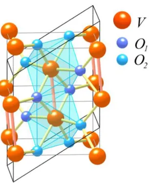
2.2.6 Quantitative Interpretation of Experimental Findings . 38 2.3 Properties of vanadium dioxide . . . 39
2.3.1 Insulator to metal transition in VO2 . . . 41
2.3.2 Structural transition in VO2 . . . 42
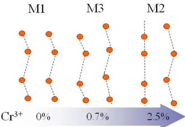
2.3.3 Cr-doped compounds: M2 and M3 phases . . . 44
2.3.5 Role of electronic correlation . . . 48
2.3.6 High pressure studies on pure and Cr-doped VO2 . . . 51
2.4 Measurements plan . . . 54
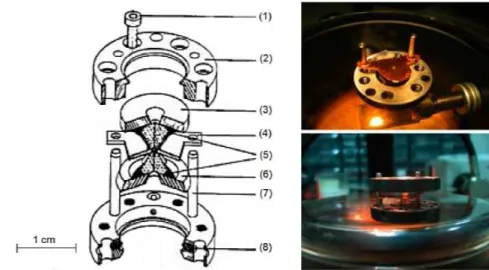
3 Experimental techniques 55 3.1 High pressure technique . . . 55
3.1.1 The high pressure diamond anvil cell . . . 55
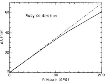
3.1.2 In situ pressure measurement . . . 60
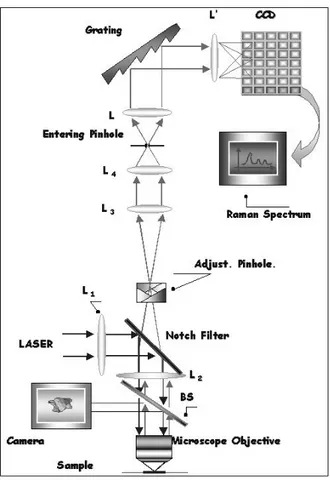
3.2 Raman scattering setup . . . 61
3.3 Infrared setup . . . 64
4 High pressure measurements on solid Te 68 4.1 Optical studies on solid Te . . . 69
4.1.1 Survey of Raman measurements on solid Te . . . 69
4.1.2 Survey of Infrared measurements on solid Te . . . 70
4.2 Synthesis and characterization on solid Te . . . 73
4.3 Solid Te at high pressure . . . 74
4.3.1 High pressure Raman measurements on Te . . . 74
4.3.2 High pressure infrared measurements on Te . . . 78
4.3.3 High pressure DFT calculations on trigonal Te . . . 79
5 High pressure measurements on NiS2−xSex 82 5.1 Optical studies on Ni-pyrites . . . 82
5.1.1 Survey of Raman measurements on NiS2−xSex . . . 82
5.1.2 Survey of Infrared measurements on NiS2−xSex . . . 85
5.2 Synthesis and characterization of NiS2−xSex samples . . . 87
5.2.1 Optical characterization . . . 88
5.3 NiS2 at ambient pressure . . . 89
5.3.1 Infrared vs Se alloying . . . 89
5.3.2 Raman vs Se alloying . . . 90
5.4 NiS2 at high pressure . . . 95
5.4.1 High pressure Raman measurements on NiS2 . . . 95
5.4.2 High pressure Infrared measurements on NiS2 . . . 98
5.4.3 High pressure theoretical calculations on NiS2−xSex . . 100
6 High pressure measurements on VO2 103 6.1 Optical studies on VO2 . . . 103
6.1.1 Survey of optical measurements on VO2 . . . 103
6.2 Synthesis and characterization of VO2 samples . . . 109
6.3 VO2 at high pressure . . . 113
mond anvil cell 141 B.1 Effective reflectivity . . . 142 B.2 Effective transmittance . . . 144 B.3 Optical conductivity from experimental data . . . 146 C Measuring the reference in a Reflectivity measurement: the
evaporation technique 147
Bibliography 149
Understanding the physics of strongly correlated systems is one of the most challenging tasks of condensed matter research. Transition metal and tran-sition metal compounds typically show a large variety of phases different for transport, structural, and magnetic properties on varying internal (e.g. chemical composition, doping ...) and external ( e.g. temperature, pressure, electric or magnetic field, ...) parameters. Such a rich phenomenology is the result of a complex and often delicate balance among several different microscopic interactions simultaneously at work in these systems. Very often indeed it is only through a combined theoretical-experimental investigation of the the effects of magnetic interactions, electron and electron-phonon correlation that a real knowledge of the system can be achieved. These systems thus represent an intriguing scientific problem but their in-trinsic sensitivity to small changes of internal/external parameters and the resulting good possibility of a focused material engineering make this class of systems highly appealing for a wide range of technological applications. The study of the microscopic mechanisms driving the system towards the different regions of the phase diagram and the close analysis of the physics underlaying the phase boundary crossover is the main route to develop reli-able models to reproduce or possibly to predict the physical behavior of these strongly electron correlated systems.
Among all the possible phase transitions, the metal insulator transition (MIT) in these systems is a particularly interesting phenomenon to which the lattice, the electronic, and the spin degrees of freedom of the system often contribute in conjuction. The extent of charge localization/delocalization can be directly affected by charge-lattice coupling triggered by local lat-tice distortions activated via spontaneous symmetry breaking (e.g. Peierls and Jahn-Teller effect) or structural transition which profoundly modify the band structure. On the other side the MIT can originate from pure elec-tronic mechanisms such as electron-electron correlation (e.g. Mott-Hubbard transition) or charge tranfer phenomena. The physical scenario underlying the MIT can be made further complicated when more then one of the above
pression indeed has the effect of increasing the orbital overlap and allows, in principle, to disentangle pure electronic effects from those lattice-mediated. Finally, as observed in the case of some manganite families, reducing the volume can have the effect of enhancing hidden magnetic interactions too weak to be detected at ambient pressure condition.
The present work focuses on three systems where different mechanisms are expected to give rise pressure-induced MITs: the Peierls distorted solid Tellurium, the Mott-Hubbard pyrite NiS2−xSex, and the V1−xCrxO2 where
both Peierls lattice distortion and electron correlation are expected to con-tribute to the spectacular temperure driven MIT (five order of magnitude jump in the conductivity). All the systems have been investigated by means of Raman and Infrared spectroscopy fully exploiting the simplicity and the versatility of diamond anvil cells (DAC) to pressurize the samples. As to the the Infrared measurements we take full advantage of the state-of-the-art performances of the Infrared beamline SISSI at the Synchrotron Elettra (Tri-este). The very small sample dimensions in the DAC (typically 100x100x10
µm) require indeed a source with the very high brilliance of a synchrotron
infrared source. An about equal effort has been devoted in investigating the three systems.
We have at first investigated the MIT in Peierls distorted systems. Rep-resentative of this class of systems is solid Te, an elemental system which shows a complex sequence of high pressure structural and electronic phases, which, as well as for the other elements of the VI group, are still object of debate. At ambient conditions, solid Te has a trigonal structure with helical chains running parallel to the c axes. The unit cell contains three atoms, each having two nearest neighbors within chain with covalent-like bonds, and four second neighbors on the adjacent chains linked by means of Van der Waals interaction. This chain framework may be considered as arising from a Peierls distortion of the six-coordinated simple cubic structure. On increasing the pressure a reduction of the inter-chains distances occurs
lead-ing to a structure symmetrization, accompanied by a charge delocalization process which sets in at 4 GPa.
High pressure Raman and Infrared measurements (0-15 GPa) have been carried out to probe lattice and electron dynamics properties of solid Te around the MIT and in the high pressure metallic phase. From the analy-sis of the pressure dependence of the Raman-active phonon modes we have found evidences of the structural transition at ∼ 4 GPa and, on further in-creasing the pressure, the existence of an incommensurate phase at ∼ 8 GPa recently proposed in the literature. Moreover a careful study of the pressure dependence of the measured phonon peak intensities allowed us to suggest the possibility that an inter-chain charge transfer process may be responsible of the MIT through the removal of the chain distortion. Ab initio Density Functional Theory (DFT) calculation, carried out on trigonal Te and in full agreement with the experimental observations, confirm the above hypothe-sis of pressure induced inter-chain charge transfer by the observation of a sensible reduction of the electron density among the nearest neighbouring Te atoms in-chain in favor of an increase of the electron density toward the second neighbouring Te atom in the adjacent chain. Finally high pressure Infrared measurements, quite recently carried out, give direct evidence of a pronounced dichroism of the system showing different values of the band edge, depending on the polarisation of the incident beam. In this case, on applying pressure, the MIT has been directly observed through the pres-sure induced band gap clopres-sure. It is worth to notice that on approaching the transition at 4 GPa a progressive reduction of band edge anisotropy has been observed in agreement with the idea of pressure induced symmetrization.
The second system investigated has been the Nickel pyrite. Cubic pyrite NiS2is a charge transfer insulator and has attracted interest as it easily forms
a solid solution with NiSe2(NiS2−xSex), which, while being iso-electronic and iso-structural to NiS2, is nevertheless a good metal. The NiS2−xSex pyrite is considered together with vanadium sesquioxide V2O3, a text-book example of
strong correlated electron systems. Since the Se2− p orbitals have larger
spa-tial extension with respect to the S2− ones, the substitution of S with Se in
NiS2−xSex drives the system at room temperature to a bandwidth-controlled
MIT for x ≈ 0.6. An alternative way to induce a metallic state in NiS2 is
applying a hydrostatic pressure. Following Mott’s original idea, this tech-nically challenging procedure offers the unique opportunity to continuously tune the bandwidth, without introducing impurities or disorder.
We have carried out both Infrared and Raman measurements as a function
of x (0-1.2) and pressure (0-12 GPa) on several samples of the NiS2−xSex
pyrite family. Bearing in mind that the lattice volume is expanded by Se-substitution and compressed by pressure an extended volume dependence
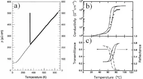
interest in the last decades. On decreasing the temperature, VO2 shows a
MIT accompanied by a simultaneous rutile (R) to monoclinic (M1) structural transition thus masking the real electronic or structural nature of the MIT. The low temperature M1 phase is a distorted R structure characterized by the formation of V-V pairs. On doping this system with small amounts of Cr, two additional monoclinic structures can be stabilized (M2 and M3), characterized by different distortion patterns of the V-V chains. Due to the
V-V dimerization, the MIT in VO2 has been originally ascribed to a Peierls
instability, even if several experimental evidences pointed out the important role of the electronic correlation. Up to the present, the debate on whether VO2 is a Peierls or a Mott insulator is still open.
Raman and Infrared spectroscopy together with preliminary X-ray
diffrac-tion high pressure measurements have been carried out on CrxV1−xO2. The
result which emerge more consistently is the onset of a novel phase in the high pressure regime (P > 10 GPa) for vanadium dioxide: differently from ambient pressure, where the metallic phase is found only in conjunction with the rutile symmetry, at high pressure the conductive and the structural transition are decoupled and a metallic phase can be achieved within the monoclinic frame-work. This is an important finding which opens new experimental quests and represent a severe benchmark for theoretical models aimed at addressing the role of electron-electron correlations and lattice structure in driving the sys-tem toward the metallic phase.
The results of the present work have been the subject of the following publications:
1. Evidence of a pressure-induced metallization process in monoclinic VO2
E. Arcangeletti, L. Baldassarre, D. Di Castro, S. Lupi, L. Malavasi, C. Marini, A. Perucchi, P.Postorino,
Phys. Rev. Lett. 98, 196406 (2007).
C. Marini, E. Arcangeletti, L. Baldassarre, D. Di Castro, S. Lupi, L. Malavasi, A. Perucchi, P.Postorino,
Phys. Rev. B 77, 235111 (2008).
3. Evidence for a monoclinic metallic phase in high-pressure VO2
C. Marini, L. Baldassarre, M. Baldini A. Perucchi, D. Di Castro, L. Malavasi, S Lupi, and P. Postorino
submitted to High Pres. Res. (2009).
4. Pressure vs. alloying controlled metal to insulator transition in NiS2−xSex
studied by infrared spectroscopy
A. Perucchi, C. Marini, M. Valentini, P. Postorino, R. Sopracase, P. Dore, G. Sangiovanni, A. Toschi, K. Held, D. Topwal, D.D. Sarma, and S. Lupi,
Phys. Rev. B 80, 073101 (2009).
5. High pressure Raman scattering on Tellurium
C. Marini, D. Chermisi, M. Lavagnini, D. Di Castro, S. Scandolo, L. Degiorgi and P. Postorino
to be submitted to Phys. Rev. Lett. (2009).
In the framework a more extensive study focused on the role of electron phonon coupling in leading the physical properties of strongly correlated electron systems, also SmFeAsO, which is the parent compound of one of the new Fe-As based superconductor family, has been object of spectroscopic investigations. The result of this works has been subject of the following publication:
6. The optical phonon spectrum of SmFeAsO
C. Marini, C. Mirri, P. Dore, S. Lupi, D. Di Castro, R. Sopracase, P. Postorino, P. Calvani, A. Perucchi, S. Massidda, G. Profeta, M. Tropeano, M. Putti, A. Martinelli, A. Palenzona
Europhys. Lett. 84, 67013 (2008).
An Infrared study of the superconducting properties of V3Si has been
carried out and reported in the following paper:
7. Multi-band conductivity and multi-gap superconductivity in V3Si from
optical measurements on films at terahertz frequencies
A. Perucchi, D. Nicoletti, M. Ortolani, C. Marini, S. Lupi, U. Schade, M. Putti, I. Pallecchi, C. Tarantini, M. Ferretti, C. Ferdeghini, M. Monni, F. Bernardini, S. Massidda, and P. Dore
has been object of the following paper:
9. Accelerated carbonation of RDF incineration bottom ash: Co2 storage
potential and environmental behaviour
R. Baciocchi, G. Costa, C. Marini, A. Polettini, R. Pomi, P. Postorino, S. Rocca
accepted for pubblication on Waste Managment(2009). This Ph.D. thesis is organized in the following structure: Physical background and state of the art
• In Chapter 1, the theoretical concepts necessary to describe the
vari-ous phenomena occurring in the examined compounds are discussed. A short introduction to 3d metal compound and metal insulator transi-tions is given, focusing attention to Mott-Hubbard and Peierls instabil-ity transition mechanisms as responsible for the charge delocalization process occurring in these systems.
• In Chapter 2, the state of the art of solid Te, Ni pyrites, and pure and
Cr-doped Vanadium dioxides is presented. In particular the structural and electronic phase diagram of the three systems will be described and the theoretical models developed for the description of the physical properties of these materials will be reviewed. The effects of external and/or chemical pressure on the physical properties of these systems will be discussed.
Results of the present work
• In Chapter 3, the experimental techniques employed throughout the
• In Chapter 4, the most relevant Raman and infrared measurements on
solid Te existing in the literature are presented, focusing attention on high pressure data. High-pressure Raman and Infrared measurements performed on Te samples are then reported.
• In Chapter 5, a brief review of Raman and infrared data on Nickel
pyrites is first presented, focusing attention on high pressure data.
High-pressure Raman and Infrared measurements performed on NiS2−xSex
samples are then reported, compared and discussed.
• In Chapter 6, literature Raman and infrared studies on VO2will be
pre-sented, focusing the attention on high-pressure measurements.
High-pressure Raman and Infrared measurements on pure and Cr-doped V O2
samples are discussed and compared.
• In last Chapter, conclusion and comparison of the high pressure Raman
attention will be devoted to the Mott-Hubbard transition mechanism and to the Peierls instability.
1.1
Electron band structure and transport
prop-erties
In solid state physics the electrical conductivity of a material is based on the transport of electrons. From the quantum mechanical point of view, electrons in crystalline materials are arranged in states which are quite closely spaced in energy, forming an almost continuous distribution of energies, called en-ergy band. An intuitive explanation is that as atoms are brought together, the bands begin to emerge from the starting atomic states, the lower-energy states are occupied, lowering the energy and further pulling the system to-gether. Energy bands may be often separated by regions in energy for which no wavelike electron orbitals exist. Such forbidden regions are called energy gaps, or band gaps, and result from the interaction of the conduction electron waves with the ion cores of the crystal. In this band picture, the insulator and metallic states of a systems can be understood in term of the filling of the electron bands: the systems behaves as an insulator if the energy bands are either filled or empty, which means that no electrons can move in an electric field, or as a metal if one or more bands are partly filled. In other words,
the Fermi level, which is highest occupied electron state at T = 0 K, lies in a band gap in insulators while the level is inside a band for metals. Metals
are characterized by a low resistivity of order of 10−2 ÷ 10−6Ωcm at room
temperature, i.e. high charge mobility, and a linear increase in resistivity as the temperature is raised. On the other hand, insulators have resistivity of
order 103÷ 1017Ωcm at room temperature, i.e. low charge mobility, and the
resistivity decreases exponentially with increasing temperature.
The distinction between metals and insulator strictly yields only at ab-solute zero. At finite temperature the distinction becomes more qualitative and the family of semiconductor materials with bands slightly filled, may be introduced. Semiconductors are generally classified by their electrical resis-tivity at room temperature, with values in the range of 10−2 to 109 Ωcm, and
strongly depend on temperature.
Electrons in a solid are mainly influenced by two different causes: the ions potential and the electron-electron interaction. Thereby the electronic band structure of a given system is determined by the strength and the extent of coupling of these interactions. On this basis a preliminary analysis can be done and two main categories of insulators can be indicated.
The first category we find are band, Peierls and Anderson insulators, which can be described in terms of single electrons that interact with the crystal electrostatic field. While in a band insulator, a vanishing electrical conductivity is achieved by electron interaction with the periodical potential of ions, in a Peierls insulator a static lattice deformation occurs leading to the charge localization.
Mott and Charge Transfer insulators constitute the second category, where the insulating behavior arises as a cooperative many electrons phenomenon. In a Mott insulator the on-site Coulomb repulsion is larger than the band width, leading to the conduction band splitting into a lower and an upper Hubbard bands and providing lowest energy electron excitations scale.
Transition metals and transition metal compounds are ideal subjects for an investigation of insulating and metallic state because of the wide diver-sity of electrical properties observed in apparently similar materials (see the next paragraph). Having an energy similar to that of the s states, but with two units of angular momentum, 3d electron states are much more strongly localized near the nuclei and much more weakly coupled to states on the neighbouring atoms forming much narrower energy bands. Moreover the ex-tent of Coulomb repulsion between d electrons is quite large with respect to the electron-electron interaction of s or p electrons. These findings determine quite anomalous transport properties. Many transition-metal systems with a partially filled d electron band, which are reported to be metals according to band picture scenario, behaves nonetheless as poor conductors and indeed
an empty conduction bands with an energy gap between them.
A MIT may be also triggered by a lattice distortion, which can lower the total energy of the system mainly in two ways: leading to an increase in the number of atoms per unit cell which introduces an extra energy gap at the surfaces of reduced Brillouin zone (as discussed below) or leading to a simple reduction of lattice symmetry, as, for example, the cubic-tetragonal distortion, which can result in additional splitting due to higher-order terms in crystalline field [2].
Analogous to the symmetry change induced MIT, long range magnetic order can produce the same effects by doubling the number of atoms for magnetic cell, introducing a band splitting due to the formation of antifer-romagnetic sublattice [3].
All previous models can be purely treated within the band approximation. However fluctuations of spin, charge, and orbital correlations are usually strong in 3d electron systems and sometimes critically enhanced toward the MIT.
As first discussed by Mott and Hubbard (see 1.3 section), an electronic transition may results from the competition between the electrons kinetic en-ergy or band term and the interaction term. The relative strength of the two terms is parameterized by the transfer integral t and by the local Coulomb repulsion U, respectively. While the kinetic part promotes the mobility of electrons, the interaction energy is minimized by suppressing charge fluctua-tions involving a double occupancy of sites. Hubbard obtained quantitative results only for the case of an s band, due to the immense complexity in-volved in applying this model to a d band. However from this simple model it can be already concluded that a critical ratio U/t exists, where the system undergoes a transition from metallic to insulating behavior. Since the gap de-creases slowly to zero, conductivity will increase only gradually as the critical ratio is passed, unless a first order transition occurs. The complete neglect of all interatomic Coulomb terms in Hubbard’s model eliminate the screening
Figure 1.1: Metal-insulator phase diagram based on the Hubbard model in the plane of U/t and filling n. The shaded area is in principle metallic but under the strong influence of the MIT, in which carriers are easily localized by extrinsic forces such as randomness and electron-lattice coupling. [4]
effects invoked by Mott in making a sharp transition plausible. Since there is not a particular reason why such a large number of 3d crystalline sys-tems should happen to be Mott insulator with a lattice constant very close the critical value, the Mott-Hubbard mechanism should be more effective on applying external pressure, rather than on raising the temperature.
In the Mott-Hubbard scheme, a MIT can be achieved upon modifying the key parameters (U and t) previously defined, or acting on the filling level n of the band [4]. A simple but helpful sketch of the two possible ways of inducing MIT is shown in figure 1.1. In the case of non-degenerate band, the n = 0 and n = 2 filling levels correspond to a band insulator. At half filling (n = 1, central thick line in the sketch of figure 1.1) the transition is obtained at some critical value of U/t. Therefore we will refer to this transition as a bandwidth-control MIT (BC-MIT). On the other hand, a non integer value of n leads to a metallic state. Therefore a continuous filling-control MIT (FC MIT) can be performed upon doping a Mott insulator parent compound. Usually in a doped system metallic behavior is achieved; however at some fractional, but commensurate, doping levels (such as n = 1/2, 1/3, 1/4), the compound may undergo a charge-ordering phase transition, that may lead also to an insulating state. At small doping levels (represented in figure 1.1 by the grey shaded area), due to the proximity to the Mott insulator, the carriers may easily localize due to extrinsic forces as electron-lattice interaction.
As a consequence, the degree of overlap between orbitals on neighbouring atomic sites is comparable with the screened Coulomb repulsion U between electrons sitting in the most localized orbitals. Oversimplified as it may be, this qualitative argument suggests in this class of materials a competition between localized electrons and itinerant electron aspects, which make these systems promising materials for technological applications.
In 1985 J. Zaanen et al. developed a model which separates correlated systems into two main classes of materials [5] : Mott-Hubbard and charge transfer insulator. The Mott-Hubbard theory [6] is based upon the assump-tion that d-d like Coulomb exchange interacassump-tions (U) are strongly suppressed because of the high energies involved (5 − 10 eV). This model implies that the band gap of transition metal compounds is a d-d gap. This is correct for light transition metal compounds like Ti or V based oxides, whereas for late transition metal oxides like NiO the band gap has been found to be directly related to the electronegativity of the oxygen ligand [7]. In particular the latter show a charge fluctuation which does not involve U but is very rele-vant in the understanding of the properties of these materials, namely the charge transfer ∆. The charge transfer can be explained as a transfer of a ligand electron into the metal d band. By considering both, U and ∆ for transition metal compounds, within the scheme of the Anderson impurity model [8], it is possible to describe the dependence of the band gap on U and ∆ qualitatively [5].
A given transition metal compound can be associated with a particular class of material, showing properties closely related to the values of U and ∆, respectively:
• Mott-Hubbard insulators: The band gap Egapis proportional to U. That
is the case if U << ∆. The lowest energy excitations are obtained by transferring one electron from one transition metal ion to another one. Examples are light transition metal oxides like T iO2 , V2O3 and related
Figure 1.2: One electron (i), Mott Hubbard (ii) and charge transfer (iii) diagrams of a transition metal compound.
compounds.
• Charge transfer insulators: Egap is proportional to ∆. That is the case
if ∆ >> U . The lowest energy excitations are obtained by transferring one electron from the ligand atom to the transition metal ion. Examples are late transition metal oxides like CuO and related compounds. Further classifications are the following:
• Intermediate compounds: If ∆ ∼ U the Coulomb potential U and the
charge transfer ∆ have significant influence to the properties of the compound. A fine balanced competition between Coulomb and charge transfer interactions takes place.
• d band metals: Both holes and electrons are heavy. Examples are the
high temperature phases of V2O3, T i2O3, TiO and CrO2.
• ”p”-type metals: Holes in the anion valence band (ligh holes).
Exam-ples are CuS e CuSe and NiSe. The pyrites (NiS2, etc.) would belong
to this class but holes in the anion valence bands are accommodated in antibonding orbitals of sulfur pairs, forming a band gap.
repulsion promotes electronic localization in spite of extended state, strongly inhibiting the charge transport and, in some cases, leading to an insulating state in system otherwise expected to show metallic behaviour [4]. Electron correlation strength can be controlled by modifying the lattice parameters and/or chemical composition within the same symmetry lattice. Coulomb interaction is kept almost unchanged and hence control of electron correlation strength is usually achieved by control of the transfer interaction or the one-electron bandwidth. This is the case of insulating NiS2, which forms a solid
solution with NiSe2 which, while being iso-electronic and iso-structural to
NiS2, is a good metal. As a consequence of Se alloying, NiS2−xSex undergoes to a metal-insulator transition on increasing Se content.
Another possibility is that the metal to insulator transition can involve a structural transition which reduces the lattice symmetry on entering the insulating phase [9,10]. In these cases the lattice instabilities have to balance with other active different interactions between the electronic, lattice, and spin degrees of freedom. These interactions could promote or prevent the occurrence of a lattice distortion, as it occurs in solid Te. Even if the Coulomb repulsion is not actually so strong to open a gap at the Fermi level and leading to an insulating state, correlation effects could help to open up a real gap in the low temperature phase of crystals undergoing localized or extended lattice distortions, thus leading to a Mott-assisted structural transition. The latter scenario has been recently invoked as possible explanation of the
metal-insulator transition occurring in VO2 on varying the temperature.
In the following paragraphs Mott-Hubbard model and Peierls instability will be presented and discussed as possible theoretical frameworks for inves-tigating the MIT in the three systems (Te, NiS2−xSex, V1−xCrxO2) treated
1.4
Hubbard model
Introduced in 1963, the Hubbard model [6] is the prototype model to describe strongly correlated electron systems. This lattice model, which considers only electrons in a single band, adds to a tight-binding Hamiltonian a repulsive term between electrons at the same lattice site i:
H = t X <ij>σ (c†iσcjσ+ h.c.) + U X i ni↑ni↓ (1.1)
where the creation (annihilation) operator of the single-band electron at site i with spin state σ is denoted by c†iσ (ciσ) and niσ = c†iσciσ is the number op-erator. The hopping integral t within a tight-binding model is supposed, for sake of clarity, isotropic and non-vanishing only for nearest-neighbor hopping:
tij = Z φ∗ iσ(r) ~2∆2 2m φjσ(r)dr (1.2)
Here m is the electron mass and φjσ(r) is the Wannier orbital. The
repul-sive Coulomb interaction felt by two electrons at the same atomic site is represented by U > 0: U = Z φ∗iσ(r)φiσ(r) e2 |rr|φi−σ(r 0)φ∗ i−σ(r0)drdr0 (1.3)
This model is obviously oversimplified: it does not take into account any multi-band effect and, strictly speaking, is valid only for s-orbitals. When dealing with d-orbitals it is implicitly assumed that orbital degeneracy is lifted due to the crystal field, in order to describe the low-energy excitations in terms of a single band lying at the Fermi level. A further hypothesis is that either the ligand-band (p) energy is far from the relevant d-band or it is so strongly hybridized that a single band can be considered. The Hamiltonian in eq. 1.1 also neglects the inter-site Coulomb repulsion and often the electron hopping is restricted to the sum over pairs of nearest-neighbor sites < ij >. This can be justified by the screening effect that makes the long-range part of the Coulomb force to decrease exponentially with r. These assumptions makes the model unable to describe important features such as charge order-ing or magnetic effects that can arise from geometrical frustration. In spite of those simplifications, the Hubbard model well captures the features of the Mott insulating phase (also with basically correct spin correlations) and the transition between Mott insulators and metals, rising up from the compe-tition of the kinetic energy, which promotes the mobility of electrons, and the electron repulsion, which can be minimized only by suppressing double
Considering a nearest-neighbor Hubbard model on a cubic lattice, the band structure of the non-interacting part is described as:
Ht=
X kσ
²0(k)c†kσckσ (1.4)
²0(k) = 2t(coskxa + coskya + coskza) (1.5)
where a is the lattice constant and the Fourier transform of the electron creation operator is defined as:
c†kσ =X
j
eikrjc†
jσ (1.6)
At half-filling, under electron-hole symmetry, the Fermi level lies at ²F = 0 and the appearance of the insulating phase is clearly due to the correlation effect, arising from the second term of Eq. 1.1. The resulting band splitting is sketched in figure 1.3.
The Hubbard model can be exactly solved only in one dimension (1D) [11], while for D > 1 only the limits U/t → 0 and U/t → ∞ can be analyti-cally discussed. In the former case the bands of non-interacting system are recovered, and a metallic phase occurs. Within the limit of strong correla-tion (large U/t), carrier hopping is unfavorable with respect to antiparallel alignment of two neighboring spins. Hubbard model provides, therefore, an excellent description of the system in the insulating phase, as it becomes an
Heisenberg model (with J = 4t2
U > 0), where in the absence of magnetic
frus-tration due to the lattice symmetry, an antiferromagnetic phase is attained. For intermediate values of U/t, the band of the non-interacting system splits into two bands: the lower Hubbard band (LHB) and the upper Hubbard band (UHB), divided by a gap of the order of U (see figure 1.3).
Let us now focus on charge transfer insulator systems. In this case, the Hubbard model must be reformulated to take into account the effective band
Figure 1.4: Schematic illustration of energy levels for a charge-transfer insulator generated by the d-d and p-d site interactions.
structure, characterized by the energy proximity between the p ligand and 3d metal transition orbitals which clearly affects charge excitations in the insu-lating state. Neglecting p electron Coulomb repulsion, Hubbard Hamiltonian can be rewritten into:
H = − X <i,j>σ t(d†i,σpj,σ+ p†i,σdj,σ) + (²d− µ) X iσ nd j,σ + (1.7) (²p− µ) X iσ npi,σ+ UX i ndi,↑ndi,↓
where d†i,σ (p†i,σ) is the creation operator of a d (p) electron with spin σ at site i while nd
i,σ (npi,σ) is a number operator of d (p) electrons with spin σ at site i [12]. The electron hopping is considered only between the nearest-neighbor d and p sites and electron-electron correlation, providing the excitations of the charge transfer insulator [5], as schematically illustrated in figure 1.4. The energy parameters are chosen to be ²p < ²d < µ < ²d+ U. A
charge-transfer gap is defined as ∆ = ²d + U − ²p. Note that in this two-band
Hubbard model at finite U, there is an extra degree of freedom as the effective
bandwidth of the hybridized d band is given by W = t2/∆ that corresponds
to the virtual hopping of electrons between the nearest-neighbor d and p sites. The Hamiltonian 1.8 contains the necessary ingredients to drive the Mott mechanism, providing the metal-insulator parameter given by the ratio
W/∆. In this scenario, close to zero temperature, a sufficiently large
charge-transfer gap W < ∆ suppresses quantum fluctuations of both charge and spin driving the system into the antiferromagnetic insulating phase. On decreasing the charge-transfer gap, the onset of the Fermi-liquid phase sets in through quantum charge fluctuations.
1.4.1
Approximate solutions of the Hubbard model
The early work of Hubbard [6] described the transition in terms close to Mott’s original view. Starting from the insulating phase, upon reducing U
atoms and electrons with a single impurity atom imagined to exist in a bath of electrons [17]
there is a critical value UC where the LHB and the UHB merge with each
other and a metal is recovered. The so-called Hubbard approximations, how-ever, fail in reproducing the discontinuous character of the MIT due to the gap closure. Moreover, also they do not provide a description of the metal consistent with the Fermi-liquid properties. Therein, no quasi-particle peak shows up as the metallic phase is established. On the other hand Brinkman and Rice [13], developing a previous work of Gutzwiller [14], started from the metallic phase, described through a strongly renormalized Fermi liquid with a reduced low-energy scale (or effective Fermi energy) of order ZD. Z is the quasiparticle residue and D is the half-bandwidth (hereafter considered as equivalent to t in the U/t ratio). As the interaction strength increases, this energy scale vanishes at a critical value UBR, with Z ∝ (UBR - U). This ap-proach is a consistent low-energy description of the strongly correlated metal, but does not account for the high-energy excitations forming the Hubbard bands, which should be present already in the metallic state. Furthermore, it gives an oversimplified picture of the insulating state, which is described as a collection of local moments with no residual antiferromagnetic exchange. The Brinkman-Rice approach can be justified formally with the slave boson technique [15] that allows one to extract the behavior with temperature of the correlated electron system.
It is clear that classical mean field theories are not appropriate to de-scribe simultaneously coherent low-energy excitations (as for the Gutzwiller approach) and incoherent, of high-energy (Hubbard approximations). The Dynamical Mean Field Theory (DMFT) can instead describe, within the Hubbard model, both the insulating and the metallic phase [16, 17]. In essence, DMFT reduces (or maps) a many-body lattice problem to a
single-site problem with effective parameters, in analogy to the classical theory of magnetism (where the one site spin is represented in interaction with an ef-fective magnetic field). In the electron case, the degrees of freedom at a single site are the quantum states of the atom inside a selected central unit cell of the crystal; the rest of the crystal is described as a reservoir of noninteracting electrons that can be emitted or absorbed in the atom (see figure 1.5 [17]).
Figure 1.6: Evolution of the density of states at T = 0 obtained with DMFT. The first four curves (from top to bottom, U/t = 1, 2, 2.5, 3) corre-spond to an increasingly correlated metal, while the bottom one (U/t = 4) represents the insulating state [16]
Unlike the classical case, in which a number (the effective magnetic field)describes the effect of the medium on the central site, the quantum case requires an
energy-dependent Weiss effective field to capture the ability of an electron to enter or leave an atom. At half filling, the evolution of the density of states (DOS, defined as πDρ(ω)= - Im[G] [16], where G is the Green func-tion and D the half-bandwidth) is shown for T = 0 in figure 1.6, for increasing U/D ratio. Therein it is possible to follow the progressive separation of the central quasi-particle (QP) peak (that corresponds to low-energy coherent excitations) in the LHB and UHB for increasing U/t. At a critical value of
of U/t are probably correct.
1.5
Peierls Instability
In the previous paragraph we have considered the effect of electron Coulomb repulsion setting in almost localized electronic levels. Let us now focus our at-tention on the effect of lattice distortion in modifying the electronic transport properties of simple systems, such as broad band metal, with an electronic band E(k) not completely filled. A slight displacement of the atoms reduc-ing the lattice symmetry gives rise to a perturbation of the periodic potential viewed by the electrons which modify the E(k) dispersion, opening a band gap. This class of systems is referred as Peierls insulator [2].
Let us consider, for sake of simplicity, a one-dimensional half filled metal (metallic linear chain) [18]. Let be a the atom spacing parameter and β the hopping integral. Let also rescale the energy so that the on-site energy term is zero. The band structure is E(k) = 2β cos(ka) over the first Brillouin zone (−π/a, −π/a). Suppose we now move one atom every two ones so that there
are now two hopping integrals β1 and β2 and two atom spacings in the unit
cell, as shown in figure 1.7.
The period of the chain is doubled, and therefore the Brillouin zone now extends from -π/2a to π/2a. Let |m, 1 > and |m, 2 > denote the atomic states on atoms 1 and 2, in the m-th cell. The eingenstates of the chain are now expressed, using the Bloch’s theorem, as follows:
Ψnk = ∞ X m=−∞ eik2ma(cn1(k)|m, 1 > +cn2(k)|m, 2 >) (1.8) where cn
1(k)eik2maand cn2(k)eik2maare the coefficients of atomic states |m, 1 >
and |m, 2 >. Inserting this eigenstate into the Schroedinger equation HΨn
Figure 1.7: a) A perfect infinite chain in which all nearest neighbour bound lengths and hopping integrals are the same. b) A distorted infinite chain in which one atom every two atoms is moved to the right so that there are now two hopping integrals β1and β2, and the period of the chain is doubled.
k
-π/a
-π/2a
π /a
E
Fπ /2a
0
E
2|β
β
β
β
1111−β
−
−
−
β
β
β
2|
β
β
β
β
1111β
β
β
β
2222Figure 1.8: The energy bands for the undistorted (back curve) and distorted (red curve) infinite chain
En
kΨnk, we obtain the following secular equations:
(β1e−ik2ma+ β2)c2n(k) = Ekncn1(k) (1.9)
(β2 + β1eik2ma)cn1(k) = Ekncn2(k)
which lead to the following energy bands
En
k = ±
p
(β1+ β2)2+ 4β1β2cos2(ka) (1.10)
These bands are sketched in figure 1.8, and it is seen that a gap is opened
up at the Brillouin zone boundaries k = ± π/2a of magnitude 2(|β1 − β2|).
small bond distortion. The energy gain of the occupied state is proportional to |β1− β2|, at least near the Brillouin zone boundaries. Thus the electronic
energy lowering is linear in the distortion of the bound lengths, and therefore there is always a net lowering in the total energy by distorting the bounds in this way for a half-filled band. Generalizing this result we see that for
a Fermi wave vector, kF, in the undistorted chain the total energy of the
system can be reduced by a periodic distortion of wavelength nπ/kF, where
n is an integer, due to the split into n sub-bands with gaps between them at the Brillouin zone boundaries.
In conclusion, there is always a gain in the energy if an ideal infinite linear
chain of atoms undergoes a distortion with a wavelength π/kF and the linear
chain is then converted from a metal to an insulator. In three dimensions the wave vector of the periodic distortion lies at a point on the Fermi surface, and only those state near this point will be split by the distortion, with the rest of Fermi surface remaining unaffected. Whether a sufficient energy lowering can be achieved to make this distortion favorable depends on how flat the Fermi surface is near this wave vector. The original analysis of the Peierls instability of a metallic linear chain neglects temperature effects. In the next section the temperature dependence of the electronic state of a metallic system sensible to a Peierls distortion will be discussed.
1.5.1
Instability of the electron gas in presence of
elec-tron phonon coupling
The Peierls instability together with the Kohn anomaly are probably the most important phenomena predicted and only subsequently experimentally observed in the physics of low dimension conductors. As discussed above, Peierls argued that a one-dimension fermionic system living on a chain be-comes unstable with respect to a lattice distortion which doubles periodicity,
creating a gap in the electron spectrum. This argument was for zero temper-ature and it did not take into account the cost of the lattice energy required to create the lattice distortion. Fr¨ohlich showed that the Peierls instability persists if the (classical) lattice restoring forces are weak enough and the temperature is sufficiently low [19, 20].
Peierls instabilities, such as often spontaneous lattice symmetry breaking (e.g Jahn-Teller), can be discussed in term of a coupling between the elec-tronic and lattice degree of freedom. In particular Peierls transition can be analysed by means of kinetic electron gas Hamiltonian plus electron-phonon coupling [21]. In the second quantization scheme, the electron gas Hamilto-nian is given by:
Hel =
X k
εka†kak (1.11)
with a†k and akbeing the creation and annihilation operators for the electron states with energy εk = (~k)2/2m, while lattice vibrations are described by:
Hph= X q ~ωq(b†qbq+ 1 2) (1.12) with b†
q and bq being the creation and annihilation operators for phonons of
wave-vector q, and ωq being the normal mode frequencies. Let us introduce
the electron-phonon coupling by means of the so-called Fr¨ohlich term [19]:
Hel−ph = X
kq
gq(b†−qbq)a†k+qak (1.13)
where gq is the coupling constant. The overall Hamiltonian:
H = Hel+ Hph+ Hel−ph (1.14)
describes a coupled fermion-boson system. Since ρq=
P ka
†
k+qakis the qthFourier component of the electron density, Eq. 1.13 can be rewritten as:
Hel−ph = X
q
gq(b†−qbq)ρq (1.15)
By introducing the normal coordinates, which can be expressed as Qq = (~/2Mωq)1/2(b†−qbq)
and assuming the coupling constant gq to be q-independent, Eq. 1.15 can be
eventually re-expressed as:
Hel−ph = X q ρqgQq( 2Mωq ~ ) 1/2 (1.16)
where fk = f (εk) is the Fermi function. The zero temperature q dependence of χ is plotted in figure 1.9 a for the one (1D), two (2D) and three dimensional (3D) electron gas. As shown in figure 1.9 b, χ is strongly dependent on the dimensionality of the system. A divergence occurs in the 1D case which is
removed at finite temperature At q = 2kF. The χ divergence in the 1D
case is due to the peculiar topology of the Fermi surface (referred as perfect
nesting) and has several important consequences, the main making the 1D
electron gas unstable respect to the formation of a varying electron density of period π/kF. A discontinuity in the first derivative occurs in the 2D case, while χ is continuous even in the first derivative in the 3D case.
Let us focus our attention on the phonon modes. By establishing the equation of motion for the normal state coordinates, it is possible to better understand the role of the electron-phonon interaction. The equation of
motion can be obtained by commuting Qq with the Hamiltonian 1.14:
~2Q¨q= −[[Qq, H], H] (1.20)
Making use of the commutation rules and replacing ρq by means of Eq. 1.18,
one finds:
~2Q¨q = −[ωq2+ 2g2ω
q
~ χ(q, T )]Qq (1.21)
thus, electron-phonon-coupling causes the renormalization of the frequency of the acoustic phonon coupled to the charge, with a new phonon frequency
ωren given by:
ω2
ren,q = ωq2+ 2g2ω
q
~ χ(q, T ) (1.22)
The main result here is that on decreasing the temperature a softening of
Figure 1.9: In a: zero temperature normalized Lindhard response function χ for a 1D, 2D, 3D electron gas as a function of q. In b: temperature depen-dence of χ(q) in the 1D case [21]. Arrow indicates increasing temperature.
Figure 1.10: Theoretical [panel a)] and experimental [panel b)] Kohn anomaly phonon dispersion relation of a 1D metal after ref. [21] and [22] respetively; experimental data are collected on ZrTe3 single crystal [22].
topology in leading the Peierls distortion. In real 3D systems the Fermi sur-face departs from that of an electron gas and in some cases can partially increase the instability conditions.
I want just to notice that during the research, I also studied the optical
response under lattice compression of CeTe3, which exhibits an almost
per-fect nesting of the Fermi Surface (FS) and an incommensurate charge-density wave (CDW), residing within the Te planes [23, 24]. The analysis of the Mid Infrared Reflectivity spectra allows to address both the pressure dependence of the CDW gap, as well as the behavior of the high frequency tail of optical
conductivity σ1 (see figure 1.11) which follows a power law behavior, rather
consistent with a Tomonaga-Luttinger liquid scenario [25, 26].
Figure 1.11: Optical conductivity σ1(ω) of CeTe3 at selected pressures.
Inset high frequency tail of σ1(ω) plotted on a bilogarithmic scale. The y-axis
is scaled by the maximum of the midinfrared peak (around ∼ 6000 cm−1),
while the energy axis is scaled by the frequency ωmaxwhere the maximum in
Insulator to metal transition
In the present chapter some example of MIT in several transition metal com-pounds will be presented and discussed. Making references to the microscopic mechanisms discussed in the previous Chapter, we will focus on the cases of Te, NiS2, and VO2, the principal systems considered in the present this work.
As shown in figure 2.1, Te and NiS2 show a pressure induced MIT about 4
GPa at room temperature, whereas VO2 is characterized by a spectacular
temperature driven MIT (5 orders of magnitude jump in conductivity): as discussed in details in the present Chapter, all of these materials are semi-conductors at ambient conditions and the onset of the metallic phase can, at least in principle, be ascribed to different microscopic mechanism (Peierls, Mott, and charge transfer scenarios). In order to gain a deeper insight on the effect of the lattice compression, the research has been extended to fam-ilies of doped compounds, like NiS2−xSex and V1−xCrxO2. A description of
structural and electronic properties of all the same mentioned materials will be also schematically discussed.
2.1
Properties of Solid Tellurium
Recent developments in high-pressure techniques and advances in X-ray crys-tallography have led to a deeper inside of knowledge in structural phase tran-sition of materials under pressure. Moreover recently discovered phenomena such incommensurately modulated structures [30, 31] have enriched the con-ventional phase diagram of the simple elemental system. Structural studies carried out under pressure on the group VI elements (Se, Te and S) have cre-ated a renewed interest in view of the fact that these elements undergo similar scheme of structural phase transitions, including incommensurate phases [32]. Among these, solid tellurium has attracted a great deal of interest for the
Figure 2.1: Resistivity of solid Te [panel a)], NiS2[panel b)] and VO2[panel
c)] as function of pressure and temperature respectively, after ref. [27–29]
several fundamental theoretical issues it raises, such as the pressure-induced insulator to metal transition and the rich phase diagram with low-symmetry structures, which have prompted many experimental and theoretical studies. Despite the great experimental and theoretical efforts, the understanding of this system is still far from being complete. In particular the structural phase transitions scheme, recently revisited, and the electronic mechanism of MIT are still object of a large investigation. In the present thesis work Raman and Infrared spectroscopy coupled with high pressure techniques have been employed to gain a deep insight in both structural and electronic response to lattice compression.
2.1.1
Insulator to metal transition in solid Te
Elements belonging to the VI group exhibit very interesting properties. Among them, Se and Te are quite similar in the solid state: solid Te, as well as solid Se, are semiconductors, and their lattices consist of helical chains of atoms running along the c axis of the trigonal cell. According to resistivity measure-ments [27,33] shown in panel a) of figure 2.1, on increasing external pressure solid Te, which exhibits an anisotropic band gap of ∼ 0.33 eV, evolves towards the metallic state achieved at the threshold pressure of ∼ 4.0 GPa, where a simultaneous structural transformation from Te-I to Te-II is observed (see the next section). The first order insulator to metal transition can be ex-plained by the fact that as the pressure increases, interatomic distances, and hence the volume per unit cell, are also decreased. The lattice compres-sion is accompanied by a progressive structural symmetrization which leads
Figure 2.2: Crystal structure of Te-I at ambient condition.
to a gradual removal of the Peierls distortion (see the next section). Thus solid Te is transformed from a semiconductor system with an open chain-like hexagonal structure, characterized by covalent bonding and Van der Walls interactions, to a metallic system with a more closely packed structure and metallic bonds. Atoms approach closer to each other and as a result the conduction and valence bands overlap each other to form a single partially filled band, which gives rice to the metallic character of the high pressure phase.
2.1.2
Crystal structures of solid Te and phase diagrams
At ambient conditions, solid Te has a trigonal structure (Te-I) whose space group is D4
3 or D63, depending on screw axes direction. The unit cell contains
three atoms, each having two nearest neighbours on the same chain with covalent-like bonds, and four second neighbours on the adjacent chains with Van der Waals interaction. The equilibrium lattice constants are a = 0.4456 nm and c = 0.5927 nm, the ratio of the helical radius to the interhelical spacing a is u = 0.2633, and each atom is spaced vertically by c/3 [34]. Te-I structure is sketched in figure 2.2. Nearest and second neighbours interatomic distances are 0.283 and 0.349 nm, respectively.
As well as for the other elements of the VI group, this crystal structure is usually discussed in term of a Peierls distortion of simple cubic lattice, identified by the three orthogonal 5p bands [35]. However, the p band is exactly half filled so that the lattice is unstable against a Peierls distortion which divides the six nearest neighbour bonds into three long (d2) and three
short bonds (d1). The ratio of d2/d1 is equal to 1.23 for solid Te at ambient
Figure 2.3: Schematic phase diagram of solid Te according to a) old and b) new phase transition sequences. Crystal structures are also sketched. After ref. [36–39]
distortion [35]. It is worth to notice that on applying pressure this ratio progressively approaches at 1, denoting a gradual reduction of the lattice distortion.
The main effect of pressure on the lattice structure is the reduction of the distances between neighbouring chains, leading to a progressive lattice symmetrization. Due to the similarity of the structures, x-ray-diffraction methods have not led to a decisive structure solution for the higher pressure phases.
For about two decades, starting from the early 80’s, the generally accepted phase diagram predicts four phases as shown in panel a) of figure 2.3. On applying pressure Trigonal Te is transformed into a puckered layer monoclinic structure at 4.5 GPa [36] (Te-II, space group P 21) with four atoms per unit
cell and two bonds lengths (2.80 ˚A and 3.10 ˚A) stacked in the a-axis direction. On further increasing pressure up to 6.8 GPa, monoclinic Te-II is turned into orthorhombic Te-III (space group D3d) with two atoms per unit cell [37].
Te-III consists of the same layer structure but with an unique bond length (3.04 ˚
A). A phase transition from orthorhombic Te-III to β-Po-type Te-IV (space group R3m ), which can be reviewed as a rhombohedral distortion along [111] direction of a simple cubic lattice, takes place at 11 GPa [37]. In β-Po-type structure, the unit cell consists in 3 atoms and each atom has six first nearest neighbors and two second nearest neighbors. Finally a higher symmetry bcc structure with two atoms per unit cell and eight coordination number is reached at 27 GPa (Te-V). Te-V is found to be stable up to 40 GPa [38].
Recently new high pressure diffraction studies have suggested a different phase transition scenario [30, 39] (see panel b) of figure 2.3): trigonal Te-I undergoes a structural transition to triclinic Te-II at 4.0 GPa, followed at 4.5 GPa by a successive monoclinic Te-III phase, previously reported at 7 GPa. Te-II and Te-III coexist over a wide pressure range on pressure increase, and single-phase patterns of Te-III are observed only above 8.0 GPa. A close inspection of diffraction pattern from the single crystal of Te-III shows, in addition to the strong Bragg reflections, intense satellite reflections associ-ated to an incommensurate lattice modulation, which is thought to be driven by a combination of sufficiently strong electron-phonon coupling and Fermi surface (FS) nesting [21], as also suggested by inelastic x-ray scattering mea-surements which have revealed a pronounced anomaly in LA phonon branch, which is shown to be dynamically unstable near wave vectors corresponding to the incommensurate modulation [40]. On further applying pressure Te-III structure is transformed into the bcc structure Te-V at 29.2 GPa [30, 39]. It
Figure 2.4: The ratio of the R (interchain) and r (intrachain) as a function of pressure. Open and filled symbols are experimental and theoretical R/r values respectively, after ref. [41]
.
is worth to notice that both sequences of the structural changes discussed are accompanied by a systematic increase of the coordination number. The trigonal structure of Te can be suitably represented in terms of the neighbor distance (intrachain) r and the nearest non-bonded (interchain) distance R, which can be determined from the structural parameters from the relations
r =p3(ua)2+ (c/3)2 and R = pa2(1 − 3u)2+ r2. It would be valuable to
reexamine the high-pressure structural response of the system in term of R/r ratio shown in figure 2.4 [41]. Experimental results indicate that this ratio approaches a constant value (about 1.2), suggesting that lattice compression should reduce the structural anisotropy in the material and that the ratio should approach unity, increasing physical density so that more close-packed
Figure 2.5: Schematic band structure of the top of the valence band of solid Te in the vicinity of the H points of Brillouin zone
.
structures such as body-centered monoclinic and cubic become energetically favorable.
Vibrational spectroscopy represents an alternative tool that can be used to investigate possible structural phase transitions and above all to understand the bonding properties. In Chapter 4, Raman spectroscopy will be employed to discriminate between different phase transition sequences.
2.1.3
Electronic structure of solid Te
Solid Te is one of the simplest examples of an anisotropic chain structure sys-tem. Reflecting the anisotropic nature of the crystal, the electronic structure of solid Te is peculiar. Since electrons up to 4d states constitute the atomic core, only 5s and 5p electrons are responsible for transport properties of the system. According to electrical measurements [27,33], at ambient conditions trigonal Te exhibits a semiconducting behavior with a narrow band gap of 0.33 eV between the highest valence band constituted by two of the four 5p electrons which are in non-bonding lone-pair (LP) orbitals, and the lower
conduction band formed by anti-bonding orbitals (σ∗) between neighbouring
chains. Charge transfer between the lone pair and σ∗ orbitals and repulsive
exchange interaction between lone pair orbitals seem to play an important role in stabilizing the spiral chain structure. Te-I band scheme structure is sketched in figure 2.5.
Figure 2.6: Photoemission spectra measured on solid Te. The small trian-gles point to the features described in the text. The spectra are normalized to acquisition time (W1 - W8). [42]
.
Brillouin zone and take the form of a characteristic camel-back shape. The height of the maxima from the saddle point H is 2 meV. The lower bands are mainly due to 4s electrons, while 5p electrons mainly contribute the upper
bands. The bands which cross the Ef are mainly coming from 5p orbital. The
major contribution to the density of states at Fermi level is, therefore, coming from 5p electrons, as also confirmed by photoemission spectroscopy studies [42]. The ultraviolet photoemission spectroscopy valence-band spectra are shown in figure 2.6.The spectra show two broad bands: one, at 2 eV binding energy, is the lone-pair p band, and the other, around 5 eV with a double-peak structure, is the bonding p band. There is no intensity at the Fermi
energy EF, as expected for a semiconductor with an energy gap of around
0.3 eV.
The band structure calculations in trigonal Te-I under pressure have been carried out using a consistent pseudopotential method [41,43] and a self-consistent Hartree-Fock-Slater method [44, 45]. According to ref. [44, 45], all bands progressively broaden with increasing pressure, leading to a band gap narrowing, which is a clear signature of the electronic instability of the semi-conducting state. More recently the electronic structure and the structural instability of incommensurate monoclinic TeIII have been investigated by means of Density Functional Theory (DFT) calculations [46]. The ab initio calculations show that triclinic arrangement of the atoms or the incommen-surate modulation along b-axis brings about a large dip in the density of states of 5p-band to lower the band structure energy.
At this stage, the analysis of the electron density as function of pressure would be very appealing at addressing the mechanism of the metallization
temperature range 300 - 1.5 K. The results are shown in figure 2.7 inset a) as a plot of the apparent Debye temperature for the heat capacity C(T) against temperature [49]. For T < 5 K the heat capacity may be described in terms of the usual low-temperature expansion and the limiting low-temperature
value of the Debye temperature is ΘD = 152 K.
Figure 2.7: Principal linear coefficients α||and α⊥up to 30 K (close points
from ref. [48], open diamonds from ref. [47]). Inset b) principal Gr¨uneisen parameters. Inset a) Debye characteristic temperature ΘD [49].
Figure 2.8: Schematic phase diagram of NiS2−xSexsolid-solution (PI,
magnetic insulator phase; AFI, antiferromagnetic insulator phase; PM, para-magnetic metal phase; AFM, antiferropara-magnetic metal phase) [50]. Filled circles (x= 0, 0.55, 0.6, 1.2) correspond to the compositions investigated in this study.
2.2
Properties of Nichel Selenium pyrites
A considerable number of experimental and theoretical studies have been
carried out on MX2 pyrites with M and X2 (M = Mn, Fe, CO, Ni; X =
Se, S, S-Se) forming a NaCl-type lattice. We will focus on the compounds
belonging to the NiS2−xSex family. They are chalcogenides which exhibit
MITs between magnetically ordered phases on varying the Se content (see figure 2.8), preserving the same cubic lattice structure [50]. The parent
compounds NiS2 and NiSe2 differ significatively: whereas the former is a
charge transfer insulator [51] the latter is a Pauli paramagnetic metal [52]. These two components can be mixed in all proportions, whereby a continuous changeover from one regime to the other is achieved.
2.2.1
Metal-insulator transition in NiS
2−xSe
xEarlier work reported in the literature on NiS2−xSex, were motivated by the
fact that NiS2 is a magnetic insulator, whereas NiSe2 is a good metal: the
isostructural solid solutions formed accurately obeys the Vegar’s law [53, 54] (as discussed in the next paragraph) and displays intermediate anomalous electrical behaviour over the entire composition range 0 ≤ x ≤ 2. A sys-tematic investigation of electrical properties of NiS2−xSex has been reviewed [55]. Electrical resistivity ρ(T) for NiS2−xSex single crystals in the range 0 6 x 6 0.71 as function of temperature is reported in figure 2.9.
Figure 2.9: ρ vs T for single crystal NiS2−xSexin the range 0 6 x 6 0.71.
Increasing Se content, a metallization process occurs. [55]
A close inspection of Figure 2.9 reveals the general trend anticipated for the Se substitution process: in fact, the larger radial extension of the Se p
orbitals as compared to those of S, suggests that NiS2−xSex solid solution
moves, on increasing Se content, progressively towards metallicity. A similar trend is observed in the (V1−xTix)2O3system [56] with increasing Ti content,
although in the latter case the resistivity changes at the MIT are discontin-uous. It should be also mentioned that electron-phonon coupling has been invoked to explain electrical transport properties for the insulating state of NiS2 [57]. We will discuss this point in details in 5.1.1 section.
In the composition range 0 < x < 0.24, NiS2−xSex is an insulator with lower and higher temperature activation energy of 330 and 110 meV respec-tively. At low temperature the alloys display a canted antiferromagnetic order
with wider Slater energy gaps. ρ(T) exceeds 103 Ω cm as the temperature
approaches to zero. Above 120 K, NiS2−xSex is paramagnetic with a charge
gap sizes are almost independent of composition.
In the composition range 0.38 ≤ x ≤ 0.51 NiS2−xSex is metallic at low
temperatures in the sense that ρ(T) is small and nearly temperature indepen-dent, except in the 30 − 50 K temperature range, where ρ(T) rises steeply, exhibiting a marked maximum at an intermediate temperature (70 − 80 K), enlightening the occurrence of a MIT. A possible interpretation of this feature in the resistivity curve is that a gap opens up in electron density of state. This signals the occurrence of a MIT. Beyond this maximum, ρ(T) again drops exponentially on increasing the temperature, with a corresponding ac-tivation energy of 110 meV, the same value as for low substantial regime. In the range 0.51 ≤ x ≤ 0.58 the features are rather like those of 0.38 ≤ x
≤ 0.51 range except that the resistivities are much lower and the peaks in
the resistivity curves decrease in magnitude and are broadened. Finally for x
> 0.6 the alloy displays metallic characteristics, with ρ rising monotonically
with T in the range below 10−3 Ω cm.
An alternative way to induce a MIT in NiS2 is by applying hydrostatic
pressure (as shown in panel b) of figure 2.1). While being experimentally challenging, the application of high pressures is the preferable way to tune the band width controlled MIT, since it does not introduce impurities and
disorder. Resistivity measurements on pure NiS2 and Se alloying compounds
as function of pressure will be discussed the following 2.2.5 section.
2.2.2
Structural properties of NiS
2−xSe
xThe pyrites MX2 contain interpenetrating face-centred-cubic (point group
C31) cation and anion arrays arranged in a NaCl-like structure obtained
replacing the Na atoms by M and Cl atoms by anion pairs X as shown in figure 2.10. The unit cell contains four formula units. Crystal symmetry requires that the transition metal occupies a site in the lattice with octahedral coordination, and the chalcogenide atom occupies a site with tetrahedral coordination. A systematic x-ray diffraction investigation shows that all
the compounds of the NiS2−xSex family are characterized by the same cubic
structural phase with the a lattice parameter following the Vegar law, a =
(5.688 + 0.127xSe) ˚A where xSe is the Se content [53, 54]. The presence
of a single structural phase for all the Se concentration makes this system very suitable for a systematic investigations of electron correlation effects in driving the system towards the insulating state.
![Figure 2.16: Room temperature pressure dependence of a) cubic lattice parameter a and b) bond lenghts in NiS 2 [75]](https://thumb-eu.123doks.com/thumbv2/123dokorg/2844520.5476/49.892.137.694.187.413/figure-room-temperature-pressure-dependence-lattice-parameter-lenghts.webp)

![Figure 4.3: Trigonal Te absorption edge curves at selected temperatures as function of incident light polarization (parallel and perpendicular to the c axis respectively) [128].](https://thumb-eu.123doks.com/thumbv2/123dokorg/2844520.5476/83.892.220.594.207.469/trigonal-absorption-temperatures-incident-polarization-parallel-perpendicular-respectively.webp)
![Figure 4.4: Pressure induced modification in room temperature a) reflec- reflec-tivity spectra and b) derived optical conducreflec-tivity of solid polycrystalline Te [129].](https://thumb-eu.123doks.com/thumbv2/123dokorg/2844520.5476/84.892.208.735.192.539/figure-pressure-modification-temperature-derived-optical-conducreflec-polycrystalline.webp)
