CHAPTER 4
Investigation of cell culturing on high aspect-ratio, three-dimensional
silicon microstructures
Abstract
In this work, we show that vertical, high aspect ratio one-dimensional photonic crystals, consisting of periodic arrays of 3 μm thick silicon walls separated by 5 μm wide gaps with depth of 50 μm (U-grooves), fabricated by electrochemical micromachining, can be combined with mesenchymal cells directly grown into the gaps. Silicon micromachined dice incorporating side-by-side regions with two- and threedimensional structures, namely flat silicon, shallow (1-2 μm deep) V-grooves, and high aspect-ratio U-grooves were used as microincubators for culturing SW613-B3, HeLa, SW480 and MRC-5V1 cell lines. Fluorescence microscopy images, obtained after cell fixation, highlight that all the tested cell lines, characterized by different morphologies, are able to grow and proliferate on two-dimensional microstructures as well as on the “extreme” environment of the photonic crystal structure. More important, SW480 and MRC-5V1 cell lines exhibit the peculiar ability to penetrate into the photonic crystal structure, extending their body deeply in the narrow gaps between adjacent silicon walls, and to grow attached to the vertical surfaces of such threedimensional microstructures. This last result represents a first significant step toward the realization of a new class of cell-based biosensors, exploiting cells as bioreceptors and high aspect-ratio photonic crystals as transducers, for label-free optical detection of cellular activities involving changes in cell morphology and/or adhesion.
Index Terms—Silicon microstructures, Photonic Crystals, Cell culture, Cell morphology, Cytometry.
© 2011 IEEE. Reprinted, with permission, from S. Merlo, G. Barillaro, F. Carpignano, V. Leva, A. Montecucco, S. Surdo, L. M. Strambini, and G. Mazzini, Investigation of cell culturing on high aspect-ratio, three-dimensional silicon microstructures, 10.1109/JSTQ.20112170662
1. Introduction
The recent progress in cell culture and microfabrication technologies has suggested the development of cell-based sensors for drug discovery, clinical diagnostics and detection of toxic agents [1]-[3]. Cell-based biosensors are devices that contain living cells as bioreceptors and allow cell morphofunctional changes and/or detachment, induced by exposure to environmental perturbations, to be monitored by a suitable transduction (i.e., optical, electrical) method. Cells, as bioreceptors, convert the presence/action of a bioactive agent into a cellular signal; the transducer converts the resulting cellular response into an electric or optical signal that can be processed and analyzed, possibly in a non-invasive manner. Since many compounds do not result in immediate response or toxicity, cell motility and adhesion could be used as cellular signals. Thus, a cell-based assay able to provide a noninvasive and continuous record of cellular activity with high sensitivity and reliability would be highly desirable. Whereas advances in gene manipulation and cell culture techniques have contributed to the development of bioreceptors, microelectronics and microfabrication technology have supported development and optimization of new transducers.
In the past decade a number of biosensors exploiting different optical transduction mechanisms has been reported [4], [5]. Among these, a new class of label-free optical biosensors has been recently proposed, in which photonic crystals (PhCs) are used as optical transducers [6]-[10], owing to the high sensitivity of their optical properties to changes of the dielectric constant value and of the thickness of materials composing the PhC itself. PhCs are natural or artificial structures characterized by a periodic arrangement of dielectric materials, and, in turn, by a periodic dielectric constant, in one, two or three dimensions [11], [12]. PhC biosensors, reported in literature, are commonly based on periodic structures characterized by a low value of the aspect ratio (height-to-width ratio of the order of 1), for which changes in the optical properties induced by the adsorption of biological matter on their surface are investigated. Due to the reduced value of the aspect-ratio such devices can mainly operate as planar devices, that is for out-of-plane measurements.
Although planar photonic crystals have been successfully exploited in the literature to develop molecular-based biosensors [6]-[10], a three-dimensional supporting microstructure integrating high aspect-ratio PhCs, on one side, would be more appropriate if biological receptors with micrometric dimensions, such as cells, are employed for adding specificity to a label-free sensor and, on the other side, can be more easily and efficiently interfaced to standard single mode fiberoptics for optical readout. Moreover, the probe light would interact with the whole cell body, hosted in the threedimensional microstructure, and not just with the cell bottom layer, as it happens with planar cell-based biosensors.
Recently, the fabrication of one-dimensional high aspect ratio (over 40) silicon/air PhCs has been demonstrated and their integration in optical and optofluidic microsystems has been successfully reported [13]-[19]. The electrochemical micromachining (ECM) technology, used for the fabrication of such PhCs, allows an enhanced flexibility about shape, dimension, height, and aspect-ratio of feasible microstructures [20], [21], with respect to other micromachining approaches. More in detail, as to sensors and/or optofluidic applications, vertical silicon/air PhCs fabricated by ECM and featuring spatial period of 8 μm, height up to 100 μm, and aspect ratio up to 33 have been shown to possess a sufficiently robust structure to withstand liquid insertion, flow, and evaporation [17]. These devices are based on the hybrid quarter wavelength stack and consist of vertical silicon walls (3 μm thick) periodically separated by deep air gaps (5 μm wide). Optical characterization, performed by measuring the spectral reflectivity in the horizontal plane, in direction orthogonal to the walls, showed good agreement between the spectral position of the band gaps, experimentally detected and theoretically expected, in the 1.0-1.7 μm wavelength range, also when alcohols and water were inserted in the gaps of the structure. As refractive index sensors [17], [19], the sensitivity of the fabricated high aspect-ratio photonic crystals, defined as the shift of the center wavelength of the band gaps as a function of refractive index variations of fluids filling the gaps, was found numerically and experimentally of the order of 1000 nm/RIU (RIU: Refractive Index unit), which is among the highest values reported in the literature for integrated refractometers. For a few samples of ECM-fabricated devices, a Q factor of 3000 was demonstrated relative to the experimental reflectivity notch at λ=1.55 μm [18].
Although cells typically reside in environments with very specific three-dimensional features, most of what is known about cells and their proliferation-differentiation-death has been derived from cultures performed on flat surfaces, such as plastic Petri dishes or glass slides. Therefore, investigating cell cultures on a flat substrate versus into a three-dimensional matrix can have major effects on their behavior [22], [23] from adhesion and differentiation to apoptosis. Several scientists have demonstrated that cell behavior is affected by the topography of the underlying surface [24]. Cells were successfully cultured on substrates with parallel grooves, characterized by a width of 2-10 μm and a depth of 0.5 μm. The presence of these grooves did not affect cell proliferation but only cell shape and orientation [25], [26]. More recently, cell growth, attachment and response was investigated on three-dimensional isotropic silicon microstructures, fabricated by reactive ion etching, consisting in microchambers with depth in the range 60-70 μm and diameter in the range 150- 170 μm [27]-[30]. These silicon microstructures were proposed as a new tool for the identification of the metastatic potential of breast cancer cells as well as compounds to impair cancer cell metastasis though
cell distribution within the microstructure could not be directly detected with label-free optical techniques.
In this work, we show that mesenchymal cells can be combined with vertical, high aspect-ratio one-dimensional photonic crystals, fabricated by ECM. This result represents a first significant step toward the fabrication of a new-concept cell-based optical biosensor, in which cells grow and proliferate into high aspect-ratio photonic crystal transducers, for direct label-free optical monitoring of cellular activities. In fact, only if cell can grow inside the gaps of the photonic crystal structure, modifications of these bioreceptors could be monitored, at least in principle, as variations of the optical properties of the photonic band gap material. In our experiments, silicon dice incorporating side-by-side regions with different surface features, namely flat silicon, shallow (1-2 μm deep) V-grooves, and U-grooves (50 μm deep and 5 μm wide) formed by 3 μm thick silicon walls, this last one corresponding to the vertical photonic crystal structure, have been used for cell culturing.
The behavior of four different cell lines has been investigated, namely: 1) human colon carcinoma SW613-B3 cells; 2) human cervical adenocarcinoma HeLa cells (Clone HeLa F); 3) human colon adenocarcinoma SW480 cells; 4) human SV40-transformed fibroblasts MRC-5V1. Cell cultures on the different regions of the micromachined silicon chip were monitored by fluorescence microscopy on various samples, after cell fixation and labeling with Fluorescein Isothiocyanate and Propidium Iodide. We have investigated, in particular, the possibility to obtain a regular cell growth in the extreme environment of the photonic crystal structure as well as the ability of the cells to extend their body or part of it inside the narrow gaps of the microstructure. Experimental results show that cells are able to proliferate not only on flat silicon and shallow V-groove regions but also on the deeply etched U-groove region. In particular, MRC-5V1 and SW480 cells, thanks to their peculiar morphology, show the ability to grow in the gaps between two adjacent silicon walls, attached to the inner surface of the vertical silicon walls of such an "extreme" micro-environment. Thus, some cell types could actually be exploited in the next future as bioreceptors in high aspect-ratio photonic crystal optical transducers, since these cells are able to colonize the gaps of the microstructure, for label-free monitoring of cellular activities involving cell morphological changes and/or detachment, such as the mesenchymal to epithelial transition or apoptosis.
2. Materials and methods
A. Silicon device fabricationThe fabrication of the silicon devices was performed by means of the electrochemical micromachining technology [16]. The starting material was a 675 μm thick n-doped silicon wafer, (100) oriented, with a 3-8 Ω·cm resistivity, and
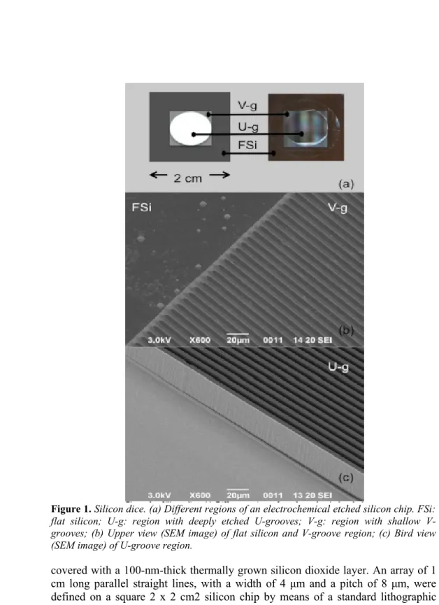
Figure 1. Silicon dice. (a) Different regions of an electrochemical etched silicon chip. FSi: flat silicon; U-g: region with deeply etched U-grooves; g: region with shallow V-grooves; (b) Upper view (SEM image) of flat silicon and V-groove region; (c) Bird view (SEM image) of U-groove region.
covered with a 100-nm-thick thermally grown silicon dioxide layer. An array of 1 cm long parallel straight lines, with a width of 4 μm and a pitch of 8 μm, were defined on a square 2 x 2 cm2 silicon chip by means of a standard lithographic step. Buffered Hydrofluoric Acid (BHF) etch followed by a Potassium Hydroxide
(KOH) etch were used to transfer the pattern in the silicon dioxide and in silicon substrate, respectively. The KOH etch formed full V-grooves used as initial seeds .for the following electrochemical etching step. Electrochemical etching in a HF-based solution ([HF]=5%:[H2O]=95% by vol.) was then used to fabricate deep regular trenches in the patterned substrate. The etching voltage Vetch was set to a constant value of 3 V for the entire etching process, while the etching current Ietch was set to an initial value Ietch0 = 23.21 mA and properly reduced during the process in order to get a constant width (about 5 μm) of the trenches throughout the entire etching depth. The etching time tetch=2100 s was chosen to fully etch 50 μm deep trenches.
After the electrochemical etching, a drying step aimed to the evaporation of the liquid filling the trenches was performed. After the fabrication process is completed, for each silicon chip (Fig. 1a) three regions with different morphology can be highlighted: i) a flat silicon area (FSi) all along the chip borders; ii) a KOH-etched region containing an array of 1-2 μm deep V-grooves (V-g) and iii) an electrochemically etched region, with circular shape and area of 0.64 cm2, consisting of an array of 50 μm deep U-grooves (U-g). Fig. 1 shows Scanning Electron Microscope (SEM) images of the three different regions, namely flat silicon and V-grooves in Fig. 1B, and U-grooves in Fig. 1c. The roughness of the ECM-fabricated surfaces was evaluated using a stylus profilometer (Veeco profilerwith vertical resolution of 0.1 nm), obtaining a typical peak-to-valley value not larger than 20 nm [16]. This value is in good agreement with the estimation obtained by best fitting the experimental reflectivity with theoretical spectra, calculated through fine modeling of the silicon structure, taking into account surface roughness, as detailed in [16]-[18]
A few silicon chips were cut in the direction parallel to the U-grooves to obtain two rectangular dice. A few rectangular dice were further cut in the direction orthogonal to the grooves to attain a pair of 1 x 1 cm2 square dice, in which U-grooves are open to the external environment not only on top but also on one side. Interaction among cells and silicon surfaces was investigated by placing each silicon sample in a separate well of 6- or 12-well plates, where cell culturing was performed. The smallest dice fitted in 2.2-cm diameter wells, whereas other dice were hosted in 3.5-cm diameter wells.
B. Cell cultures and reagents
SW613-B3 cells (from human colon carcinoma) were grown as monolayers in complete DMEM supplemented with 10% FCS, glutamine (4 mM), Na/pyruvate (2 mM), penicillin (100 U/ml) and streptomycin (0.1 mg/ml) (all reagents were from Celbio, Milan, Italy).
Human SV40-transformed fibroblasts MRC-5V1 and HeLa cells were grown as monolayers in complete DMEM (Lonza) supplemented with 10% Fetal Bovin
Serum (FBS), glutamine (4 mM), and gentamicin (50 μg/ml) (all from Sigma). Human SW480 primary colon adenocarcinoma cells (American Type Culture Collection, No. CCL-228) were grown as monolayers in complete RPM1 (Lonza) supplemented with 10% FBS, glutamine (2 mM), Hepes (25 mM) (all from Lonza) and gentamicin (80 μg/ml) (Essex Italia). Cells were grown at 37 °C in a humidified atmosphere containing 5% CO2, and trypsinized when confluent as previously described [31]. Cells (3x10⁵) were plated on sterilized micromachined silicon devices in 6- or 12-well dishes and incubated for 24 hours before fixing. Culture experiments were repeated several times by growing each cell line on all kinds of dice hosted in the suitable well. Preliminary experiments carried out on conventional glass slides and silicon flat samples allowed the selection of the proper culture time. In the range of 24-60 h, the 24 h span ensured a sufficient cell density with few cell overlapping and without the need to replace medium.
Cell culture was performed in standard and static conditions, with the final goal to have a sufficient number of cells in the testing area and, in turn, obtain a good cell density inside the gaps of the PhC. In such a way several sites will be available for evaluating the ability of the optical transducer in recognizing cell distribution, in future testing experiments with a fiberoptic readout setup.
C. Fluorescent assays
At the end of the incubation time, the multi-well plates were removed from the incubator. After the medium was aspirated and wasted, silicon dice were gently washed (twice) with a phosphate buffer solution (PBS) (0.1 M), finally replaced with cold (-20 °C) 70% ethanol (2 ml) for cell fixation. The plates were stored overnight at +4 °C. In order to evaluate the growth behavior and the cell morphology, the samples were stained with a combination of two fluorochromes for labeling both the nuclear DNA and the cytoplasm components. Propidium Iodide (PI) is the established DNA probe while Fluorescein Isothiocyanate (FITC) is the brilliant tag for primary amino groups of proteins. A mixture of dyes, (1 μg/ml) for PI and (0.1 μg/ml) for FITC, in PBS applied for 30 mins turned the cell-on-silicon samples suitable for fluorescence observation. In order to prevent sample drying during observation, the dice were gently washed in PBS and mounted with cover-glass. Fluorescence imaging was performed with an Olympus BX51 microscope with standard fluorescence equipment (HBO100 W/2 lamp). Fluorescence microphotographs were taken using an Olympus Camedia C-4040 digital camera. The increasing magnifications from 4X to 40X were routinely used to characterize and compare standard controls (glass slides) with silicon devices as well as to highlight results obtained in the different silicon regions. Fluorescence images were recorded with low magnification to show different areas of the silicon die while a higher magnification allowed more detailed imaging of cell morphology and fine organization of cells inside and over the silicon grooves.
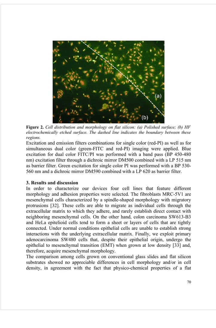
Figure 2. Cell distribution and morphology on flat silicon: (a) Polished surface; (b) HF electrochemically etched surface. The dashed line indicates the boundary between these regions.
Excitation and emission filters combinations for single color (red-PI) as well as for simultaneous dual color (green-FITC and red-PI) imaging were applied. Blue excitation for dual color FITC/PI was performed with a band pass (BP 450-480 nm) excitation filter through a dichroic mirror DM500 combined with a LP 515 nm as barrier filter. Green excitation for single color PI was performed with a BP 530-560 nm and a dichroic mirror DM590 combined with a LP 620 as barrier filter.
3. Results and discussion
In order to characterize our devices four cell lines that feature different morphology and adhesion properties were selected. The fibroblasts MRC-5V1 are mesenchymal cells characterized by a spindle-shaped morphology with migratory protrusions [32]. These cells are able to migrate as individual cells through the extracellular matrix to which they adhere, and rarely establish direct contact with neighboring mesenchymal cells. On the other hand, colon carcinoma SW613-B3 and HeLa epitelioid cells tend to form a sheet or layers of cells that are tightly connected. Under normal conditions epithelial cells are unable to establish strong interactions with the underlying extracellular matrix. Finally, we exploit primary adenocarcinoma SW480 cells that, despite their epithelial origin, undergo the epithelial to mesenchymal transition (EMT) when grown at low density [33] and, therefore, acquire mesenchymal morphology.
The comparison among cells grown on conventional glass slides and flat silicon substrates showed no appreciable differences in cell morphology and/or in cell density, in agreement with the fact that physico-chemical properties of a flat
crystalline silicon surface are close to those of standard glass slides. Cells were cultured also on flat silicon dice incorporating both lapped and electrochemically etched surfaces, to investigate the effect of surface roughness. In Fig. 2, a fluorescence microscopy image illustrates cell distribution on these surfaces. The dashed line indicates the boundary between the polished and electrochemically etched flat silicon surfaces. The image shows that cell morphology and density are similar on both regions, thus suggesting that the typical roughness of HF-etched structures does not affect cell growth.
This observation is in agreement with results reported in the literature relative to in vitro experiments, showing that stem and cancer cells retained their viability on the surface of porous silicon even with protrusions and depressions up to 100 nm [34]. As to the micromachined silicon dice, important and evident differences between the three regions exist, as confirmed by repeating the same experiment six times. The use of dice that incorporate three different regions allows for a direct comparison of the cell behavior between standard flat Si and V-grooves, already reported in the literature, with respect to the newly proposed deep U-grooves, since cells grow on the different structures at the same time and exactly in the same environmental conditions, thus eliminating spurious effects due to the typical biological variability observed from time to time or between different wells.
Figure 3. Fluorescence images relative to SW613-B3 cells. (a) Low magnification; (b) Cell morphology in flat silicon region; (c) Cell distribution in the region with V-grooves; (d) Cell distribution in the region with deeply etched U-grooves. The majority of the nuclei (PI-red) are “round”, typical of cells on top of the walls.
Figure 4. Fluorescence images relative to HeLa cells. (a) Low magnification; (b) Cell morphology in flat silicon region; (c) Cell distribution in the region with V-grooves; (d) Cell distribution in the region with deeply etched Ugrooves. The majority of the nuclei (PI-red) are “round”, typical of cells on top of the walls
Figure 5. Fluorescence images relative to SW480 cells. (a) Low magnification; (b) Cell morphology in flat silicon region; (c) Cell distribution in the region with V-grooves; (d) Cell distribution in the region with deeply etched U-grooves. Some of the nuclei (PI-red) exhibit an elongated shape, typical of cells grown inside the gap between walls.
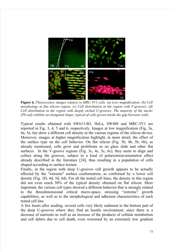
Figure 6. Fluorescence images relative to MRC-5V1 cells. (a) Low magnification; (b) Cell morphology in flat silicon region; (c) Cell distribution in the region with V-grooves; (d) Cell distribution in the region with deeply etched U-grooves. The majority of the nuclei (PI-red) exhibits an elongated shape, typical of cells grown inside the gap between walls. Typical results obtained with SW613-B3, HeLa, SW480 and MRC-5V1 are reported in Fig. 3, 4, 5 and 6, respectively. Images at low magnification (Fig. 3a, 4a, 5a, 6a) show a different cell density in the various regions of the silicon device. Moreover, images at higher magnification highlight, in more detail, the effect of the surface type on the cell behavior. On flat silicon (Fig. 3b, 4b, 5b, 6b), as already mentioned, cells grow and proliferate as on glass slide and other flat surfaces. In the V-groove regions (Fig. 3c, 4c, 5c, 6c), they seem to align and collect along the grooves, subject to a kind of polarization/orientation effect already described in the literature [24], thus resulting in a population of cells shaped according to surface texture.
Finally, in the region with deep U-grooves cell growth appears to be actually affected by the "extreme" surface conformation, as confirmed by a lower cell density (Fig. 3D, 4d, 5d, 6d). For all the tested cell lines, the density in this region did not even reach 50% of the typical density obtained on flat silicon. More important, the various cell types showed a different behavior that is strongly related to the threedimensional critical micro-space, stressing “extreme” growth capabilities, as well as to the morphological and adhesion characteristics of each tested cell line.
A few hours after seeding, several cells very likely sediment to the bottom part of the deep U-grooves where they find an hostile environment, since there is a decrease of nutrients as well as an increase of the products of cellular metabolism and cell debris due to cell death, even worsened by an extremely low gradient
caused by lateral closure of the gaps. The situation on the surface is different, since cells experience a better availability of nutrients and a better exchange with the environment. However, cells on top of silicon walls have a limited chance to proliferate and divide on a flat horizontal surface, having a width of a few micrometers. Once a few cells become attached on the top of some walls (with a very limited gripping surface), they are forced to explore the surrounding vertical surfaces in order to discover the “way to survive” and proliferate. To accomplish this environmental inspection, they start extending cytoplasm elongations towards the vertical surfaces, looking for a stable contact point or anchorage. Part of the cell body can be, therefore, moved in that direction and, finally, the cell can be found alive on the edge of a wall with part of its body extended inside the gap and adherent to the vertical surface of the wall. Once this cell is mature for duplication, this step can occur on the very limited flat surface on top of the wall or by exploiting the large vertical surface where it is already attached. Experimental results highlight that the capability of performing this sequence of events is strongly dependent on, and related to, the cell type. The first requirement seems to be the ability of a cell type to elongate parts of its body for finding contact points, which is a typical feature of mesenchymal cell lines; the second one is the capability to survive and proliferate in a narrow vertical space. Fluorescence microscopy images of cells grown on flat silicon (Fig. 3b, 4b, 5b, 6b) show that all the investigated cells lines exhibit their typical morphological figures demonstrating their ability to elongate the cytoplasm, to form bridges towards other nearby cells or simply to explore specific anchorages of the surrounding space. On the other hand, it is evident that the behavior between the tested cell lines is fairly different in the region with deeply etched U-grooves; MRC- 5V1 and SW480 cells grow preferentially inside the gaps, attached to the inner side of the silicon walls, whereas HeLa and SW613-B3 remain prevalently on top of the silicon walls where they tend to form colonies, as shown in Fig. 3d, 4d, 5d, 6d. This different behavior of the tested cell lines was found independent from the size of silicon chips. With regard to the maximum depth reached by cells, preliminary data obtained with fluorescence imaging using confocal microscopy show the presence of cell nuclei in the gaps until the depth of 15-20 μm from top. Images taken by scanning electron microscopy of the cross-section of devices, hosting SW480 and MRC-5V1 cells, confirm confocal microscopy data and, in addition, show cytoplasmic elongations that in some regions can also reach the bottom of the gaps.
We have thus demonstrated that mesenchymal types of cells are able to grow inside the gaps of a high aspect-ratio micromachined structure that is a one-dimensional photonic crystal device. Cells growing inside the gaps can potentially play the role of bioreceptors within the photonic crystal structure, which can be then exploited not just for cell culturing but, more interestingly, as optical
transducer, so allowing to monitor cellular activity in a three-dimensional microstructured environment. The first step towards the achievement of such an integrated cellular sensor is the demonstration, given in this work, that some cell types can actually grow inside these PhC structures. Although interesting data can certainly be obtained by fluorescence imaging, by exploiting the photonic crystal properties of such microfabricated structures we expect to obtain, in a nondestructive way, the vertical and horizontal (X-Y plane) distribution of the cells partially filling the three-dimensional space in the gaps, beyond the first silicon wall facing the fiberoptic tip. In fact, as already demonstrated in [18], spectral reflectivity of the photonic crystal in the 1.0 - 1.7 μm wavelength region, in orthogonal direction to the walls, can be detected with high spatial resolution by using a lensed fiber; these optical properties are known to be strongly dependent on the material (e.g. cells) filling the gaps.
4. Conclusions
We have performed investigations on the growth behavior of four different cell models (SW613-B3, HeLa, SW480, MRC-5V1) on silicon chips containing, side-by-side, regions with different micro-structural features (flat surface, shallow V-grooves and vertical, high aspect-ratio U-V-grooves). Results show that the cell behavior is similar on glass substrates (used as standard reference) and both polished and electrochemically etched flat silicon. In the regions with shallow V-grooves all cells tend to align along the V-grooves direction, a kind of polarization/orientation trend already described in the literature. In the regions with deep U-grooves, cells find an "extreme environment" where the available flat surface for anchoring on top of the silicon walls is in direct competition with empty deep gaps between adjacent walls, thus leading to a lower cell density. Cells probably find on the surface a better situation in terms of nutrients and fluid exchange than at the bottom. Less adherent epithelioid SW613-B3 and HeLa cells tend mainly to grow and form colonies on the top of the silicon walls. Once attached on top of the walls, cells could begin to explore the possibility to colonize also the vertical surfaces of the walls, at least in their upper portion. This is mainly accomplished by SW480 and even better by MRC-5V1 cells that show the ability of stretching their bodies in the vertical direction, thus obtaining sufficient grip, which represents a fundamental requirement for cell migration. The ability to invade the U-grooves nicely correlates with the characteristics of mesenchymal cells with respect to epithelial cells that are less favored. These
results envision the possibility to exploit the proposed high aspect-ratio three-dimensional microstructure, which features the optical properties of a photonic crystal material, incorporating the cell model as a cell-based label-free optical
biosensor for the identification of drugs interfering with the apoptosis and EMT processes, which plays a relevant role in cancer progression and tumor metastasis [35]. Future work will concern the possibility to directly detect changes of the optical properties of photonic crystal structures, induced by the presence and/or modification of cells inside the gaps, through in-plane measurements of spectral reflectivity, using a fiber optic setup. Aims of further researches will also be design, fabrication and testing of a lab-on-chip based on our results as well as studies and optimization of cell culture conditions in such a chip. Issues such as cell density, incubation time, flow rate of medium and all the requirements to have a “live-cell model” inside that chip will be taken into account when a closed device will be available.
Reference
_________________________________________________________________ [1] T. H. Park and M. L. Shuler, “Integration of Cell Culture and Microfabrication Technology,” Biotechnol. Prog., vol. 19, pp. 243–253, 2003.
[2] J. El-Ali, P. K. Sorger, and K. F. Jensen, “Cells on chips,” Nature, vol. 442, pp. 403– 411, 2006.
[3] Y. Tanaka, K. Sato, T. Shimizu, M. Yamato, T. Okano, and T. Kitamori, “Biological cells on microchips: New technologies and applications,” Biosens. Bioelectron., vol. 23, pp. 449–458, 2007.
[4] Y. Fang, A. M. Ferrie, N. H. Fontaine, J. Mauro, and J. Balakrishnan, “Resonant waveguide grating biosensor for living cell sensing,” Biophys. J., vol. 91, pp. 1–16, 2006. [5] Y. Fang, “Non-invasive optical biosensor for probing cell signaling,” Sensors, vol. 7, pp. 2316–2329, 2007.
[6] C. J. Choi and B. T. Cunningham, “Single-step fabrication and characterization of photonic crystal biosensors with polymer microfluidic channels,” Lab Chip, vol. 6, pp. 1373–1380, 2006.
[7] D. Dorfner, T. Zabel, T. Hürlimanna, N. Haukea, L. Frandsenb, U. Ranta, G. Abstreitera, and J. Finley, “Photonic crystal nanostructures for optical biosensing applications,” Biosens. Bioelectron., vol. 24, pp. 3688–3692, 2009.
[8] M. Lee and P. M. Fauchet, “Two-dimensional silicon photonic crystal based biosensing platform for protein detection,” Opt. Express, vol. 15, pp. 4530–4535, 2007.
[9] N. Skivesen, A. Tetu, and M. Kristensen, “Photonic-crystal waveguide biosensor,” Opt.
Express, vol. 15, pp. 3169–3176, 2007.
[10] Y. Zhao, X. Zhao, and Z. Gu, “Photonic Crystals in Bioassays,” Adv. Funct. Mater., vol. 20, pp. 2970 –2988, 2010.
[11] S. Sadoka, Optical properties of photonic crystals. 2nd ed. New York:Springer, 2005. [12] J. D. Joannopoulos, S. G. Johnson, N. Joshua, R. D. Meade, and J. N. Winn, Molding
[13] G. Barillaro, A. Diligenti, M. Benedetti, and S. Merlo, “Silicon micromachined periodic structures for optical applications at 1.55 μm,” Appl. Phys. Lett., vol. 89, pp. 151110-1–151110-3, 2006.
[14] G. Barillaro, V. Annovazzi-Lodi, Diligenti, M. Benedetti, and S. Merlo, “Reflection properties of hybrid quarter-wavelength silicon microstructures,” Appl. Phys. Lett., vol. 90, pp. 121110-1–121110-3, 2007.
[15] G. Barillaro, S. Merlo, and L. M. Strambini, “Band gap tuning of silicon micromachined 1D photonic crystals by thermal oxidation,” IEEE J. Sel. Top. Quantum
Electron., vol. 14, no. 4, pp. 1074–1081, July-August 2008.
[16] G. Barillaro, L.M. Strambini, V. Annovazzi-Lodi, and S. Merlo, “Optical Characterization of High-Order 1D Silicon Photonic Crystals,“ IEEE J. Sel. Top. Quantum
Electron., vol. 15, no. 5, pp. 1359–1367, September-October 2009.
[17] G. Barillaro, S. Merlo, and L. M. Strambini, “Optical Characterization of alcohol-infiltrated 1-D silicon photonic crystals,” Opt. Lett., vol. 34, no. 12, pp. 1912–1914, June 15, 2009.
[18] G. Barillaro, S. Merlo, S. Surdo, L.M. Strambini, and F. Carpignano, “Optical quality-assessment of high-order one-dimensional silicon photonic crystals with a reflectivity notch at λ~1.55μm,” IEEE Photonics J., vol. 2, no. 6, pp. 981-990, 2010.
[19] S. Surdo, L. M. Strambini, G. Barillaro, F. Carpignano, and S. Merlo, “Silicon micromachined photonic crystal integrated in an optofluidic microsystem,” in IEEE
Proceedings of International Workshop Biophotonics 2011, Parma, Italy, June 8-10, 2011,
paper ID 1785817.
[20] G. Barillaro, A. Nannini, and M. Piotto, “Electrochemical etching in HF solution for silicon micromachining,” Sens. Actuators A, vol. 102, pp. 195–201, 2002.
[21] G. Barillaro, A. Diligenti, A. Nannini, and G. Pennelli, “A thick silicon dioxide fabrication process based on electrochemical trenching of silicon,” Sens. Actuators A, vol. 107, pp. 279–284, 2003.
[22] Y. Torisawa, H. Shiku, T. Yasukawa, M. Nishizawa, and T. Matsue, “Multi-channel 3-D cell culture device integrated on a silicon chip for anticancer drug sensitivity test,”
Biomaterials, vol. 26, pp. 2165–2172, 2005.
[23] J. H. Yeon and J. K. Park, “Microfluidic Cell Culture Systems for Cellular Analysis,”
Biochip J., vol. 1, pp. 17–27, 2007.
[24] C. D. W. Wilkinson, “Nanostructures in Biology,” Microelectron. Eng., vol. 27, pp. 61–65, 1995.
[25] E. T. den Braber, J. E. de Ruijter, H. T. J. Smits, L. A. Ginsel, A. F. von Recum, and J. A. Jansen, “Quantitative analysis of cell proliferation and orientation on substrata with uniform parallel surface micro-grooves,” Biomaterials, vol. 17, pp. 1093–1099, 1996. [26] E. T. den Braber, J. E. de Ruijter, L. A. Ginsel, A. F. von Recum, and J. A. Jansen, “Quantitative analysis of fibroblast morphology on microgrooved surfaces with various groove and ridge dimensions,” Biomaterials, vol. 17, pp. 2037–2044, 1996.
[27] M. Nikkhah, J. S. Strobl, and M. Agah, “Attachment and response of human fibroblast and breast cancer cells to three dimensional silicon microstructures of different geometries,” Biomed. Microdevices, vol. 11, pp. 429–441, 2009.
[28] M. Nikkhah, J. S. Strobl, B. Peddi, and M. Agah, “Cytoskeletal role in differential adhesion patterns of normal fibroblasts and breast cancer cells inside silicon microenvironments,” Biomed. Microdevices, vol. 11, pp. 585–595, 2009.
[29] M. Nikkhah, J. S. Strobl, R. De Vita, and M. Agah, “The cytoskeletal organization of breast carcinoma and fibroblast cells inside three dimensional (3-D) isotropic silicon microstructures,” Biomaterials, vol. 31, pp. 4552–4561, 2010.
[30] J. S. Strobl, M. Nikkhah, and M. Agah, “Actions of the anti-cancer drug suberoylanilide hydroxamic acid (SAHA) on human breast cancer cytoarchitecture in silicon microstructures,” Biomaterials, vol. 31, pp. 7043–7050, 2010.
[31] S. Soza, V. Leva, R. Vago, G. Ferrari, G. Mazzini, G. Biamonti, and A. Montecucco, “DNA ligase I deficiency leads to replication-dependent DNA damage and impacts cell morphology without blocking cell cycle progression,” Mol. Cell. Biol., vol. 29, pp. 2032– 2041, 2009.
[32] E. D. Hay, “The mesenchymal cell, its role in the embryo, and the remarkable signaling mechanisms that create it,” Dev. Dyn., vol. 233, pp. 706–720, 2005.
[33] C. Ghigna, S. Giordano, H. Shen, F. Benvenuto, F. Castiglioni, P. M. Comoglio, M. R. Green, S. Riva, and G. Biamonti, “Cell motility is controlled by SF2/ASF through alternative splicing of Ron protooncogene,” Mol. Cell., vol. 20, pp. 881–890, 2005.
[34] L. A. Osminkina, E. N. Luckyanova, M. B. Gongalsky, A. A. Kudryavtsev, A. Kh. Gaydarova, R. A. Poltavtseva, P. K. Kashkarov, V. Yu. Timoshenko, and G. T. Sukhikh, “Effects of nanostructurized silicon on proliferation of stem and cancer cell,” Bull. Exp.
Biol. Med., vol. 151, no. 1, pp. 79-83, 2011.
[35] J. Yang and R. A. Weinberg, “Epithelial-mesenchymal transition: at crossroads of development and tumor metastasis,” Dev. Cell., vol. 14, pp. 818–829, 2008.