Chapter 2
Organic Light Emitting Diodes
2.1 Electroluminescent devices: state of the artElectroluminescence (EL) is the generation of light from condensed matter by electrical excitation.
The first observation of the electroluminescence phenomena date back to the 1936. Destriau et al. have been able to generate light from ZnS powders dispersed in an insulating material sandwiched between two electrodes generating high potential field.1 But the first electroluminescence observed in
organic materials was in 1963. Pope et al. have applied high voltage to an anthracene molecular crystal obtaining blue light emission.2 In 1965 Helfrich
and Schneider built the first organic‐based device by using electrolytic contact made with Ce sulphate and Na sulphyte to improve a balanced holes‐electrons charge injection.3 There were several draw‐backs preventing practical use of
these early devices. The main obstacles were the high operating voltage as a consequence of crystal thickness in micrometer range together with the difficulties in reproducible crystal growth as well as preparing stable and sufficiently well‐injecting contacts to them.
These investigations4 have established the basic processes involved in organic‐
injection type electroluminescence, namely injection, transport, capture and radiative recombination of oppositely charged carriers inside the organic material. Further steps towards applicable organic electroluminescent devices was made in the 1970s by the usage of thin organic films prepared by vacuum
vapour deposition or the Langmuir‐Blodgett technique instead of single crystals.5 The reduction of the organic layer thickness below 1 μm allowed to
achieve electric fields comparable to those which were applied to single crystals but now at considerably lower voltage. Apart from the morphological instability of these polycrystalline films there arose the problem of fabricating pinhole‐free thin films from these materials. These problems could be overcome in the early 1980s by the usage of morphologically stable amorphous films, as demonstrated by Partridge’s work on film of polyvinylcarbazole doped with fluorescent dye molecules. The development of organic multi‐layer structure considerably improved the efficiency of light emission by achieving a better balance of the number of charge carriers of opposite sign and further lowered the operating voltage by reducing the mismatch of energy levels between the organic materials and the electrodes. The consequence was the demonstration of organic light‐emitting devices (OLEDs) with the experiment of Tang and VanSlyke reported in 1987. They realized a sandwiched hetero‐layer structure (ITO/bis(triarylamine)/AlQ3/Mg:Ag), each layer a few nanometers thick, where
AlQ3, tris(8‐hydroxyquinolinate)Aluminium(III), is used for electron transport
and at the same time as an emitting layer, but unable to carry holes. In contrast, bis(triarylamine) was inserted to provide hole transport (Figure 2.1). N O Al N N O N N Figure 2.1: tris(8‐hydroxyquinolinate)aluminium(III) AlQ3 and bis(triarylamine). AlQ3 bis(triarylamine)
Therefore, recombination was largely confined to a region near the interface between both organic materials. So they could achieve high external quantum efficiency, 1%, remarkable luminous efficiency, 1.5 lm/W and brightness > 1000 cd/m2, operating voltage < 10V (Figure 2.2).6,7 Figure 2.2: Tang and VanSlyke OLED structure.
Some year after, in 1989, Burroughes observed the light emission from polymers with extended π conjugation as PPV [poly‐(p‐phenylene vinylene)] or from materials doped with fluorescent dye molecules as reported by Partridge
et al..8,9 But for a lot of time the general interest was focused on inorganic
materials obtained from III and V group as GaAs, GaP, InGaP, AlGaP until the more recent AlInGaP.
The ‘90 years knew a lively development of synthetic research to find new luminescent materials and to design new building devices techniques, so some device examples were the SOLED (Stacked OLED) proposed by Forrest and co‐ workers in 1997. With this approach in order to improve the RGB emission efficiencies, an independently controlled, three‐color, organic light‐emitting device was constructed with a vertically stacked pixel architecture. The 12‐layer device consisted of sequentially stacked layers of metal oxide, organic and metal thin films that allow for independent tuning of colour (RGB), grey scale, glass ITO diamine AlQ3 Mg:Ag hν
and intensity.10 From 1990s years, with the last OLEDs improvements, the
organic devices start to be introduced in the market.
Different techniques are employed to build an OLED device. It depend on the used organic materials end on witch device features have to be improved. The layers can be obtained with different techniques, high vacuum deposition techniques and solution‐based methods as solution casting or spin‐coater techniques. The research efforts to synthesis soluble molecules or polymers is due to better exploit the low cost solution‐based techniques. Friend’s innovation was built on the discovery of conductive polymers by Heeger, MacDiarmid, and Shirakawa in the 1970s, which earned them the 2000 Nobel Prize in chemistry.11 Recently RGB based polymers OLEDs were obtained by solution processes. Last generation of soluble polymers consists of functionalized oxyethane spyrobifluorene‐co‐fluorene blu, green and red emitting material. These polymer networks were obtained by photochemical treatments without important alterations of their luminescent properties. To lower production cost an alternative approach is the photopolymerization of thin liquid crystalline films bearing a luminescent core. So could be possible to exploit new OLED technologies by using standard lithographic techniques (ink jetting, screen printing) to realize pixels matrices displays in analogy with chip technologies.12
In many cases the research developed in the universities on this kind of studies meet the private market to generate new spin‐off and patents.13
The OLEDs technologies turn out advantageous and competitive in may aspects, it is possible to match the optoelectronic properties of the inorganic semiconductors with the typical properties of organic materials both oligomers, polymers or small organometallic molecules. Then high processability materials have to be synthesised. Solution‐based deposition techniques are chipper
methods than those employed for inorganic materials further it is possible to realize emitting layers for extended and flexible displays, extremely light and thin (1‐2 mm) if plastic support is used.14
An OLED display shows high brightness (100 cd/m2), high resolution and
contrast (100:1). Further, bigger viewing angle and luminous efficiency (max 180°, 16 lm/W) and less operating voltage than LC (Liquid Crystalline). These displays achieve 6000 hours of continuous operation.15
The photoluminescence and electroluminescence studies investigate also the intrinsic logic of photochromic substances. The absorption or the emission of quantum energy allow the possibility to exploit its as information bits, then not only to write but also to read the matter.16
The technological develop of applications with informative target, the growing mobility and aesthetic feature demand coupled with the growing necessity to use more efficient interfaces for information input and output could to twist some priorities. So the displays will not be any more considered peripheral units, but will gain the central unit importance, while the processor will be more and more considered a peripheral unit. These are the considerations on pervasive computing visions of J. Birnbaum of HP‐Laboratories.17
The OLED applications could be countless: from mobile phones to toys, from informative flexible flat panels to computers and TV displays; from wearable electronic to traffic signs or to house fittings. One of the applications could be the city fittings to limit the luminous pollution.
So organic electronic studies are intensely developed for the next‐generation light source and the backlight for flat panel display, energy‐saving, environmental protection, low thickness, and light weight are the well‐known requirements. To achieve theses requirements, light‐emitting diodes (LEDs),
electroluminescent (EL) devices, and organic light‐emitting diodes (OLEDs) are among the best candidates.
Light‐emitting diodes (LEDs) are based on wafers of inorganic materials. For the planar light sources, however, LEDs are not economically favourable due to the high cost of the light modules. While between the EL devices technologies, solid state light‐emitting devices are the results of recent investigation about electrochemical cells. Some examples of this kind of studies are based on solid thin‐film devices fabricated with ionic transition metal complexes as Ru(II), Os(II) and Ir(III) complexes. For instance [RuL3]2+ (L= 2,2‐bipyridine, bipy, 1,10‐
phenanthroline, phen, etc.) ion is an intrinsic semiconductor with a negligible
concentration of mobile electrons and holes at room temperature due to a large
HOMO‐LUMO (Highest Occupied Molecular Orbital – Lowest Unoccupied
Molecular Orbital) gap. [Ru(bipy)3]2+ carries a net charge 2+ which could be
compensated by two counter ions such as PF6‐ or ClO4‐. In a film these ions are
mobile at room temperature. The characteristic feature of the counter ions mobility is the redistribution trough the layer under the application of an
applied bias and assist the injection of electronic charge. Ion redistribution is
required in order to establish the mixed‐valent redox states needed for charge transport and light emission.
This electrochemical mechanism within layer influencing the turn‐on time voltage depend on the counter ion type involved in the process. So the technical limit until now is to reduce the time delay observed between voltage application and device response. This phenomenon is called charging time (time to achieve the maximum brightness) is associated with relatively slow counter ion redistribution. So to overcome these limits preconditioning techniques are taken in account as the use of solvents or ionic liquids; the employment of gradient of temperature: or the precharging techniques, using an initial high‐
voltage pulse. These studies are in the early stages but efficient devices can be made with air stable electrodes, in contrast to conventional organic light emitting diodes that require low work function cathodes.18‐20 Until now the EL
devices do not have sufficient light intensity for general lighting purpose. Therefore, OLEDs seem to be one of the most potent candidates as the next generation planar light source.
To increase the output power efficiency of these devices, two methods have been extensively studied either by the increase of internal quantum efficiency of the devices or by the improvement of output coupling efficiency. The internal quantum efficiency is generally enhanced by adjusting thin‐film structures of the devices. But the increase of internal quantum efficiency is very limited. Since the refractive indices of glasses and plastics are approximately 1.5, which is higher than air, only about 20% to 30% of the emitting light from OLED or EL devices can propagate into air. Therefore, there is a large space for improvement on the output coupling efficiency of the devices and many extensive researches are taking place on this topic.21,22
New trends in the use of transition metal‐ligand complexes for application in electroluminescent devices are gained industrial interest. The additional use of phosphorescent emitters, for instance iridium(III) or platinum(II) complexes, improve enormously the device efficiencies.
The phosphorescent emitters should exhibit very high phosphorescent quantum efficiencies. In particular iridium(III) complexes containing 2‐ phenylpyridine, benzoquinoline, 2‐phenylbenzothiazole and their derivatives (Figure 2.3), exhibit high triplet quantum yields due to the mixing of the singlet and the triplet exited states via spin‐orbit coupling.
A relatively short phosphorescence life time, significantly improves the performance of a phosphorescent material.
Figure 2.3: a) Different structure of amorphous iridium(III) phosphorescent emitters containing fluorine‐ modified phenylpyridine. b) Example of Ir(III) phosphorescent emitters containing 2‐(5‐ phenyl‐4H‐ [1,2,4] triazol‐3‐yl)pyridine; R= F, CF3 either in 3,5 position or 2,4 position or H.
OLEDs prepared with such heavy metal complexes are reported as the most efficient, with theoretical internal quantum efficiencies of 100% due to harvest of both singlet and triplet excitons.23 ‐ 26
Although the organic materials cost used in most thin‐film devices is low, in electronics the materials cost rarely determines that of the end product, where fabrication and packaging costs typically dominate. Hence, the successful application of this interesting materials platform will depend on capturing its low‐cost potential through the innovative fabrication of devices on inexpensive, large‐area substrates. This suggests that conventional semiconductor device fabrication technologies need to be adapted to the fabrication of large‐area substrate coated with organic circuits and to be compatible with the physical and chemical properties of organic/organometallic compounds.
Also, solids based on organic compounds are typically bonded by weak van der Waals forces that decrease as 1/R6, where R is the intermolecular spacing. This is
in contrast to inorganic semiconductors that are covalently bonded, whose strength falls off as 1/R2. Hence, organic electronic materials are soft and fragile,
whereas inorganic semiconductors are hard, brittle, and relatively robust when
exposed to adverse environmental agents such as moisture and the corrosive reagents and plasmas commonly used in device fabrication. The apparent fragility of organic materials has also opened the door to a suite of innovative fabrication methods that are simpler to implement on a large scale than has been thought possible in the world of inorganic semiconductors. Many processes involve direct printing through use of contact with stamps, or alternatively via ink‐jets and other solution‐based methods.27
Improving the fabrication techniques different type of OLED displays are realized. Passive or active matrix OLED displays are the two principal distinctions. In passive‐matrix display panels, the electrode material is deposited in a matrix of rows and columns. An OLED is formed at the intersection of each row and column. Display electronics can illuminate any OLED (pixel) in the array. A video image is created by sequentially scanning through all rows and columns, briefly switching on the pixels needed to display a particular image. An entire display screen is scanned (refreshed) in about 1/60 of a second. However, because of the high power consumption, passive‐matrix displays can be made with only a limited number of pixels.
Active‐matrix OLED displays are rapidly replacing passive‐matrix OLED displays for full‐colour applications. Active matrix OLEDs have an integrated electronic backplane as the substrate and are more suitable for high‐resolution, high information‐content videos and graphics. However, they are significantly
more expensive than passive‐matrix OLED displays. In an active‐matrix display, the array is still divided into a series of rows and columns, with a pixel formed at the intersection of each row and column. However, each pixel now consists of an OLED in series with a thin‐film transistor (TFT). The TFT is typically low‐temperature polycrystalline Si (LTPS) and controls the amount of current flowing through the OLED. LTPS transistors have high current carrying
capacity and high switching speed. The TFT in each pixel controls the brightness and the current flowing through the OLED. This continuous operation eliminates the need for the very high currents required in passive‐ matrix OLED displays. Resolution can be increased using single‐crystal Si substrates instead of LTPS. 28
The practical implementation of carbon‐containing semiconductors in electronic applications will ultimately be decided by the ability to produce devices and circuits at a cost that is significantly below that needed to manufacture conventional electronic circuits based on, for example, silicon.
Low‐cost fabrication processes will ultimately result in the ‘printing’ of large‐ area organic electronic circuits using roll‐to‐roll or web based methods, where low‐temperature deposition of the organics is followed by metal deposition and patterning in a continuous (Figure 2.4), high‐speed process analogous, perhaps, to processes used in the printing of documents or fabrics. Figure 2.4: Conceptual diagram of continuous manufacture of organic electronic devices.
Hence, a great deal of current research has focused on depositing films and patterning devices on a large scale (leading to ‘macroelectronic’ applications), avoiding the need for labour‐intensive techniques such as photolithography that today dominate the cost structure of conventional electronics.27 metal etch metal deposition organic deposition metal transfer metal deposition
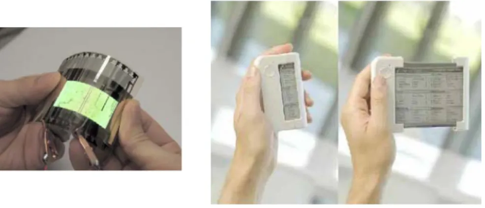
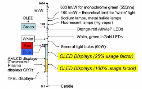
Colour flat panel electronic displays are light, durable and efficient and can be built on flexible substrates such as plastics and paper‐thin surfaces, for instance poly(ethylene terephtalate) (PET), creating displays that can be bent or rolled, so the next challenge is to product flexible displays (Figure 2.5). Figure 2.5: on the left, OLED on flexible substrate, source: Kyung Hee University; on the right, flexible display prototype.
A 128 x 64 pixel display (0:4mmx0:5 mm pixel size), operating at 100 cd/m2, was made on a standard PET tape (0.18 mm thick). The display was shown to bend to a radius of curvature of <1 cm.
Both polymers and low molecular weight molecules are useful foe this technology but still many efforts have to be done to overcome some technical limit (Figure 2.6) about the roll to roll manufacturing techniques and the encapsulation of this kind of displays.
Figure 2.6: performance target of flexible display.
with suitable physical‐chemical properties to be exploited for their flexible features (Figure 2.7). Figure 2.7: changing the display concept, from rigid to flexible. A proposed means is to lower the cost of producing flexible displays in a high‐ volume manufacturing environment by taking advantage of a unique attribute of flexible substrates relative to the traditional glass substrate. Such a manufacturing paradigm (Figure 2.8), compared to the traditional batch process (cluster tools and cassette transport), generally does not enable any enhanced product performance characteristics. Figure 2.8: Roll to roll production parameters. The target (Figure 2.9) is to reduce the form factor to obtain thin, lightweight, robust displays as, for instance, glass replacement for mobile displays or glass replacement for large TV and signals. These characteristics have to couple with
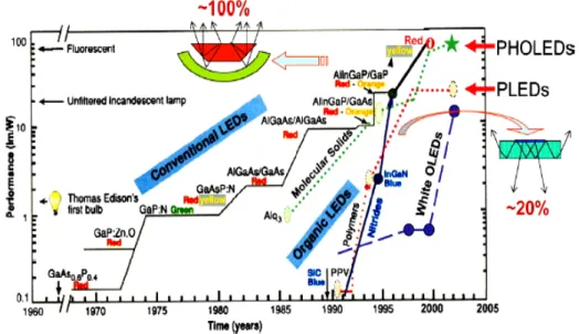
the flexibility so thin, robust and also conformable, rollable for instance roll‐out display for laptop; electronic paper, wearable displays.29 Figure 2.9: time line of developing R2R manufacturing. Contemporaneously in the latest years a lot of progresses were obtained in the develop of white OLEDs. The first one was produced by Kido and his colleagues in 1993. White OLED (WOLED) technology is drawing most attention due to its application for general solid‐state lighting and flat panel display backlighting of LCDs. In the fabrication of full colour display all three primary colours have equal importance but white light emission has drawn particular attention because any desired colour range can be achieved by filtering of white light. Further they can be candidate to overcome the tremendous amount of electricity consumed every year all over the world. In terms of total primary energy consumption, lighting accounts for about 20% of all the electricity produced. Fluorescent tubes and incandescent lamps are the frequently used traditional light sources and account for about 40% of the total electrical energy consumed. Incandescent bulbs turn about 90% of the energy into heat, while fluorescent do better by converting 70% of the energy they use into light. Incandescent lamps and fluorescent tubes have typical luminous efficiencies of 13 – 20 lm/W and 90 lm/W, respectively (Figure 2.10).
Figure 2.10: Comparison of the luminous efficiencies of several different lighting and display sources.
The lifetime may be defined as the average number of hours of operation in which the initial light intensity drops to 50%. The average lifetime of incandescent lamps is only 750–2500 h, while that of the fluorescent lamps is about 20000 h. Lifetime > 20000 h for several coloured OLEDs is repeatedly reported but today the typical lifetime of white OLEDs is less than 5000 h and efforts are still required to make white OLEDs reach the fluorescent tubes for efficiency and lifetime.
The efficiency of white OLED devices has increased very fast so could be considered as substitutes for conventional white light sources.
Typical emissive display image is assumed to require that only 25% of the pixels be lit at one time, resulting in an electrophosphorescent display efficiency of 2–10 lm/W, as compared to an active matrix liquid crystal display (AMLCD) efficiency of only 2 lm/W. Also, thin film electroluminescent (TFEL), plasma display, and inorganic LED efficiencies are shown for comparison.
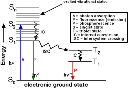
In Figure 2.11, the various OLED efficiencies noted are reported, as shown the best results obtained are for phosphorescent emitters in red, green, blue and white.31
Figure 2.11: the yearly progress in the efficiencies of conventional and OLED devices.
So in turn to save the world one should start getting rid of the light bulbs. In
addition, because OLED panels emit light only from the necessary pixels rather than the entire panel, power consumption is 20‐80% of that of LCDs. WOLEDs are promising devices to match the world demand of energy safe. Scheme 2.1: features and benefit of OLEDs technologies.
Since 1980, more than 6500 patents have been granted worldwide in this field brought of the knowledge and technologies improvement resumed in Scheme 2.1, with activity accelerating since the late 1990s.
In 2003, 17.3 million OLEDs were sold worldwide, and sales are expected to rise reaching 366 million in 2010.27 2.2 Generation of luminescence Molecules and metal chelates produce luminescence after photo‐excitation. Fluorescence (F) is a process in which a luminophore absorbs a suitable‐energy light quantum, hν, (a photon) to raise an electron from an occupied orbital to a higher energy vacant orbital, followed by the electron returning back to the original ground state energy level, and emitting a quantum of light, hν’, with an energy corresponding to the energy difference between the excited state and the ground state level, in such a way that the electron spin remains unchanged throughout the entire process. Thus, the molecule is all the time either in its ground or excited singlet states. This process, spin‐allowed transition (ΔS = 0) is
very fast. Luminescence lifetime is of the order of nanoseconds (10‐6 to 10‐9 s).
In other cases the molecule relaxes from the excited state, throughout a series of transitions called Internal Conversion (IC, <10‐12 s) , without emission of
radiation. The stored energy is dissipated under heat form.
Only in very rare cases, a much slower radiative relaxation of the molecule can occur in a solution at room temperature. This requires rather special molecule properties, which allow the excited electron to reverse its spin while it is transitioned to lower‐energy state, called a triplet state because the singly occupied electrons in different orbitals are now in a parallel spin this mechanism is called Intersystem Crossing (ISC). When the electron transitions to a ground state level its spin must be reversed again, spin‐forbidden
transitions (ΔS = 1), and therefore the time scale of the process is much slower
(10‐2 – 102s) than in the fluorescence process and is called phosphorescence (P).
The process which occur between the absorption and emission of light are usually represented in the Jablonski diagram, Figure 2.12, illustrating the different deactivation mechanisms.
Figure 2.12: Jablonski diagram.
Since the deactivation processes can be non‐radiatiative as in Internal Conversion or in Intersystem Crossing mechanisms, or quenching phenomena can occur due to the chemical environment of the excited molecule, the photoluminescence quantum yield
Φ
PL is defined as illustrated in Equation2.1.32 photons absorbed n photons emitted n ° ° = PL
Φ
Equation 2.1: photoluminescence quantum yield definition. hν hν’ hν’’2.2.1 Coordination compounds
Coordination compounds attract a lot of attention as chromophors. They exhibit luminescence which colour, then the emission wavelength, can be tuned by changing the coordinated metal centre or by introducing different kind of ligands in the coordination sphere or by changing the chemical properties of the substituents in the ligand structure. This versatility is largely applied in optoelectronic technologies. The optical properties of the metal complexes arise from the capability to absorb a specific wavelengths in the visible region of the electromagnetic spectrum. The optical absorption is due to transition depending on the separation of field‐ligands,
Δ
o, on the frontier orbitals. This separation depend on the character both of the metal centre and of the ligands as represented in the Molecular Orbital (MO) diagram of an octahedral complex reported in Figure 2.13. Figure 2.13: MO diagram of octahedral coordination compound. R Δo σ*M (eg) π M (t2g) p σL σ*M σ π π* πL π*L Metal Orbitals MC LMCT MLCT LC Molecular Orbitals Ligand Orbitals s d
The electronic spectrum provide a measure of the energy differences between the molecular orbitals which constitute the ground and the excited state of an excited electron associated to each electronic transition.
The excitated configurations can correspond to transitions involving molecular orbitals Metal Centred (MC) to exhibit d‐d transitions, or Ligand Centred (LC) in π−π* transitions. Light absorption can cause charge redistribution between
the metal and the ligands, the transition of an electron from an orbital based largely on the metal to an orbital based largely on the ligand, the absorption is described as Metal‐to‐Ligand Charge Transfer (MLCT) the opposite mechanism from an orbital based largely on the ligand to an orbital based largely on the metal is described as ligand‐to Metal Charge Transfer (LMCT).33
2.2.2 Energy Transfer Mechanisms
The absorption and the emission properties displayed by the chemical species are intensely exploited in blended systems or when its are covalently linked in assembled chemical structure bearing at list one chromophors. The molecules in the excited state can be involved in energy transfer mechanisms, when the emission spectrum of a luminescent molecules, called donor (D), overlaps with the absorption spectrum of another molecules, called acceptor (A). Reabsorption process called Resonance Energy Transfer involve dipole‐dipole interaction between D and A and other factors such as concentration and structure of the luminescent species. Two type of processes can occur:
1. the exchange mechanism (Dexter – type), which is a coherent transfer of an exciton, from D to A sites, is a short‐range mechanism that require orbital overlap therefore physical contact between donor and acceptor.
The rate constant of exchange energy transfer is expected to be sensitive to the nature of the linker connecting D and A. The donor‐acceptor exchange interaction are by the orbitals localized on the linker.
2. the coulombic mechanism (Förster – type) resonance energy transfer (RET), which consist in a through‐space induced dipole energy exchange dependent on the D−A distance and on the orientation of the emission transition dipole of D and the absorption transition dipole of A (orientation factor, κ2), this mechanism not require physical contact
between donor and acceptor. With a good spectral overlap integral and appropriate photophysical parameters the distance dependence allows energy transfer to occur efficiently over distances largely exceeding the molecular diameter (~60 Å).
The transfer efficiency between D‐A pairs at fixed distance can be calculated from the decay lifetimes τD, in the absence of A, and τDA in the presence of A
(Equation 2.2).32
E= 1‐ τ
DA/τ
D Equation 2.2: transfer efficiency between D‐A pairs. 2.3 ElectroluminescenceMolecular organic solid phase shows mechanical, optical and electrical properties different than covalent or ionic solids. The main feature of the organic condensed matter is the presence of the weak van der Waals interactions. So low interaction energies, low melting point, high compressibility, poor mechanical resistance, very low conductivity characterise the physical properties of this kind of solids. Organic molecules have fluctuant dipole moments depending on the electron temporary states that induce
multipole moments in the neighbouring molecules. So the interaction energy Udis, between the temporary charge separation and the induced electrical
moment, is a weak attractive force called dispersion forces. The formal description, reported in the Relation 2.1 :
U
dis(r) ∼ ‐ 1/r
6Relation 2.1: interaction energy. where r is the intermolecular distance, doesn’t depend on the dipole moment of the molecules. This low interaction allow only small changes in the molecular electronic structure, then although in the solid phase each molecule retain own individual electronic structure. The electronic structure an the possible conductivity mechanisms are generally described by the Band Theory. The electronic conductivity depend on the sign and the number of charge carriers and on their mobility trough the material. The external fused orbitals, containing the valence electrons of a virtual infinite set of atoms, generate two energetic separate bands that correspond to the bond and anti‐bond orbitals respectively. These two bands, defined valence band (BV) and conduction band
(BC), respectively are separated by an energetic interval (Figure 2.14).
Figure 2.14: schematic representation of the materials band structure; E is the Fermi level. BV BC EG EF EG > kT EG < kT
The electrical characteristics of the materials are determined by the values of this energetic band‐gap (EG) electron forbidden. If the valence band is partially full or if the two bands are superimposed, then the application of a small electric potential difference between two points of the solid will be sufficient to excite the electron towards the vacuum levels, so their increased mobility generate a current. This is the case of a conductive solid. In the case of insulating or semi‐conducting materials, the valence band is completely occupied so it is necessary to supply energy to the electrons at list equal to those that separate them from the conduction band.
In the intrinsic semi‐conductor the band‐gap energy is comparable with the thermic energy (kT), in the other cases the only thermal excitation is not enough to promote electrons in the conduction band. This is the Bands Theory model.34
The phenomenon of charge conductivity in organic solid is explained by the hopping model theory. When an electron in the conduction band of a crystalline insulator or semiconductor polarizes or otherwise deforms the lattice in its vicinity generate a polaron. The polaron comprises the electron plus its surrounding lattice deformation (polarons can also be formed from holes in the valence band). If the deformation extends over many lattice sites, the polaron is ʺlarge,ʺ and the lattice can be treated as a continuum. Charge carriers inducing strongly localized lattice distortions form ʺsmallʺ polarons.
So charge carriers in organic molecular crystals emerge not as free “bare” particle but “dressed” as polaron type quasi‐particles, surrounded by electronic as well as intra‐ and intermolecular polarization clouds called phonons. The electronic polarization is assumed to be a very fast process, several orders of magnitude faster than the typical (vibronic) polarization, or typical residence time, τh, of charge carriers on individual molecules.
molecular crystals the domination of molecular properties over the crystalline ones, caused by the weakness of van der Waals intermolecular interaction, lead to a marked tendency of localization at room temperature of charge carriers and excitons on the individual molecule of the crystal. In terms of the microelectrostatic approach the main contribution to the electronic polarization energy is provided by the charge‐induced dipole interaction of polarized, maily π‐electron, shells of neighbouring molecules. Thus, the interaction is long‐ ranged and the polarization cloud extend over about 104 or more molecules.
Singlet excitation energies En of individual molecules are of the order of several
eV. The typical electronic polarization decay time are τd1 ≈ ћ/Eexc and τd2 ≈ ћ/
ΔEexc respectively (where Eexc is the energy of the singlet excitation state and in
an ideal crystal Eexc ≡ En). Time τd2 is appreciably longer than τd1. The first very
fast decay time τd1 is equal to the standard electronic polarization time τe (τe ≈
ћ/Eexc)which is the shortest time needed for the formation of the electronic
polaron. While τd2 reflects the time scale of complete accommodation of the
virtual exciton cloud around the charge carrier. The relaxation of the virtual exciton cloud take place in all directions around the carrier.
The typical charge carrier hopping (residence) time is τh is several orders of
magnitude greater than the typical standard time of polaron formation, τh >> τe.
So hopping model take in account the conduction states of the organic solids as ionised states, then the neutral equilibrium configuration of the molecules became a ionic equilibrium configuration.35,36
2.3.1 Excited states generation
Organic solids are insulating material, amorphous molecular aggregates show resistivity values of the order of 1015 Ω cm. The presence of charge as electrons
is determined by injection mechanisms of them into the organic materials. So the hopping model take in account the device electroluminescent mechanism as electrodynamic equilibrium. In organic electroluminescent devices the charge injection from electrode is due to the an external electric field applied to the electrodes.
Different kind of injection mechanisms are taken in account, for instance the Richardson‐Schottky thermionic injection or Fowler‐Nordheim tunnelling. The injected charges migrate through the organic material with an hopping mechanism.
Each time the carriers are localized on different molecular site, so charge carriers can be described as polarons. Positive polarons, MP+, and negative
polarons, MP‐, could be described as holes and electrons adopting the
terminology used for the traditional semi‐conducting materials (Figure 2.15). Figure 2.15: hole and electron injection. These charge carriers migrating (Figure 2.16) into the material can recombine to generate an exciton, an electrically neutral entity. catode (+) electron hole anode (‐)
Figure 2.16: hopping mechanism. This unit named Frenkel exciton (Figure 2.17), is typically on the order of 1.0 eV and its life time is longer than the normal excited state so they can diffuse into the material. When a materialʹs dieletric constant is very small, the Coulomb interaction between electron and hole become very strong and the excitons tend to be much smaller, of the same order as the unit cell so the electron and hole sit on the same cell. Excitons could decay with radiationless mechanism, or they could localize on a minimum energy site interacting with a luminescent molecule of the material.
The polarons recombination into the Frenkel exciton generate the luminescent molecule excitation due to an energy transfer mechanism.
Figure 2.17: exciton formation and exciton relaxation mechanisms. After an electron‐hole recombination event, the newly created electronic excited state has different route to decay. In addition to losing its energy by collision or photochemical reactions, the excited state can undergo internal conversion or intersystem crossing to a different spin state. Both singlet and triplet excited states are present in the material. Due to spin statistics three times more triplet (1‐α) than singlet states (α) are produced from electron‐hole recombination in deep trap free material (Scheme 2.2).37 Scheme 2.2: exciton decay and spin statistics. acceptor excited state
exciton
energy transfer e + hS
α = 1/4 1‐α = 3/4T
2.4 OLED structure
Organic light emitting diodes are thin‐film multilayer devices, as illustrated in Figure 2.18, in which active charge transport and light emitting materials are sandwiched between two thin layered electrodes, of which at least one must be transparent to light in order to observe light emission from the organic layer. Generally an indium tin oxide (ITO)‐coated glass substrate is used as anode, featuring high work function (~4.8 eV) and low sheet resistant (~20 Ω/□), while the cathode is a low work function metal such as Ca, Mg, Al or their alloys, for instance Mg:Ag, Li:Al, in order to guarantee efficient electron injection.
An organic layer with good electron transport (ELT) and hole blocking properties is typically used between the cathode and the emissive layer. Similarly a hole transporting layer (HTL) and an electron blocking layer (EBL) are typically used between the anode and the emissive layer. Figure 2.18: multilayer OLED structure.
If an external voltage is applied at the two electrodes, electrons are injected from the cathode and holes are injected from the anode into the organic layer beyond a specific threshold voltage depending on the organic material employed. HTL Anode EL Glass Substrate hν ETL Cathode
Under the influence of an external field charge carriers migrate in opposite directions and are driven to the emissive zone (Figure 2.19). If a hole and an electron encounter one other while drifting through the organic layer they can form excitons: excited singlet and triple states. The singlet state may relax radiatively. Since most common organic semiconductors are intrinsic p‐type conductors and therefore are better suited to transport positive charges, electron and holes usually recombine in the immediate vicinity of the cathode causing limited lifetime and efficiencies. So multilayer OLEDs structure, in which electron and hole transport are performed in different materials (ETL, HTL, EBL) overcome the described technical problems.
A suitable combination of charge‐transporting and emitting materials in layered devices reduces the energy barrier for the injection of the charge carriers and acts as a blocking layer against the injection of either holes or electrons from the adjacent layer and their subsequent escape from the device. Figure 2.19: representation of charge carrier recombination.
Any OLED have to perform different essential requirements. The cathode material work function have to match the organic LUMO level while the anode material work function have to match the organic HOMO level in order to obtain an effective charge injection and charge balance. Good electron and hole Metal Cathode Glass ITO HTL ETL v exciton EL hν
transport through device have to be realized with the opportune choice of the organic materials, so to posses a suitable ionization potential and electron affinity for energy level matching for the injection of charge carriers at the interfaces between the electrode /organic material and organic material/organic material.
OLEDs structure have to be built carefully, to avoid any defect responsible of dark spots and leakage currents. Then the organic materials have to be suitable to the formation of a uniform film without pinholes. Morphological, thermal, electrochemical and photochemical stability is required. The electroluminescent material have to be characterized by highly luminescence. An other important physical feature is to allow minimal internal reflection through refractive index matching between layers and to permit the formation of uniform, transparent amorphous thin films by deposition, spin casting or sputtering methods.
The ideal OLED can be achieved with the suitable combination of the different layers by choosing the opportune materials. In contrast to inorganic materials that consist of covalent or ionic bonds of atoms over the entire expanse of solids, organic materials are based on independent molecules and characterised by weak intermolecular interactions. Therefore, designs of organic materials can be readily performed on the molecular level. In particular, organic π‐electron systems have received attention as potential photo‐ and electro‐active materials. The right combination of different materials an the device architecture improve the device performance to achieve better lifetime, power efficiency, operational stability.38,2
2.4.1 Cathode
Charge injection into electroluminescent layer depend on the metal work function and on the energy barrier at metal/organic layer interface. Then for better electron injection low metal work function are desired. These properties measure the electron tendency to escape from the metal surface. Low work function metal is highly desirable to facilitate the injection of electrons. The attempt to use Ca, K, and Li for effective cathode materials revealed that they exhibit poor corrosion resistance and high chemical reactivity with the organic medium. Thus, a variety of low work function metal alloys such as Mg–Ag and Al–Li are used for cathodes. For example Mg–Ag with a volume ratio of 10:1 is commonly used as a low‐work function electron‐injecting cathode on AlQ3. The
addition of Ag into Mg considerably improves its chemical stability in the atmosphere and increases its sticking coefficient onto AlQ3 upon deposition.6,7
Alkali compounds have been combined with a capping Al layer, as protective layer, to form an efficient electron injector.
With an optimal thickness of 0.3–1.0 nm, both voltage reduction and efficiency enhancement were observed for Li2O, LiBO2, K2SiO3 or Cs2CO3. Alkali
compounds were believed to decompose during deposition and produce Li2O,
K2O, and Cs2O at the AlQ3/Al interface, respectively. As compared to thermally
evaporated Li–Al, device performance.39,40
An effective Al cathode for OLEDs could be constructed by interposing a thin (0.1–1.0 nm) LiF layer between Al and AlQ3, despite its high work function.
Devices with the bilayer electrode showed significantly better I–V characteristics and higher EL efficiencies than that with a standard Mg:Ag cathode. The cathodes have better chemical stability against atmospheric corrosion and are compatible with Si device processing.41,42
2.4.2 Anode
It has been known for many years that indium oxide, in thin film form, is a transparent conductor, typically passing over 90% of visible light and displaying electrical resistivity between 10‐5 e 10‐6 Ω m. These properties have
led to a wide range of technical applications both in coating glass for energy‐ efficient windows or burglar alarms and as transparent elements in optoelectronic devices such as solar cells. Physically these properties result from its being an n‐type semiconductor with a band gap of between 3.5 and 4 eV. Oxygen vacancies provide electrons by acting as doubly charged donors, and films are generally sufficiently oxygen deficient that the electron gas in the conduction band is degenerate. Films are often prepared with a small proportion (5 to 15%) of tin oxide to form indium tin oxide (ITO) as this has been observed to increase the carrier concentration. The tin is commonly believed to provide electrons by substituting for indium and acting as a singly charged donor on an indium site.43
Oxidation of the ITO surface by O2 plasma, CF4/O2 plasma or UV ozone
treatment can reduce the carrier injection energy barrier, remove residual organic contaminants and get its work function up to near 5 eV which is still about 0.5 eV lower than most of the HOMO of the hole‐transport materials.
2.4.2.1 Non ITO anode.
Relatively few materials have been explored as alternatives to ITO as OLED anodes. ITO has the virtue of optical transparency, but it is not a well‐controlled material. Several alternative materials have been recently examined as anodes, however all suffer from some unfavourable characteristics.
Fluorine‐doped tin oxide. Both Ge‐doped ITO and fluorine‐doped tin oxide (ITO) have been used as an alternative to ITO for hole‐injection in PLEDs.44,45
Al‐doped zinc oxide (AZO). Unlike ITO, zinc oxide is a non‐toxic and inexpensive materials. It is an n‐type semiconductor with a bandgap of approximately 3.3 eV at room temperature. Zinc oxide doped with group III elements shows stable electrical and optical properties. Al‐doped zinc oxide films have low resistivity and good transmission in the visible region, comparable to ITO films.46 Transparent conductive oxides (TCO). Cui et al.
reported initial observations on the implementation of four new highly transparent, high work function TCO materials as OLED anodes: Ga0.12In1.88O3
(GIO), Ga0.08In1.28Sn0.64O3 (GITO), Zn0.5In1.5O3 (ZIO), and Zn0.46In0.88Sn0.66O3 (ZITO).
Besides exhibiting high electrical conductivities and broad, outstanding optical transparencies (>90%), the TCO films possess unusually high work functions (5.2–6.1 eV versus 4.5–4.7 eV for ITO).47
2.4.3 Electroluminescent materials
The basic requirements for organic electroluminescent materials are the the ability to transport charges towards an electrode and to have high luminescent quantum yield. A wide variety of organic or metal‐organic compounds are under investigation in order to optimize the device performances. The electroluminescent materials can be described in three main classes: dopant emitters, polymers, low molecular weight compounds.
2.4.3.1 Dopant emitters
Dopant emitters are highly organic fluorescent dyes in particular in the solid state. This kind of molecules are intensely exploited in many industrial fields. Their synthetic versatility is interesting feature to be applied in different organic systems as blend layers, in order to enhance electroluminescent performance as quantum efficiencies and lifetimes.
Condensed aromatics, porphyrins, coumarin or quinacridone derivatives are some examples of this widely used compounds. 48 One of the key developments
in the advancement of OLED display technology can be attributed to the discovery of the guest–host doped emitter system but at same time of the main problem is the film instability due to crystallization and phase separation which determine self‐quenching phenomena. 2.4.3.2 Polymers
Conjugated polymers are organic semiconductors with delocalized π– molecular orbitals along the polymeric chain such as polyacetylene (PA), poly(p‐phenylene) (PPP), poly(p‐phenylenevinilene) (PPV), poly(3,4‐ thylenedioxythiophene) (PEDOT) and their derivatives,49 are under intensely
investigation. The first conjugated polymer used for fabrication of an OLED was PPV. The incorporation of PPV into OLEDs is typically performed via a soluble precursor polymer that is spincast into thin films and converted to PPV by thermal treatment. In 1991, Heeger and Braun reported a red‐orange emitting OLED based on the unsymmetrically substituted soluble PPV derivative:poly(2‐nethoxy‐5‐(2‐ethylhexyloxy)‐p‐phenylenvinylene) (MEH‐ PPV) as shown in Figure 2.20.
O H3CO n Figure 2.20: MEH‐PPV
The introduction of substituent into the skeleton generate a new class of PPV polymers with modified electronic properties and enhanced solubility in organic solvents. Main chain conjugated polymers contain random dispersed defects leading to a statistical distribution of luminophore length. In contrast oligomer allow strict control of the effective conjugation length. The advantages of these compounds is the possibility to obtain thin film from solution‐based process. Taking advantage of both the processability of polymers and the defined optical and electrical properties of low molecular weight materials, defined charge transporting and/or emissive chromophors have been incorporated as conjugated main chain segments into a polymeric backbone or have alternatively attached as pendant groups to a non conjugated polymer. The polymeric nature yield amorphous films and warrants morphological stability, on the other side this approach ensures control of the conjugation length and the emissive colour, avoiding non emissive relaxation due to π‐stack formation.50
2.4.3.3 Low molecular weight compounds
Amorphous low molecular weight, small organic semiconductors may exhibit isotropic properties as well as homogeneous properties due to the absence of grain boundaries as in single crystals or liquid crystals. In contrast to polymers they are pure materials with well defined molecular structures and definite molecular weights without any distribution. Most the electroluminescent metal chelates contain ions belong to the II and III Group of the periodic table. They exhibit often strong fluorescent emission coupled with interesting molecular structure suitable to obtain charge transport ability and mofphologycal stability. The molecular design involve small common chelating ligands N,N, C,N, O,O and O,N as 8‐hydroxyquinoline and its substituted derivatives, phenantrolines or phenylbenzimidazoles. Triplet emitter as Iridium or lanthanide complexes are new synthetic target to collect the maximum OLED efficiency.51
2.4.4 Electron Transporting Layer and Hole Transporting Layer
Charge injection into the organic material is generally not balanced and to overcome this limit, then to enhance device efficiency and stability, different organic layer are stacked together in order to accomplish different kind of functions. Different “families” of organic molecule with a wide range of molecular weight and moreover with branched molecular structure to enhance the film stability were synthesised. This is the main approach to prevent crystallization, then degradation, so to design of materials with high glass transition temperatures that enable the preparation of high quality, morphologically stable and amorphous films. Electron transporting material reveal high electron affinity and mobility and exhibit large ionization potential
for hole blocking. Many metal chelates, in particular AlQ3 (Figure 2.21) exhibit
interesting electron transport properties and morphologically stable thin film upon vacuum deposition. N O Al N N O Figure 2.21: tris(8‐hydroxyquinolinate) alluminium(III), AlQ3
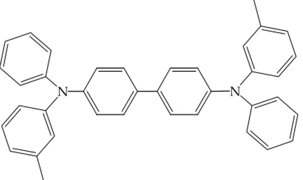
Another class of interesting electron transport materials are oxadiazole derivatives. Due to its extremely low hole affinity, 2‐biphenyl‐4‐yl‐5‐(4‐tert‐ butylphenyl)‐1,3,4‐oxadiazole (PBD) (Figure 2.22), has been widely used as hole blocking then electron transport layer. O N N Figure 2.22: 2‐biphenyl‐4‐yl‐5‐(4‐tert‐buttylphenyl)‐1,3,4‐oxadiazole, PBD. Numerous materials have been developed as hole transport layer. Triarylamine derivatives have gained importance due to their ability to be vacuum deposited and their high hole drift mobilities. The amine derivative that has been widely used as hole transport layer is TPD (N,N’‐diphenyl‐N,N’‐bis(3‐methylphenyl)‐ 1,1’‐biphenyl‐4,4’‐diamine), illustrated in Figure 2.23.
N N
Figure 2.23: TPD (N,N’‐diphenyl‐N,N’‐bis(3‐methylphenyl)‐1,1’‐biphenyl‐4,4’‐diamine)
The propensity of simple triarylamines to crystallize on aging is one of the main reason of degradation in OLED. Vacuum deposited TPD was found to crystallize at ambient temperature after a few hours. A strategies are to enhance morphological stability of the thin layer obtained with these molecules was to introduce iperbranched substituents or to synthesis oligomeric triarylamine. Charge injection was found to be facilitated when the hole transport layer is inserted close to the anode. So be cause of the high hole‐carrier drift mobility, the threshold voltage became accessible.52,2
One of the widely used polymers for promoting hole injection is poly(3,4‐ ethylenedioxythiophene)–poly(styrene) known as PEDOT/PSS (Figure 2.24) which has been found to be useful in a hybrid OLED architecture combining both the advantages of polymer LED and multi‐layered small molecule OLED. PEDT/PSS is an aqueous gel dispersion. The hydrated gel particles are formed by PSS interlinked by PEDT chains. Like CuPc, PEDOT/PSS as hole injection layer can smooth the ITO surface, reducing the probability of electrical shorts, decreasing the turn‐on voltage and prolonging the operation lifetime of the device. One of the potential drawbacks of using PEDOT/PSS is its acidity which could get as high pH as ∼3.
Figure 2.24: poly(3,4‐ethylenedioxythiophene)–poly(styrene) 2.4.5 Encapsulation After deposition of the organic and cathode layers, the display is encapsulated. The stability of device is one of the most important aspect in the OLEDs performances. The degradation of devices can occur both during operation of devices and during storage. The mechanisms of the degradation depend on the formation of non‐emissive dark spots in the metal/organic interface. It is proposed that a majority of dark spots are caused by the formation of metal oxides or hydroxides at the metal/organic interface. Moisture is thought to come through pinholes in the cathode surface. If the device is in ambient air, increasing the moisture will accelerate the formation of dark spots.53
Encapsulation is accomplished by bonding a sheet metal canister containing an alkaline earth oxide desiccant (typically CaO or BaO) to the substrate glass using a commercially available UV cured epoxy. Encapsulation prevents or limits the enlargement of dark spots and edge growth. Similar to darks spots caused by pinholes in the cathode, edge growth results from moisture penetrating below the cathode at the discontinuity created by the pillar and leads to a reduction in the emitting area of the pixel. A simple calculation indicates that at 20 °C and 60% moisture it approximately takes 4 days to
transmit 4 mg of H2O through a 1 mm wide and 40 mm thick adhesive layer.
Such amount of water is sufficient to form 3 nm of Al2O3 provided that the
OLED has an Al cathode with an area of 25mm x 25 mm. Therefore, desiccants are required to absorb water that permeates through the adhesive seal.54 In Figure 2.25 an example of encapsulated devices. Figure 2.25: Cross‐sectional view of an encapsulated OLED.
2.5 Devices physic
2.5.1 Device quantitative measurements
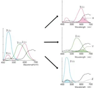
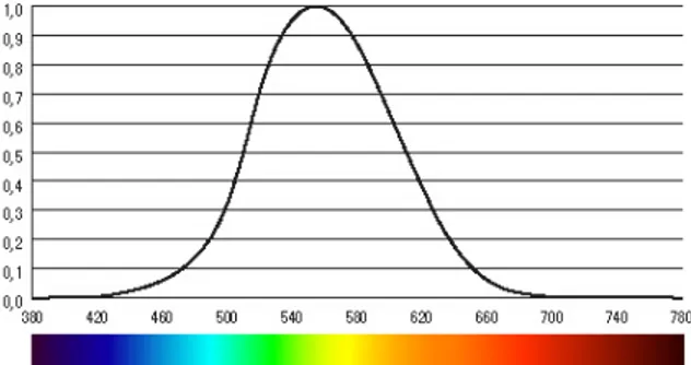
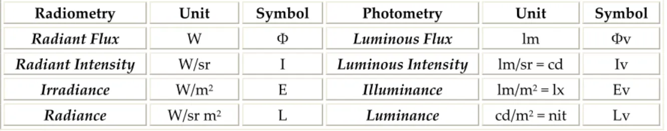
To have an accurate quantification of OLED efficiency it is necessary to know some basic concepts about radiometry and photometry because of the destination of organic devices is to be applied in display, so the pixels quality is also due to their colours, luminosity and intensity. The estimation of these properties need to take in account the eye response described by the photopic (light adapted) luminous efficacy that represent the photosensitivity of a “standard” human eye, and this is a further complication introduced by the fact that OLEDs destination is to interface with the human eye perception. Luminous intensity and other derived quantities are not objective physical quantity but depends on the physiology of the human eye, especially its sensitivity to light of different wavelengths 555 nm green‐yellow, 400 nm blue, 700 nm red, then colour matching functions x(λ), y(λ), z(λ), are used to represent the relative intensity of R (red), G (green), B (blue) primary colour perceived (Figure 2.26).