Chapter 3
V
ERIFICATION AND
V
ALIDATION
F
LOW IN
M
IXED
S
IGNAL
D
ESIGN
3.1 New challenges with mixed/signal design
In the last few years electronic market has pushed towards the development of products characterized by low cost, low power low area occupation and subject to a short time to market. These strict requirements have forced companies to aim towards the development of devices which integrates both digital controls and analog conditioning on a single chip [58][59][60].
In literature we can find a wide spectrum of mixed signal circuits whose application fields range from computers and peripherals to infotainment market. All applications based on sensors, especially ones that are based on MEMS devices are oriented to the use of complex mixed signal sensor interface. For example the automotive market is tended towards embedding an increasing number of sensing activities on a vehicle which are supported by performing electronic for analog signal detection, complex digital elaboration and final analog conditioning.
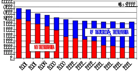
Consequently, as a matter of fact, the number of SoCs that have critical analog/mixed-signal content has reached roughly the 70% see Figure 3-1.
This new trend towards integration of complete systems on single silicon creates new problems and requires considerable resources to be applied to the development of new design concepts.
0 1000 2000 3000 4000 5000 6000 7000 8000 9000 10000 1995 1996 1997 1998 1999 2000 2001 2002 2003 2004 2005 2006 IBS 2001
Mixed-Signal
Digital
0 1000 2000 3000 4000 5000 6000 7000 8000 9000 10000 1995 1996 1997 1998 1999 2000 2001 2002 2003 2004 2005 2006 IBS 2001Mixed-Signal
Digital
Figure 3-1: Mixed Signal on overall SoC(%). Source Cadence.
The traditional approach for complex system composed by analog and digital IPs consists in partitioning the design at system level after a difficult architecture space exploration, from this point the design of the analog section and the digital section is carried out in two separate directions.
Furthermore the approach for developing the design of the digital part differs from the one of the analog part: the digital design flow is typically top-bottom featuring a continuous checking of alignment with specification and with global structure. On the other hand the analog design flow is more frequently bottom-up, thus not allowing a continuous cross-check between simulation and system level specification with limited feedback information from bottom analysis to top level. This aspect is related to the enormous time and the convergence problems that an analog SPICE simulation of the whole system would produce.
This different approach of the analog design flow from the digital one can lead to not completely tested final assembly. Problems are likely to arise especially on the interface between digital and analog section causing bugs difficult to highlight: any fault due to a wrong interaction between the analog and the digital section, or just inside the analog section can result in very expensive production delays[61][62][63].
A complete system simulation is therefore mandatory before an asic can reach tape out. Only by the means of a whole system simulation the designers can have the assurance that major problems on the connection between the analog and digital parts
are solved, and all interactions between the two different domains has been tested, thus avoiding most common bugs (e.g. bus exchanged, wrong connections, reference exchanged)
In order to perform simulations of the whole system the adoption of a hardware description language oriented to mixed signal design is mandatory. We have chosen the VHDL-AMS [64][65][66][67], (instead of Verilog-AMS [68]) guided by the better compatibility with available EDA tool suite [65]
The main challenges to create an efficient environment for system simulation and modelling of mixed signal SoC involving several hundreds of macro-blocks can be highlighted in: modelling the macro-blocks with the minimum set of details for fast top level functional simulation; guaranteeing the coherency of pinout and connectivity between the model and the real system; and performing these steps in a easy, quick and safe way.
3.2. System Verification Flow
To answer the strict requirements of the industrial market and to meet these requirements a semi-automatic verification flow has been developed. The verification flow is based on behavioural modelling of the whole analog part of a mixed signal IC.
The proposed verification methodology is described in Figure 3-2. The flow starts from single full-custom schematic: an automatic script (create_model.csh) generates a model template which contains the basic structure for the model of the full custom cell. The automatic generation of the architecture assures pin-out coherency regarding to the original cell, however a crosscheck can be done to fix eventual problems.
The VHDL-AMS model for full custom top is assembled linking all the semi-automatic generated model of the full custom cell by the means of a script (create_net.csh) which reads the Cadence™ top schematic and changes it into a verilog hierarchical netlist linking all the VHDL-AMS models. The script assures the designers to gain the exact connectivity coherent to the full custom top schematic, furthermore the generated netlist can detect a missing link or a missing model to refine the modelling and verification flow.
The model of the TOP analog section can be linked to the VHDL code (regarding the chip’s digital section) and the verilog PAD models for top level verifications of the whole system. Furthermore also the sensor can be modelled in VHDL-AMS, thus allowing the designers to have complete simulation of the whole application.
Full custom IP Create_model + manual modification VHDL-AMS modeling Full custom TOP Full custom TOP integration Coherency check VHDL-AMS IP model Create_net TOP connection extraction VHDL-AMS model for full custom TOP
Stimuli
Full custom standard verification
Stimuli
Full System Verification
UART Full custom TOP model Digital and Pads Sensor model
Figure 3-2: System Verification flow
The behavioural model of an analog macro block is an abstract, representation that can be simulated, which inherits the characteristics of most interest to the designer to be verified while suppressing physical detail irrelevant for top level behavioural simulation [69] in order to not overload the simulator avoiding long time consuming simulation with critical computational burden and convergence problems. However the VHDL-AMS model accuracy has to guarantee a sufficient precision for system level simulation and for detecting common top level connection bugs. In order to standardize the model schematic architecture and for helping the designers we have implemented an automatic generation of a model template common for all full custom cells which match the system requirements.
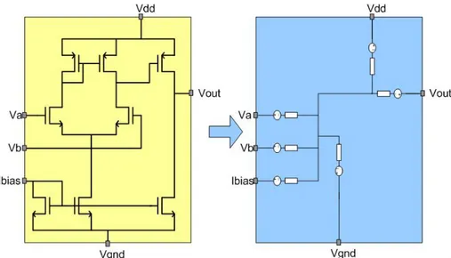
In Figure 3-3 we can observe an example of model generation for a simplified amplifier: is a circuit’s equivalent of the original transistor-level block, in which the designer can modify properly the value of internal parameters and functions.
In order to ensure the pin out coherency between the model and the original block, for all the analog cells, the models have been created semi-automatically, by means of a set of scripts, and then customized by the designer according to real behaviour of the analog cells.
Figure 3-3: Generic Analog Block and its Simplified VHDL-AMS Model
3.3. VHDL-AMS modeling flow
The high system complexity related to mixed signal design and the strict requirements of reliability to guarantee an exact matching of the VHDL-AMS model with regard to the relative schematic pin-out has forced to develop a semi-automatic flow for model generation that can assure pin-out compatibility and furthermore provides a standardisation for the model architecture and the controls related to each connection node.
i. VHDL-AMS model generation
In order to satisfy connectivity consistency, we have decided to use the Cadence™ Virtuoso command “create cellview from cellview” [70] to obtain, starting from the original schematic, a text file in which is contained the respective pin-out. This command is automatically executed by the create_model.csh script that requires as input just the name of the analog cell to be modelled, and the library in which the respective cell is instanced. This text is then post-processed with a C++ program that generates effectively the VHDL-AMS template ready to be compiled and simulated, plus a Verilog wrapper. This Wrapper in Verilog language absolves the function to restore pinout names case as it is on the schematic for model instance, in order to overcame the
missing case sensitive feature intrinsic of the VHDL-AMS (while the Verilog is case sensitive).
The C++ routine while executing asks the designers the nature of each pin to discriminate if the pin is related to analog purpose or to digital and if input or output may be specified. In case of an analog pin, it is declared inside the VHDL-AMS model as a electrical terminal, on the other hand if the pin is digital, it is declared as a std_logic pin.
The routine also asks for a reference, if exists, to be indicated in order to select the ground terminal to which every other analog terminal is referred.
The VHDL-AMS model can be used for analog, digital or mixed signal simulations, therefore to prevent any duplication the model, and the Verilog wrapper are instantiated in the analog environment and are automatically mirrored in the digital database, (since usually the digital simulation environment is different from the analog one) to prevent from duplication and any discrepancy between the analog and digital database.
ii. Model template structure
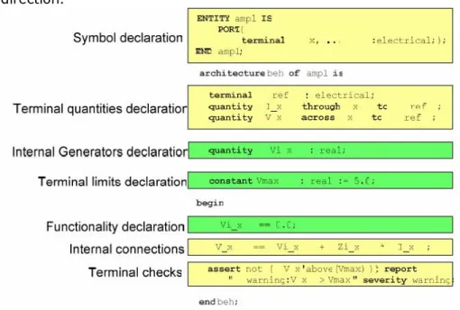
A VHDL-AMS model consists of an entity and one or more architectures. The entity specifies the interface of the model to the outside world. It includes the description of the ports of the model (the points that can be connected to other models) and the definition of its generic parameters. The architecture contains the implementation of the model.
The model template, generated by the create_model.csh script can be customized by the designer to represent the desired behaviour of the full custom analog cell. To help the designer in the customisation of the model the template is divided into different sections and only few of them have to be modified to make the model reflects the desired behaviour of the original transistor-level block.
A preliminary section regards the Library declaration and it is common for all the VHDL-AMS models and includes the IEEE libraries for the electrical system package and some others common libraries for mathematical operations.
In Figure 3-4 generic model template architecture is depicted, the sections to be modified by the designer (specifying internal parameters and functionalities) are highlighted.
The first section includes the entity and the pin-out declaration: the analog pins are declared as electrical terminals and the digital
pins are declared as std_logic specifying the input or output direction.
Figure 3-4: Generic template architecture.
In the second section the branch quantities are defined, they represent the unknowns in the equations describing conservative systems [64][68]. The description of conservative systems can be made graphbased conceptual model. Consider, for example, the bipolar inverter circuit and its equivalent graph, shown in Figure 3-5. The vertices of the graph represent equi-potential nodes in the circuit, and the edges represent branches of the circuit through which current flows. We can divide the branch quantities in:
• across quantities (voltage between two different electrical terminals). They correspond to the potential difference between two vertices in the graph
• through quantities (current flowing through two electrical terminals). They correspond to the edges in the graph
Figure 3-5: Example of across and through quantities.
For any electrical terminal “<terminal_name>” the branch quantities are defined as depicted in Figure 3-6:
• I_<terminal_name>: current through the terminal.
• V_<terminal_name>: voltage across terminal and cell
reference terminal.
The third section regards the internal generators declaration; this section can be modified by the designer in order to use internal quantities for equations definition.
The fourth section regards the Terminal limits declaration and it allows the designer to specify voltage and current limits for every terminal of the cell. These Terminal limits are used during the simulation to check that values of the terminal never exceed the specified ones. If an over range or an under range value occurs a warning message is issued. This automatic check can identify critical situations during simulation and even very dangerous top assembly bugs as like shorts or unconnected power-wires not easy to be discovered with the traditional visual inspection of the analog waveforms, especially for a design with thousands of wires just for the top level interconnections of analog macro blocks.
In the Functionality declaration section, values for internal voltage generators (Vi<x> in Figure 3-6) and impedances (impedance Zi<x> between terminal x and the reference terminal in Figure 3-6) can be specified. The script completes this section with default parameters. The designers can customize the values obtaining the desired behaviour for assuring match with the full custom analog cell.
The sections that regards internal connections contains the constitutive electrical equations of the model. The equations are defined (3-1):
name
term
I
name
term
Z
name
term
V
_
_
=
_
_
×
_
_
(3-1)
Figure 3-6: Terminal check
The last section includes the check definition for performing the over range and under range checks both for voltage terminals and for current terminals. These checks are performed using the VHDL construct assert and the VHDL-AMS function above as in the following example:
assert not (V_term_name’above(Vmax)) report “Warning: V_term_name > Vmax” severity warning;
When the across quantity V<x> values exceeds the voltage limit value V<x>_max decided by the designer the warning message “V<x> > V<x>_max” is issued.
iii. Model cross check
The consistency of the model can be cross-validated with the original analog design, adopting the same test-bench used to validate the transistor-level block and substituting the original cell
<X>
I <X>
Vi<X>
Zi<X>
V<X>
ref
<X>
I <X>
Vi<X>
Zi<X>
V<X>
ref
with the model. Another check can be performed creating a VHDL-AMS smart test-bench that generates the stimuli and performs a self-check test comparing analog outputs of the real cell with those of its behavioural model.
This cross check process increases mixed-signal simulations reliability assuring maximum coherency between the real full custom cell and the behavioural model.
For complex models of big analog cells which are characterised by an elevated number of pins a VHDL-AMS self-checking test-bench can be created. In Figure 3-7 an example of self checking test-bench is proposed: a 16bit DAC. In this example the VHDL-AMS test-bench generates stimuli for both real analog cell and for the model. Output signals are sampled after transistor settling time and a warning is issued if the data related to the model and to the real DAC differ more than 1 LSB.
Figure 3-7: Self-checking Test Bench
3.4. Netlist Automatic Extraction
When all VHDL-AMS models have been developed and the reliability of each model with respect to the original analog cell is guaranteed, the models have to be interconnected coherently with the actual top netlist. To reduce the possibility of mismatch with the real netlist, a CSHell script has been created to obtain an
automatic netlist extraction in order to achieve that all
interconnections between the models in the verilog netlist are perfectly in line with those of the original analog schematic.
The netlist is automatically extracted by the execution of create_nets.csh script. The script recursively goes trough the
analog hierarchy, and by means of the Cadence™ “AMSdirect” engine [71] generates a verilog netlist matching the analog full custom cells structure.
TOP LEVEL
s
w
Mw
Ms
w
Mw
M net WARNING: tree leaf without schematicw
Ms
s
net net INFO: functional view reached ERROR: schematic leaf without model netw
Ms
net Schematic root Schematic leaf VHD-AMS model Verilog wrapperFigure 3-8: Netlist Extraction Flow
In the Figure 3-8 an example of the netlisting flow is provided. The create_nets.csh script starts from the top level of the analog schematic netlist and goes trough the hierarchy, when a correct leaf is discovered the scripts accounts the net, issues an INFO statement that a correct leaf has been detected and continues scanning the hierarchy. A leaf is correct when both Verilog wrapper and VHDL-AMS behavioural model is available and linked to the schematic of the leaf analog cell.
In case the scripts reaches a node in which the Verilog wrapper and the VHDL-AMS models are available but there is no schematic associated to the node a “WARNING” message is arisen to state that we have detected a node with a functional view but without the corresponding schematic.
In case the script identifies any leaf which lacks the model or the wrapper an “ERROR” message is issued and the missing leaf and the library are reported: thus easing the debug phase for a quick fixing of the missing functional view or missing model of the cell. When the scripts is executed with no “ERROR” nor “WARNING” message the AMS compiler can handle instantiated nets, models and wrappers and automatically can perform the compilation. The create_nets.csh script generates indeed a series of log files which can be addressed by the AMS compiler: the Verilog netlist of all hierarchical levels (up to those containing only VHDL-AMS models); a file with the list of all extracted nets; a file containing the list of all the VHDL-AMS models to be compiled; and eventually a file which can provide the data about the list of all the Verilog wrappers to be compiled.
3.5. Connection Modules
To perform a mixed signal simulation of the whole system connection modules, which are able to convert analog signals in logic value and vice versa, are needed. These connection elements are in Verilog-AMS language. The choice of Verilog-AMS instead of VHDL-AMS language to develop the connection modules lays in the in fact that Verilog-AMS features automatic insertion of connect elements during the design elaboration phase thus allowing the designer to gain more flexibility [72]. So the designer just specifies the rules defining the target connect modules for the possible cases of inter-connection (Analog-to-Digital or Digital-to-Analog) in a simple connect_rules file (e.g. see Figure 3-9). On the other hand VHDL-AMS language features no built-in connect rules insertion but requires manual or netlister based insertion of these connection elements.
connect_rules ConnRules_5V;
connect logic_to_elect;
connect elect_to_logic ;
endconnect_rules
The connection modules insertion rules determines how connect element get inserted during design elaboration. In case of conversion from Digital to Analog, the connection element detects the state of the digital drivers at the input of the connection element and provides as output the correspondent analog voltage (see Figure 3-10)
connect_module logic_to_elect(cm,el);
input cm;
output el;
logic cm;
electrical el;
analog begin
V(el) <+ transition((cm == 1) ? 5.0 : 0.0);
endmodule
Figure 3-10: Logical to Electrical Connection Module.
connect_module elect_to_logic(cm,el);
input cm;
output el;
logic cm;
electrical el;
reg kout;
analog begin
always @( above( V(el)-2.5) ) kout=1’b1;
always @( above( 2.5-V(el)) ) kout=1’b0;
assign cm = kout;
endmodule
Figure 3-11: Electrical to Logical Connection Module.
On the other hand, In case of conversion between analog to digital the connection element evaluates the analog voltage at the input, detects the range of the signal and provides the correspondent digital state as output (see Figure 3-11).
3.6. Complete System Simulation
The presented VHDL-AMS verification flow has been used to model and to validate the mixed signal platform interfaces ISIF (see chapter 2) developed in collaboration with SensorDynamics AG and the University of Pisa and a smart platform for resistive sensor interfacing developed in collaboration with SensorDynamics AG (see chapter 5 for more detailed description).
Regarding ISIF verification, thanks to the VHDL-AMS verification flow a huge number of model roughly 100 different models, have been developed in approximately four-man weeks adopting the semi-automatic model generation procedure. Furthermore the flow allowed designers to perform comprehensive simulation of the system as a whole detecting top assembly bugs which are usually very difficult to be discovered with traditional bottom-up validation flows.
The ISIF platform is indeed a complex mixed signal IC with an analog section with a huge number of system configuration switches and the monitoring of all combined effects are very hard to be exhaustively checked by visual inspection.
The ISIF analog section thanks to a programmable approach handled by JTAG-like serial chain is provided with hundreds of bits, used to configure filters, amplifiers, level shifter, input switch matrix and converters which feature a huge variety of configurations difficult to be exhaustively checked with a traditional approach to discover if some state can be dangerous for the platform integrity.
The proposed verification flow allowed designers to identify potential problematic bugs that could not have been discovered without a complete system simulation: swapped bus interface between the analog and digitals DAC drivers, and a control signal pattern (out of the hundreds present) which would have caused a short at the system start-up.
Furthermore the semi-automatic flow approach has appeared to be mandatory since the mixed-signal SoC (for which this behavioural verification has been adopted) has several models, each one with a long list of connections, and it is extremely risky and time-consuming to create manually all the models for such complex system. VHDL-AMS modelling has also featured reducing simulation time: with the presented flow it has been possible to speeds up the simulation by a factor up to three thousands times faster than SPICE simulation: actually 1 msec of complete chip simulation can be simulated in only two hours thus making feasible for designers to simulate system procedures start-up procedure,
boot load execution, and even operating condition with the system connected to a target sensor which has been modelled in VHDL-AMS too. This methodology has allowed designers to achieve first silicon success.
3.7. Critical issues in testing and verification of
mixed signal ICs
In the last years the complexity of mixed-signal ICs has dramatically increased, especially thanks to advances in process technology. Meanwhile, tighter time-to-market requirements have forced companies to reduce the whole product cycle and to review the manufacturing flow to maintain a high level of product quality. The improvements of EDA tools have lead to a conspicuous time speed up for circuit modelling and design.
On the other hand the productivity is still limited by testing which is close to become the most expensive factor for IC companies. The new generation of ICs embed an increasing number of functionalities and configurations which feature complex and flexible architectures for signal conditioning but require new tests, both for analog and digital parts, for significant fault coverage and block characterization, while time-to-market issues are demanding a shorter test time.
While in the digital domain a series of approaches are well established and allow the designers to perform fast and effective test sessions on the new devices, the test of the analog session still lacks of an acknowledged test strategy due to the various difficulties related to analog cells such as non-linearities, parasitics, tolerances and the high complexity of the cells, thus the test of the analog section of a generic mixed-signal ICs has become the main factor of cost for IC companies.
The interest of the academic and industrial research has started focusing on applying structural approaches and extending Design for Testability (DFT) and Built-In-Self-Test (BIST) strategy in the analog domain. In literature we can find several examples of structural approaches [73] [74] [75] [76] and in [77] a methodology for specification-based automated analog test generation and fault simulation is presented. In [78][79] a design method based on IDD monitoring for the detection of parametric and catastrophic faults is described. Possible solutions have been proposed based on two supply current measurements for two “opposite polarity” input signals, and processing the results so that the bias current component is effectively cancelled. [80].
In [81] [82] authors adopt analog test wrappers joined with Test Access Machine (TAM), to simplify test access and unify the test approach for digital and analog blocks, featuring overall testing time reduction.
However these solutions are not tended in the direction of bridging the gap between the design domain and the test domain: the missing connection between design EDA tools and test tools does not allow ICs industries to follow an integrated design to production flow with test-benches unification across all domains from design to test validation, and to compare measurements with data related to design simulations [83].
3.8. Integrated verification flow: from
pre-silicon to post-pre-silicon.
An integrated verification flow has been implemented to bridge the existing gap from pre-silicon simulation to post-silicon verification environments. This verification flow features automating data exchange between design and test environments, with multiple benefits in terms of time, cost, safety and quality of prototyping evaluation. Test is a key issue in a typical product development cycle. At the initial stages of the design, in the pre-silicon phase, simulations are performed to guarantee a correct matching between system specification and simulation results. When the first silicon is back from the foundry (post-silicon phase) the preliminary tests are performed on the prototype for system evaluation and to verify the matching between simulation data and physical measurements.
Thus the key issues that the proposed verification flow is tended to achieve are:
•
Reproduction in prototype evaluation environment ofthe test-bench used during simulation with a twofold benefit of guaranteeing coherency between simulation and verification and to dramatically reduce
the time spent to build up the test environment
.
•
Automatic data comparison from simulation and testtool
.
•
Adoption of a Design For Testability approach inTo meet these requirements and to bridge the gap from design to test domain, an integrated flow to link the pre-silicon simulation
environments and the post-silicon verification has been created
.
3.9. Integrated verification flow: simulation
environment.
In order to achieve an integrated environment which allows designers to perform automatic import and data comparison between simulation and test, a tool for analyzing the system at design level as a whole is required (since in laboratory complete tests of the entire system are performed extracting and elaborating data that can be both analog and digital).
In order to perform simulations of the whole system the adoption of a hardware description language oriented to mixed signal design is mandatory. We have chosen the VHDL-AMS [64] [65] [66] [67] [84], (see section 3.2) since it features a quick and effective modelling of analog, digital and mixed-signal blocks and allow designers to achieve full system simulation.
Furthermore a comprehensive set of libraries have been developed in VHDL-AMS language for setting up a simulation environment which can be completely overlapped with test environment. Thus a set of VHDL-AMS cells allow generation of stimuli to be executed as in laboratory with a generic waveform generator for signal generation. VHDL-AMS procedures has been developed for data monitoring, extraction and elaboration as it can be performed in laboratory with a multimeter for signal acquisition and a PC for data elaboration.
3.10. Integrated verification flow: verification
environment.
To recreate the environment adopted at simulation level with VHDL-AMS on the verification and validation of the prototype in laboratory a proper test programming language has to be adopted. Furthermore the test programming language has to handle a various sets of measurements that have to be performed in the lab to evaluate the real performance of the system under test and for fault detection. In literature we can find several examples of the use of programming languages (C, Visual Basic, LabWindows or LabVIEW) for test procedures automation.
National Instruments LabVIEW [85] [86] [87] provides the flexibility of a programming language and features a wide series of built-in tools designed specifically for test, measurement, and control. Furthermore Test equipment industries, being National Instruments LabVIEW an acknowledged test programming language [85] [86] [87], has started providing the measurement set-up instrumentation for laboratory with native drivers in LabVIEW language for an easy instrumentation interfacing: thus designers can embed measurement devices directly in the test program simply linking the pre-built LabVIEW interface.
LabVIEW features also a specific native target for helping designers to rapidly built interactive graphical user interface in order to handle the test routine with a friendly and interactive interface.
We have developed a LabVIEW wrapper of the whole system which allows direct system handling and programming, the wrapper can accept an input file for system configuration in which all the settings for the configuration of the system under test and the signal generation and acquisition are defined. This input file can be ported directly from simulation environment to verification domain with a twofold benefit: (i) reduction of time needed to re-design test configuration; (ii) assurance that the desired simulation test will be exactly replicated on the physical prototype with exact alignment between simulation and verification thus making output data perfectly coherent.
We have developed a generic graphical user interface (LVGUI) which displays and renders clearly the configuration parameters of the system allowing the designer to perform a rapid check of the whole system at first glance. The LVGUI is indeed an effective tool not only for system programming but also for particular system setting investigation. This feature is extremely powerful in the first evaluation stage when the prototype is in the bring-up phase, since in this phase a high degree of interactivity is required to investigate possible problems.
Thanks to the enhanced interactivity of the LVGUI unexpected behaviours with respect to simulation due to unforeseen and undesired conditions, can be studied, investigated and moreover the LabVIEW model permits a formalization of the critical conditions that revealed a possible particular behaviour to be performed. Therefore in case the prototype will probably not be the last, the LabVIEW model allows designers to easily recreate on simulation side critical conditions during the re-design of the system reducing the time spent in iterating trough the design process.
3.11. Integrated verification flow: Design For
Testability approach.
A fundamental aspect of this approach is based on the possibility to have a high degree of observability and controllability of the system under analysis: a Design For Testability approach (DFT) is therefore needed and proper basic structures are required to make the integrated flow effective.
Moreover a DFT approach is mandatory in all application fields which necessity strict requirements of safety or highly reliability (e.g. for the life-science, the nuclear energy generation, or the transportation industries including automotive, and aerospace applications), in fact high testability and functional verification can guarantee a safe and reliable operation. Furthermore, legislative requirements and demands from insurers in many cases necessitate proof on “completeness” in testing after manufacture and even on-line verification capabilities for certain applications. An important issue on improving testability is the accessibility of nodes. Submicron technologies has lead to an high level of integration lodging millions of transistors into a single chip, and consequently making each point of interest reachable has become a critical point. Techniques on signals injection into embedded modules/nodes (controllability) and on response access the (observability) with adequate resolution are essential for this purpose [88]. In digital system, access to single points of the circuits is guaranteed by the widely diffused scan-path approach [89] [90]; while in mixed signal circuits it is handled by an analogue test bus used in combination with CMOS switches [91] [92]. During the test phase, the nodes of interest can be connected to the chip output on two dedicated pins by the analog bus through which stimuli can be brought in or signals can be lead out of the asic.
Another key point of the proposed approach is the use of a processing unit since it allows a dedicated firmware (FW) for setting system parameters to be handled. Furthermore the presence of a CPU allows high level of complexity test to be performed and an efficient handling for built in tests with internal waveform generation and signal detection. In the last few years, recent advances in the semiconductors technology has lead towards integrated circuits that embed millions of transistor on a single chip making the use of a CPU no more an excessive requirement.
3.12. Integrated verification flow: overall flow
implementation.
During system simulation an evaluation firmware is developed in order to perform complete evaluation of the system using VHDL-AMS model of the whole asic activity (start-up, power down condition, boot-load) in mixed simulations. Moreover in the prototyping phase the same FW can be partially reused for debug, characterization and trimming purpose.
The proposed approach basically consists in enhancing the FW by adding, as comments, the information related to testing set-up. This additional information can be extracted both during test and design phases to determine how to set input stimuli: thus the same test-benches are easily replicated in both the environments and the acquisition of coherent output data can be guaranteed. The FW itself represents the actual link which features bridging the gap between design and test environment linking pre-silicon simulation to the physical test world. At simulation level is indeed handled by VHDL-AMS simulation environment with the whole system module and in prototyping phase the FW is downloaded directly inside the real device.
In Figure 3-12 the overall flow is depicted. A VDL-AMS model of the whole system by means of a semi-automatic flow [93] [94] has been created in the design phase (see section 3.3) and a library of VHDL-AMS routines have been created for signal generation and data acquisition and elaboration. Thus a module for reproducing generic waveform generator is connected to the input analog test bus, while a series of scripts elaborate the instruction contained in the FW for configuring properly this module, setting its internal parameters. Other modules are configured for appropriate data acquisition connected to the output test bus. A simulation report in text format is eventually generated after data elaboration.
National instrument LabVIEW has allowed us to re-create the same environment used in simulation in test phase. An input LabVIEW routine extracts information from the FW and set a generic waveform generators which can refer to a real waveform generator present in laboratory or to on chip signal production.
A further module performs data extraction and elaboration, with a final test report generation in text format compliant with the simulation one. At the end of the process a final LabVIEW module compares the two reports from simulation and from test system performance, matching and highlighting main data report discrepancies for a quick review and debug.
Figure 3-12: Integrated Verification Flow
To guarantee a high degree of interactivity a LabVIEW visual interface has been developed. This interface (LVGUI) allows designers to get a clear and complete view of the system configuration at first glance; in addition the designer can also modify desired parameters of the FW downloaded in the prototype creating a new one and saving configuration set-up for back annotation in simulation environment. The customization of the test structure can be extremely rapid, thus creating a new system configuration or even a new approach for signal management with an automatic FW generation ready to be downloaded in the chip under test or to be re-used at simulation level. The LVGUI interface concurs significantly in performing a rapid and comprehensive system debug and investigation. Particular
behaviours and unforeseen phenomena arisen during test can be rapidly formalized and measurements defined in lab can be easily transferred to validation and simulation thanks to the proposed integrated environment.
3.13. Validation of the verification flow
The proposed integrated verification flow has been validated on a complex mixed signal ICs for interfacing a wide class of sensors: ISIF (Intelligent Sensor InterFace) developed in collaboration with SensorDynamics AG (see chapter 2) is a mixed-signal chip conceived to speed up a Platform Based Design Flow, which significantly reduces the time needed for design space exploration and system architecture validation. It features a wide set of analog and digital IPs, with highly programmable interconnections, in order to implement a DSP chain to be straight prototyped with the target sensor, thus avoiding long and potentially inaccurate system simulations. As case of study the application of the verification flow on 12 bit DAC integrated in a platform is reported in this section
(
see Figure 3-13).Figure 3-13: ISIF Block Diagram
For an effective monitoring of the cells and the internal signals, an input/output test bus can be driven to supply external stimuli or to probe output signals at each block end, guaranteeing an effective and quick way to debug the analog signal conditioning path
guaranteeing a high level of observability. To increase the controllability, that is a key point of the previously described verification flow, in the digital section of our test case a set of registers, connected to the Advanced Microprocessor Bus Architecture (AMBA) bus, have been used to check the internal functionalities of the digital section. Analog test buses and registers are programmable trough a JTAG-like approach for handling the digital bits used for analog block configurations, thus overcoming clock skew issues and allowing safe communication between digital and analog world.
The ISIF platform features high resolution ADC and DAC converter: hence signal generation and acquisition can be performed directly on-chip. Analog signals can be converted and afterwards processed in digital domain thanks to the powerful CPU based on the LEON core and to the flexible hardware DSP structure oriented to the complex processing required for signals conditioning and elaboration. The generated signal can be also directly directed outside the asic through four dedicated pins for external elaboration.
To guarantee a safe configuration of the platform, even when the settings are changed interactively, a dedicated LabVIEW Graphic User Interface (LVGUI) has been developed (see Figure 3-14). Since for each IP the JTAG-like configuration is composed of hundreds of bits a manual approach can not guarantee reliability and a guided approach is mandatory.
This interface can download the firmware directly on chip through the UART thus featuring platform configuration (the FW contains the JTAG-like chain and registers settings) and even performing through an enhanced firmware prototype evaluation. The LVGUI can also perform read back of JTAG-like chain, displaying register contents and expressing also their physical implication.
During physical test on the prototype particular behaviours, unexpected from simulation analysis, may arise; in this case, the engineer can modify, through the LVGUI, the system configuration and test settings to examine the event and detect properly reasons that caused unforeseen performances. These settings and the performed investigations can be saved in a text file and furthermore formalized to be imported in the simulation environment: in this manner we can guarantee to recreate at pre-silicon level the condition for the unforeseen phenomena.
Figure 3-14: LabVIEW Graphic User Interface
As case of study the application of the verification flow on 12 bit DAC to drive an external generic sensor integrated in the ISIF platform is described.
Since first stage of DAC design, designers have performed the validation of this IP trough test-benches oriented to highlight offset error, gain error, differential nonlinearity (DNL), and integral nonlinearity (INL), thus focussing on parameters which represent the most important specifications for a digital to analog converter For evaluating these parameters proper stimuli have to be applied to the cell under test: for example the DAC have to be driven by a digital ramp wave: consequently the digital section has to provide through a JTAG-like controller, DAC stimuli and also surrounding settings for cells correct configuration: voltage references to DAC, analog bus enabling, power-down disabling and others configuration bits resulting in a high number of digital registers to be set correctly to generate the desired ramp.
In a standard test approach the set-up of the complete test procedure could have required a great amount of time with a consequent high scene of configuration errors. With the proposed approach in the design phase a proper firmware has been already developed in order to evaluate at simulation level the performances of the IP under test. Furthermore the firmware, can embed a series of information (set as comments) to describe the
signal generation and acquisition strategy. With the LVGUI the FW, previously developed at design level, is automatically downloaded into the asic and allows the set-up of the instrumentation to be automatically performed. Firmware is parsed from LVGUI that recognizes that a DAC is under test, so that the multimeter (in our application we used Agilent 34401A) is automatically programmed through GPIB interface to evaluate DAC output DC voltage. The LabVIEW sub-routine can handle a wide series of lab instrumentation configuring each time the selected one according to the information extracted by the FW. Furthermore the LabVIEW library can handle multiple typologies of the same instrumentation, since in these last few years all the measurements company provide their instrumentation with built-in native low level driver for a plug & play interfacing of the new measurement unit in the test program.
The multimeter data evaluations are then sent back to the LVGUI interface which performs, through dedicated sub-routines, data elaboration and displays the results. Moreover a test report is produced containing the measurement data and the previous mentioned specifications (DNL, INL, offset).
Then another specific LabVIEW modules process this report comparing the measured results with the expected ones contained in the simulation report produced at design level by a VHDL-AMS module during the simulation of the cell under test. The VHDL-AMS module is partially showed in the following Figure 3-15 for the presented case study.
In Figure 3-16 we can observe a portion of the measured transfer function of DAC versus the simulated one and in Figure 3-17 the difference between them is reported. In the following Tab the main differences between measurements and simulations data contained in the final report, are highlighted. .
DNL MAX DNL MIN INL MAX
TEST 2.432mV 23µV 4.788mV
SIMULATION 2.665mV 24µV 5.025mV
DEVIATION 9.58% 4.30% 4.94%
Table 4: Performance comparison between simulation and measurements
if (clk’event and clk='1') then --dac output voltage sampled v_dac_sampled <= v_dac; --on positive edge of clk
v_dac_inl <= abs (v_idac–v_dac); --INL calculation v_dac_lsb <= v_dac_sampled-v_dac_sampled_old; --DNL calculation
end if;
. . .
if (v_dac_inl > inl_max) then inl_max <= v_dac_inl; --INL max value updating
if (v_dac_inl < inl_min) then inl_min <= v_dac_inl; --INL min value updating
if (v_dac_lsb > dnl_max) then dnl_max <= v_dac_lsb; --INL max value updating
if (v_dac_lsb < dnl_min) then dnl_min <= v_dac_lsb; --INL max value updating
. .
. .
write_report : process (…)
FILE outFile : TEXT open WRITE_MODE is “dac12_doc.txt”; VARIABLE outLine : LINE;
begin write (outLine,”inl_max:”); write (outLine,inl_max); write (outLine,HT); write (outLine,”inl_min:”); write (outLine,inl_min); write (outLine,HT); write (outLine,”dnl_max:”); write (outLine,dnl_max); write (outLine,HT); write (outLine,”dnl_min:”); write (outLine,dnl_min); write (outLine,HT); writeline (outFile,outLine);
end process write_report;
Figure 3-15: Partial content of VHDL-AMS module generating the report
Figure 3-17: Difference between simulated DAC transfer curve and real curve.
The development of the described environment comprehensive of the dedicated LVGUI consisted of about 8 weeks/man to be added to a traditional design flow starting from scratch. With minor modifications, quoted in terms of 2-3 weeks/man, the environment can be re-built for a generic asic which respond to the minimum requirements of controllability and observability and which embeds a CPU.
Bibliography
[58] ‘Ken Kundert, Henry Chang, Dan Jefferies, Gilles Lamant, Enrico Malavasi, Fred Sendig: Design of Mixed-Signal Systems on Chip. IEEE Transactions on Computer-Aided Design of Integrated Circuits and Systems, vol. 19, no. 12, pp. 1561-1571, December 2000.
[59] L.Fanucci, F.Iozzi, C.Marino, A.Giambastiani, A.Rocchi: Platform Based Design for Automotive Sensor Conditioning. Proceedings of Design, Automation and Test in Europe, 2005. Page(s):186 - 191 Vol. 3
[60] L.Fanucci, F.Iozzi, C.Marino, A.Giambastiani, A.Rocchi: Mixed Signal Platform Based Design for Automotive Sensor Interface. Eurosensors 2004. Sept. 2004 Rome.
[61] Walden C. Rhines: Discontinuities in Analog, Mixed Signal Design. Electronic News, 6/4/2001.
[62] Gabe Moretti: Find and Fix Problems Early in the Design Cicle. TechTrends, www.edn.com , Oct. 30, 2003.
[63] Georges G. E. Gielen, Rob A. Rutenbar: Computer-Aided Design of Analog and Mixed-Signal Integrated Circuits. Proceedings of the IEEE, Vol. 88, No. 12, Dec 2000.
[64] Ernst Christen, Kenneth Bakalar: VHDL-AMS A Hardware Description Language for Analog and Mixed-Signal Applications. IEEE Transactions on Circuits and Systems-II: Analog and Digital Signal Processing, Vol. 46, No. 10, Oct. 1999.
[65] Francois Pecheux, Christophe Lallement, Alain Vachoux: VHDL-AMS and Verilog-VHDL-AMS as alternative Hardware Description Languages for Efficient Modeling of Multidiscipline Systems. IEEE Transactions on Computer-Aided Design of Integrated Circuits and Systems, Vol. 24, No.2, Feb. 2005.
[66] IEEE Computer Society: IEEE Standard VHDL Analog and
Mixed-Signal Extensions, IEEE Std 1076.1-1999. Design Automation Standards Committee of the IEEE Computer Society, March 18, 1999.
[67] Peter J Ashenden, Gregory D. Peterson and Darrell A. Teegarden: The System Designer's Guide to VHDL-AMS. Morgan Kaufmann Publishers Sept. 2002.
[68] K. S. Kundert, O. Zinke: The Designer's Guide to Verilog-AMS. Kluwer Academic Publisher, 2004.
[69] Ayman Mounir, Ahmed Mostafa, Maged Fikry: Automatic Behavioural Model Calibration for Efficient PLL System Verification. DATE 2003 Designers' Forum.
[70] Cadence™ Virtuoso Analog Design Environment, User Guide, Product Version 5.0.33.
[71] Cadence™ Virtuoso AMS Environment, User Guide, Product Version 5.0.33.
[72] Olaf Zinke: Bi-directional Mixed Signal Connection modules for automatic insertion.
[73] Cheng-Wen Wu: SOC Testing Methodology and Practice. Proceedings of the Design, Automation and Test in Europe Conference and Exhibition (DATE’05).
[74] L. S. Milor: A Tutorial Introduction to Research on Analog and Mixed-Signal Circuit Testing. IEEE Transactions on Circuits and Systems-II: Analog and Digital Signal Processing, Vol.45, No.10, Oct. 1998.
[75] V. D. Agrawal: Testing in a mixed-signal world. Proc. IEEE ASIC Conference and Exhibit, pp. 241–244, 1996.
[76] A. Chatterjee, N. Nagi: Design for testability and built-in self-test of mixed-signal circuits: a tutorial. Tenth International Conference on VLSI Design, 1997. Proceedings pages:209 - 214, July 1997 [77] S. Ozev, A. Orailoglu: An integrated tool for analog test
generation and fault simulation. Quality Electronic Design, 2002 Pages: 267-272.
[78] W. M. Lindermeir, T. J. Vogels, H. E. Graeb: Analog test design with IDD measurements for the detection of parametric and catastrophic faults. DATE98 Pages: 822-827.
[79] Soden, J.M. et al, IDDQ Testing : A Review, Journal of Electronic Testing : Theory and Applications, 3, 1992 pp291-303.
[80] Andrew Richardson1, Adrian Bratt1, Iluminada Baturone2 & Jose
Luis Huertas2 “The Application of IDDX Test Strategies in Analogue and
Mixed Signal IC’s. IEEE Mixed Signal Test Workshop, Grenoble, 20th-22nd June 1995.
[81] A. Sehgal, S. Ozev, K. Chakrabarty: TAM optimization for mixed-signal SOCs using analog test wrappers. ICCAD-2003. Pages: 95-99.
[82] A. Sehgal, F. Liu, S. Ozev, K. Chakrabarty: Test planning for mixed-signal SOCs with wrapped analog cores. DATE05. Pages:50-55 Vol.1
[83] T. Austin, C. Canlas, B. Morgan, J. L. Rodriguez: Across the great divide: examination of simulation data with actual silicon waveforms improves device characterization and production test development. Test 2002 Pages:270-279.
[84] IEEE Computer Society: IEEE Standard VHDL Analog and
Mixed-Signal Extensions. IEEE Std 1076.1-1999. Design Automation Standards Committee of the IEEE Computer Society, 1999.
[85] http://www.ni.com/labview.
[86] “LabVIEW: Getting Started with LabVIEW”, National Instruments User Manual, Aug. 2005.
[87] Gary W. Johnson, Richard Jennings: LabVIEW Graphical Programming. McGraw-Hill Professional, July. 2001.
[88] Andrew Richardson, Thomas Olbrich, Valentino Liberali, Franco Maloberti “Design for test strategies for analog and mixed signal integrated circuits”
[89] K. Parker: The Boundary-Scan Handbook. Kluwer Academic Publischers, Massachussets, 1992.
[90] M.Abramovici, M.A.Breuer, and A.D.Friedman, Digital System Testing and Testable Design, New York: Computer Science Press, 1990.
[91] Gordon W. Roberts: Improving The Testability Of Mixed-Signal Integrated Circuits. IEEE Custom Integrated Circuit Conference 1997. Pages: 214-22.
[92] S. K. Sunter: Cost/benefit analysis of the P1149.4 mixed-signal test bus. IEE Proc.-Circuits Devices Syst., Vol. 143, No. 6, Dec. 1996.
[93] C. Marino, M. Forliti, A. Rocchi, A. Giambastiani, F. Iozzi, M. De Marinis, L. Fanucci: Mixed signal behavioural verification using vhdl-ams. 2005 PhD Research in Microelectronics and Electronics, Pages: 315-318 Vol. 2.
[94] C. Marino, M. Forliti, A. Rocchi, F. Iozzi, A. Giambastiani: VHDL-AMS Modelling and System Verification Flow for Mixed-Signal System-On-Chip. FDL05 Forum on specification & Design Languages Sept. 27-30 Lausanne.