When I was a child, I read of fairy tales in which mystical creatures and beautiful fairies swept their wand in the air, creating beautiful trails of light and fairy dust made of gold. During my PhD, I discovered that if you sweep a laser inside of a metal precursor you can create
gold nanoparticles in the trajectory and build structures made of gold. I don’t believe in fairy tales anymore, but I believe in science and it’s just as magic.
Abbreviations iii
Abstract v
Abstract (Italian) viii
Introduction 001
Contents 011
1 Micro- and Nano-fabrication through single and multiple photons absorption 016
1.1 Single photon photolithography 016
1.2 Two-photons absorption (TPA) 020
1.3 Two-photons polymerization (TPP) 022
1.4 Two-photons Direct Laser Writing (TP-DLW) 024
1.4.1 Modelling 025
1.4.2 Analysis 026
1.4.3 Voxel characterization 028
1.5 Meso-scale structures 032
1.5.1 Shell & Scaffolds 033
1.5.2 Developing issues 033
1.6 Conclusions 035
2 Micro-fabrication of 3D structures in Reactive Mesogens 036
2.1 Liquid Crystals 036
2.1.1 Nematic Liquid Crystals (NLCs) 037
2.1.2 Chiral Liquid Crystals (CLCs) 042
2.2 Microfabrication in Liquid Crystalline Polymer 046
2.2.1 Birefringence analysis 051
2.2.2 TP-DLW effects on birefringence 056
2.2.3 Photoluminescence in RMs 3D structures doped with dyes 062
2.3.2 TP-DLW effects on chiral RMs 069
3 Optical control of metal nanoparticles created by photo-reduction of metal precursors
through TP-DLW 079
3.1 Two-photon photo-reduction (TPPR) of metal precursors in polymeric matrix 079 3.2 Voxel characterization of two-photon photo-reduced gold nanoparticles (GNPs)
082 3.3 Density and poly-dispersity analysis on the GNPs created during TP-DLW
087
3.4 Diffusive and thermal effects overview 090
3.4.1 Diffusive effects 091
3.4.2 Water diffusion 095
3.4.3 Blast effects in water solutions. 108
3.4.4 Thermal effects 112
3.5 Control of the ions diffusion through electric fields 120 4 TP-DLW of gold nanoparticles for thermo-plasmonics and detecting applications 129 4.1 Localized surface plasmon resonance (LSPR) 130 4.2 SERS enhancement scattering from TP-photo-reduced arrays of GNPs 132
4.3 Thermo-Plasmonics 136
4.3.1 Photo-thermal effects on randomly distributed gold nanoparticles 137 4.3.2 Photo-thermal effects on 1D gratings of gold nanoparticles 143
Acknowledgments 149
Conclusions 150
List of Figures 156
1D One-dimensional
2D Bi-Dimensional
3D Three-Dimensional
AFM Atomic Force Microscope BSEs Back-Scattering Electrons CAD Computer-Aided design CLC Cholesteric Liquid Crystal CRMs Cholesteric Reactive Mesogens
DMOAP Dymethiloctadecyl[3-(trimethoxysilyl)propyl]ammonium chloride DLW Direct Laser Writing
GNPs Gold Nanoparticles
EBL Electron Beam Lithography EDL Electric Double Layer EDX Energy Dispersive X-Ray
EF Enhancement Factor
IPA Isopropyl Alcohol ITO Indium Tin Oxide
LC Liquid Crystal
LCE Liquid Crystalline Elastomer LCP Liquid Crystalline Polymer
LP Laser Power
LSPR Localized Surface Plasmon Resonance NIR Near Infra-Red
NLCs Nematic Liquid Crystals NPs Nanoparticles
PL Photo-luminescence PVA Polyvinyl Alcohol
QR Quick Responsive
RMs Reactive Mesogens SEs Secondary Electrons
SEM Scanning Electron Microscopy SERS Surface-Enhanced Raman Scattering SPA Single Photon Absorption
SS Scan Speed
STL Stereolithography
TP-DLW Two-Photons Direct Laser Writing TPA Two-Photon Absortoption
TPP Two-Photon Polymerization TPPR Two-Photon Photo-Reduction
UV Ultra-Violet
Abstract
In the field of nanotechnologies the Two-Photons Direct Laser Writing (TP-DLW) is the most advanced optical technique for creating arbitrarily complex 3D structures in organic resists, featuring details down to 50 nm, well below the diffraction limit.
More recently, this technique has been used in “resists” containing a photosensitive metallic precursor, activated by the two-photon absorption (TPA) process, allowing for the creation of metallic nanoparticles clusters inside to the focus figure of a highly focused laser beam, where the TPA threshold intensity is reached.
The aim of my PhD work was the elucidation of the physical processes involved in the realization of 3D nanostructures made in different materials for applications in micro-fluidics and advanced optics. In particular, I carried out studies on both isotropic and anisotropic photoresists, and on metallic precursors.
Concerning the isotropic photoresists, I have investigated the capabilities and the limits of the TP-DLW technique, on the fabrication of microfluidic systems and elements of millimetric size, with micro- and nano-features printed inside the channels.
The best results in printing such millimetric structures in terms of geometrical compliance and fabrication time are achieved, by combining the single (SPA) and the two-photon absorption (TPA) processes. The latter one allowed for the creation of a shell, an internal structural scaffold and eventual microscopic details, whereas the former one to polymerize the bulk of the object. However, the development step of microfluidic systems (i.e. the removal of the un-polymerized resist) is quite challenging in general, due to possible swellings and consequent distortions in the structure geometry. In my PhD, I developed an effective protocol to face this issue.
The application of the TP-DLW technique to anisotropic reactive mesogens (RMs) resulted in very interesting achievements, as it allowed for the fabrication of 3D solid
mechanical properties of polymers. Effects of the direct laser writing on the internal molecular order of the reactive mesogens have been thoroughly investigated, to ensure a fine control on the optical properties of 3D objects made in liquid crystalline elastomers. Analyses of the physical processes, which occur during TP-DLW and allow for tuning of the optical response of the printed 3D solid structures are shown. Appropriate doping of the reactive mesogens with dyes and chiral dopant agents were performed to investigate different fields of applications.
In particular, a chiral agent confers helical order to the RMs, which show selective Bragg reflection of the impinging light in both wavelength and polarization. Micro-fabrication of 3D chiral structures is a brand new field that is paving the way to the creation of photonic devices, such as micro-laser of defined shape, white light reflective object, anti-counterfeiting and data storage systems.
I performed a series of experiments aimed at demonstrating the possibility to manipulate the helical structural order of the liquid crystals during TP-DLW. As a consequence, multi-colour three-dimensional structure can be created.
Finally, the possibility to include metallic details in polymeric objects or even to create metallic structures would pave the way for the DLW of metallic/polymeric nano-composites. I performed experiments with polymeric or hydrogel matrices doped with a suitable metallic precursor, in a free surface drop cast, or in cell segregated thin film, onto a glass substrate. In such system, I was able to create 1D gratings made of GNPs stripes with single or multiple laser sweep. I demonstrated that the stripe width increases with the laser power and the exposure time, showing a behaviour similar to the photo-polymerization, as expected. I also analysed the influence of the exposure time over the nano-particles size distribution and density and showed that by suitably adjusting the exposure time it is possible to maximize the occurrence of a given diameter.
The experiments were aimed at elucidating the involved physical phenomena, beyond the bare optical absorption. In particular, the key-role of thermal and diffusive processes have been analysed. TPA leads to the photo-reduction of ions of AuCl4 – and the
a thermal shock-wave is generated and is responsible of the local dehydration in the spot area. Due the concentration gradients of the ions of gold precursor and of water, different diffusive processes take place, occurring on different timescales. Therefore, different characteristic times are observed for the ion and the water diffusion, in the polymeric matrix. My experiments demonstrate that the diffusive effects can be exploited for controlling the NPs density and size when a given energy dose is delivered in multiple shots, by tuning the time interval between each shots. Preliminary experiments on the possibility to control the growth of GNPs through the application of specific electric field during TP-DLW were performed as well.
Last but not least, the possibility to use TP-DLW of metal precursor to realize smart platform rich in GNPs suitable to different application is shown. In particular, I demonstrate that, controlling the pitch and the size of GNPs stripes, it is possible to create both thermo-platform whose thermal response to external light is tuneable, and detecting substrates for Surface-Enhanced Raman Spectroscopy (SERS). The Raman spectra were recorded from samples immersed in a solution of rhodamine-6G (R6G), as well as, after exposure of the samples in xylene. SERS enhancement factors of up to ~104 were obtained for both
Nel campo delle nuove tecnologie, la scrittura laser diretta a due fotoni (dall’inglese two-photon direct laser writing TP-DLW) è la tecnica ottica più avanzata per la creazione di strutture 3D complesse, che presentano dettagli inferiori al limite di diffrazione fino a 50 nm.
Solitamente, la stampa diretta a due fotoni avviene in monomeri organici fotosensibili, noti come photoresist, che possono polimerizzare per assorbimento a uno (single photon absorption, SPA) o due fotoni (two-photon absorption, TPA). Negli ultimi anni, questa tecnica è stata utilizzata anche per ottenere aggregati di nanoparticelle a partire da matrici polimeriche drogate con precursori metallici.
Quando un fascio laser è focalizzato all’interno di un materiale fotosensibile, nella regione del fuoco in cui la soglia di assorbimento a due fotoni è superata, si assiste all’eccitamento delle molecole, le quali possono rilasciare energia (attraverso fluorescenza o calore), o in alternativa legarsi attraverso processi di polimerizzazione (resine organiche) o ridursi (precursori metallici).
Lo scopo del mio dottorato è stato studiare i processi fisici coinvolti nella realizzazione di nano-strutture 3D composte da diversi materiali, per applicazioni in campo della micro-fluidica o dell’ottica avanzata. In particolare, i materiali usati sono stati photoresist organici, sia isotropi che anisotropi, e soluzioni acquose di alcol polivinilico drogate con acido tetracloroaurico.
Nel caso di photoresist isotropi, ho studiato le capacità e i limiti della tecnica TP-DLW, concentrandomi sulla fabbricazione di sistemi micro-fluidici di dimensioni millimetriche, ma con micro- e nano-dettagli presenti all’interno dei canali.
I migliori risultato nel processo di stampa delle suddette strutture millimetriche, in termini di conformità geometrica e tempo di fabbricazione, sono stati ottenuti combinando insieme SPA e TPA. Tramite TPA è stato possibile creare il guscio esterno (shell) della struttura e un’impalcatura interna (scaffold) atta a sorreggerla. Inoltre, tutti i dettagli
invece, è stato polimerizzato attraverso SPA. Tuttavia, il processo di sviluppo di un sistema micro-fluidico (ad es. la rimozione di tutto il photoresist non polimerizzato) può rivelarsi una sfida e portare a deformazioni o conseguenti distorsioni della geometria del sistema. Durante il dottorato, quindi, ho sviluppato un protocollo che permette di sviluppare efficacemente il campione, superando questo ostacolo.
L’uso della TP-DLW in photoresist anisotropi, composti da mesogeni reattivi (reactive mesogens, RMs), ha permesso di ottenere risultati estremamente interessati. In particolare, ho realizzato strutture 3D che mantenessero le proprietà ottiche dei cristalli liquidi usati, pur acquisendo le tipiche proprietà meccaniche dei polimeri.
Al fine di ottenere un controllo fine sulle proprietà ottiche degli oggetti creati, gli effetti della scrittura laser diretta sull’ordine interno dei mesogeni reattivi sono stati analizzati con particolare attenzione. Nel corso del lavoro sono illustrati i risultati ottenuti e i processi fisici che consentono di modulare la risposta ottica di un oggetto creato in RMs, in funzione dei parametri di scrittura. Inoltre, al fine di ampliare i campi di applicazione consentiti dalla TP-DLW di strutture solide di cristallo liquido, ho drogato opportunamente l’RMs con agenti chirali o coloranti fluorescenti.
In particolare, gli agenti chirali hanno la proprietà di conferire ordine elicoidale ai mesogeni reattivi del photoresist, il quale presenterà dunque riflessione selettiva alla Bragg della lunghezza d’onda e della polarizzazione della luce incidente. La micro-fabbricazione di strutture chirali tridimensionali è un campo altamente innovativo che consente la creazione di dispositivi fotonici (ad es. micro-laser di forma arbitraria), micro-strutture in grado di riflettere la luce bianca, o sistemi di anticontraffazione e conservazione di dati.
Gli esperimenti effettuati hanno dimostrato la possibilità di manipolare l’ordine elicoidale del cristallo liquido chirale, durante la TP-DLW. Di conseguenze, sono riuscita a micro-fabbricare strutture multicolorate.
In ultimo, la possibilità di includere nano-particelle metalliche in strutture polimeriche, consentirebbe la realizzazione di oggetti nano-compositi. A questo proposito, ho svolto numerosi esperimenti in matrici metalliche o gel, opportunamente drogati con un
elettrolitiche.
In particolare, ho creato reticoli 1D di nano particelle di oro (gold nanoparticles, GNPs), attraverso una o più passate del fascio laser, dimostrando che la larghezza delle strisce di GNPs ottenuta dipende dalla potenza e dal tempo di esposizione, in maniera analoga a quella prevista nel caso di foto-polimerizzazione. Inoltre, ho analizzato l’influenza del tempo di esposizione sulla taglia delle GNPs create a parità di energia, osservando come il diametro medio delle nano-particelle possa essere modulato.
Ulteriori esperimenti sono stati svolti al fine di chiarire i fenomeni fisici coinvolti durante il processo di TP-DLW, al di là del solo assorbimento ottico. In particolare, ho analizzato il ruolo fondamentale dei processi termici e diffusivi. Per TPA si ha la riduzione dello ione cloroaurico AuCl4 – e la conseguente creazione di GNPs, tuttavia al contempo si
assiste ad un riscaldamento locale del campione. Questo riscaldamento è responsabile della formazione di un’onda d’urto termica e conseguente deidratazione locale. Si vengono così a creare gradienti di ioni cloroaurici e di acqua, che danno luogo a processi diffusivi all’interno della matrice, con diversi tempi caratteristici.
I miei esperimenti hanno mostrato che gli effetti diffusivi possono essere sfruttati per controllare la densità e le dimensioni della nanoparticelle create, frazionando la dose di energia distribuita e variando il tempo di attesa tra una esposizione (shot) e la successiva. Inoltre, qui presento un lavoro preliminare sulla possibilità di controllare la crescita delle nanoparticelle applicando un campo elettrico durante TP-DLW, all’interno di una cella elettrolitica.
In ultimo, ma non meno importante, l’uso della TP-DLW con un precursore metallico consente di creare delle “piattaforme” composte di nanoparticelle d’oro che possono essere usate in numerose applicazioni. In particolare, ho studiato gli effetti termo-plasmonici di reticoli fatti da GNPs, dimostrando come sia possibile modulare la variazione di temperatura in funzione del passo del reticolo. Inoltre, strutture 1D di GNPs possono essere utilizzati come substrati per la spettroscopia Raman amplificata da superfici (Surface-Enhancement Raman Spectroscopy, SERS). Gli spettri Raman sono stati acquisiti immergendo
1
Introduction
In the last decades, micro- and nano-fabrication processes have been of great interest, both in scientific and in technological fields, due to the possibility to fabricate systems and devices featuring micrometer and nanometer resolution [1-3]. Between the different technologies, optical lithography is the most used and investigated ones [4], thanks to the possibility to use light as a tool to micro-structure a photosensitive material.
Due to their flexibility and the possibility to be employed in a wide range of applications, polymers are widely used in micro-fabrication processes [5-8]. Depending on the characteristic of to the selected polymer, ultra-violet (UV) radiation may either break the links between molecules (positive photo-resist), making the irradiated areas soluble in a developing solvent and may then be removed through chemical processes, or generate cross-linking between monomers (negative photo-resist) [9].
In both cases, a mask is usually required to cover the areas that have not to be exposed. Therefore, the structure resolution is determined by the diffraction limit. In recent years, electron-beam lithography (EBL) has been employed to overcome this limit. An electron beam is used to design the structures on a resist film, with nanometric resolution [10-12]. This process is currently used in electronics; however, it is very expensive and requires long periods of time. Moreover, no high structures can be created and only features up to two-dimensions can be obtained.
Stereolithography (STL) is a maskless additive manufacturing technique to create 3D objects, with a resolution up to few micrometers [13-16]. An UV laser beam is focused in a light-curable resin and is swept inside it line-by-line, layer after layer. The sample is then developed in the opportune solvent, to remove all the non-exposed parts. This kind of micro-fabrication process is also known as Direct Laser Writing (DLW) [17-19], since the laser beam actually “writes” the 3D object inside the resin, starting from a CAD model.
To improve the resolution of DLW, the UV laser can be substituted with a near infra-red (NIR) ultrafast laser source, with high repetition rate and peak power to excite the
2
compound through the simultaneous absorption of two or multiple photons. Two-photon absorption (TPA) is a non-linear optical process, whose cross-section depends on the square of the intensity of the laser beam. Therefore, polymerization is allowed only inside the focus figure of the laser beam and a resolution below hundred nanometers is achieved. Thus, two-photons direct laser writing (TP-DLW) is nowadays the best technique to nano-fabricate polymeric 3D objects [1-3, 101-109].
Until now, this technique has been applied in many technological fields; the most relevant ones may be summarized as follows:
Optics: TP-DLW has been used to fabricate photonic crystals and metamaterials, which are able to modify and affect the flow of photons accordingly, thanks to their periodical nanostructures [20-25]; photonic platforms, made by pillar gratings with controlled period and dimension [26-27]; multi-lens objectives to be applied on optical fibre [28] or waveguide architectures for 3D integrated optics [29-30].
Mechanical microstructures: TP-DLW is largely employed in fabrication of microstructures with interesting mechanical properties. Kadik et al. [31-32] demonstrated the possibility to obtain mechanical metamaterials, which find application in three-dimensional transformation elastodynamics, similarly to transformation optics for metamaterials. Buckmann et al. [33], in fact, created an elasto-mechanical unfeelability cloak: covering an object with pentamode metamaterials, no mechanical force can be applied upon it. Other authors [34-37], instead, showed how to fabricate micro-tissues by TP-DLW of opportune lattices in polymers, then covered by ceramics, to obtain light tissues with high elastic constant.
Micro-fluidics: integration of nano-metric three-dimensional elements inside of microfluidic channel paved the way to large improvements in biotechnology, diagnostic or medicine. Many polymers are biocompatible and can be used to protein adsorption and cell cultivation [38-40], by creating opportune scaffolds inside a micro-fluidic system. Kim et al. [41] printed
3
micro-robots covered by nickel and titanium, to be magnetically manipulated by external fields and to allow cell transportations. Other possible applications are obtainable printing micro-mixer [42-43] or specific designs inside the micro-fluidic system to control diffusion.
A particular issue to be faced concerns fabrication of micro-fluidic systems, which are usually created through photolithography. TP-DLW allows the possibility to create complex three-dimensional lab-on-chips or nozzles, with sub-micrometer resolution. However, many hindrances are encountered during development of large channels with micrometric details, such as swellings or deformation of the 3D objects. In the first part of my work, is devoted to how improve the development protocol to ensure the best possible result.
For each photoresist used, a preliminary study on the resolution obtained in function of the delivered energy dose was carried out, both to define the condition to obtain high-quality TP-DLW and to achieve manufacturing in innovative materials. In fact, beyond the bare nano-fabrication, it is of high interest the possibility to obtain 3D object with exotic optical and electrical properties. TP-DLW in resins doped with dyes, quantum dots (QDs), metal nanoparticles (NPs) or liquid crystals (LCs) allows to achieve this important result [44-52].
Among LCs, Liquid Crystal Elastomers (LCE) are very interesting in the field of additive manufacturing, since they combine the liquid crystalline order with the mechanical properties of polymers. This result can be afforded thanks to the structure of their molecules, reactive mesogens (RMs), which presents two or more photo-activable reactive groups. It is then possible to fabricate solid 2D and 3D microstructures with the optical properties of LCs [53-55], such as birefringence, dichroism, or selective reflection.
In the last decades, LCs have been highly exploited in a wide range of applications, due to their extraordinary optical properties e.g.: displays [56], shutters [57], variable retarders [58], tuneable colour filters [59], photonic crystals [60], mirrorless lasers [61-63]. The possibility to transfer these properties to 3D microstructures is granting new improvements in the additive manufacturing of photonic devices. Photosensitive LCE have
4
been highly employed in photolithography to create micro-sized actuators and sensors [64-67], which respond to external light stimuli by contracting up to the 400% [68-69]. Adding a chiral dopant agent to the reactive mesogens, a cholesteric polymer liquid crystal (CLC) is obtained. In the nematic phase, typical of LCE, the molecules of liquid crystals are oriented along a common direction defining the director axis, a vectorial field that describes the average molecular orientation. In CLC, the director axis of the liquid crystal varies periodically, forming a helical internal structure. Depending on the pitch of the helix, the cholesteric liquid crystals reflect selectively the wavelength and polarization of light. Photolithography of CLC micro-droplet have been efficiently used in optofluidics [70], optomechanics [72], microphotonics [73-74] or e.g. to create chiral mirrors [71], chiral resonators [75] and microlasers [73, 76].
However, micro-fabrication of 3D chiral structures is a brand new field that is paving the way to the creation of photonic devices, such as micro-laser of defined shape, white light reflective object, anti-counterfeiting systems. In 2007, Sungur et al. [77] demonstrated the possibility to obtain additive manufacturing in LCs: they created 2D patterns in a cell of nematic elastomer, both by single photon and two-photon polymerization. In their conclusions, they stress on how TPA allows a better resolution, in their case from 20 μm to 7 μm. In recent years, Zeng et al. [78-79] showed how TP-DLW can be used to create three-dimensional microstructures in a liquid-crystalline monomer mixture, which maintains birefringent properties after the printing process. In their first work, they characterized the photo-resist used in function of the delivered energy dose, to obtain less than 300 nm resolution of their structures, avoiding damaging and swelling of the structures. Thanks to their results, Nocentini et al. [80] were able to print light tuneable photonic structures, obtaining high-resoluted cylinders in liquid crystalline elastomers which present mechanical deformations when light irradiated. Further improvements of this work allowed the fabrication of polymeric LCE micro-walkers [81].
I put attention on the possibility of combining additive manufacturing with the optical properties of both nematic and cholesteric liquid crystals. My experiments were aimed to investigate the effects of TPA on the internal order of the resist, and how the optical
5
properties of the LCE can be tuned according to the energy dose delivered. Particularly interesting were the results obtained on CLC: according to the energy dose delivered during the TP-DLW process, the reflection band can be tuned, due to a partial polymerization of the chiral structures. I was hence able to create 3D micro-objects, which selectively reflect all the spectrum of visible light, from red to blue. Nanofabrication of coloured 3D objects is extremely interesting in many fields of application; however, I put my attention on the fabrication of a new powerful anti-counterfeiting system. I printed a 3D quick responsible (QR) code, a bi-dimensional barcode containing 29x29 pixels, made of different heights, with a resolution of 400 nm. Each pixel was printed with different values of energy dose, which ascribes a ‘colour code’ to the QR code. The 3D micro-object obtained can be considered a four-dimensional (4D) barcode, hardly falsifiable and that can contain a huge amount of data in less than 100x100 µm2. Therefore, I demonstrated the possibility to achieve a new
generation of anti-counterfeiting and data storage systems.
Another strong point of my research was focused on the possibility to create microstructures made of gold nanoparticles by TP-DLW. Due to their extraordinary properties and diversity of applications, noble metal nanoparticles (NPs) are attracting increasing interest in many scientific and technologic fields [82-88]. Gold nanoparticles (GNPs), in particular, have shown biocompatibility and the possibility to be functionalized with organic and biological molecules, paving the way to new application in diagnostic [89], drug delivery [90], cancer therapy [91-92], and imaging [93-94]. At the nanoscale, noble metals present extraordinary optical properties: when opportunely irradiated, the incident light interacts with the nanoparticle and polarizes the conduction band electrons of the surface. The electrons oscillate like a dipole coherently with the electric field of the light, generating the well-known localized surface plasmon resonance (LSPR) [95-96]. Plasmon resonance strongly depends on the size of the nanoparticle and on the dielectric constant of the surrounding medium [97-98]. Thanks to this property, gold nanoparticles are more and more employed in ultra-fine sensors, to detect biological and chemical molecules [85, 99-100]. A crucial technological development is given by the possibility to create structures rich
6
in gold nanoparticles, both by including metal bricks in the polymeric structures or by fabricating 3D objects made only by GNPs.
In the last decade, many authors have tried to combine the optical properties of noble metal nanoparticles with nanofabrication [110-116]. Metal nanoparticles are usually created through synthesis processes [117-125], as a result, a colloidal solution rich of NPs is employed to cover a 3D nano-fabricated object, through a bathing process. Otherwise, NPs can be mixed with the organic photoresist before the nanofabrication process [52, 126-127]: in this way, during the photo-polymerization NPs are trapped inside the polymer, and all the bulk of the fabricated object is rich of gold nanoparticles. This kind of technique allows a fine control on the dimension and density of the NPs filling the polymeric object, actually creating a system that show the collective response of the NPs when opportunely irradiated. However, fabrication of a pattern made solely of NPs can be extremely favourable in multiple applications. Kaneko et al. [128] demonstrated the possibility to optically micro-fabricate pattern rich in GNPs in a polymeric matrix, by the photo-reduction of a metal precursor. In their experiments, they doped a polymeric matrix of polyvinyl alcohol with an aqueous solution of tetracholorauric acid, then exposed the system to an infrared laser source, using an interferometer to obtain an intensity grating. Atomic force microscopy of the surface of their samples, revealed the ablation of the polymer in correspondence of the exposed stripes, and gold nanoparticles at the centre of the slots. From their analysis, they were able to conclude that the photoreduction of tetrachloroauric acid was possible due to the two-photon absorption process, actually demonstrating the possibility to direct laser write patterns rich in gold nanoparticles.
Many authors have investigated the possibility to control in size and density the optical creation of gold nanoparticles [113, 129-130]. In fact, TP-DLW grants the photo-reduction of the gold ions inside the voxel figure, however the GNPs created will present high polydispersity and different shape, which results in a broad peak in the absorption band. Izquierdo-Lorenzo et al. [131] afforded the issue by adding a surfactant (hexadecyltrimethyl ammonium bromide - CTAB) in the photosensitive solution, acting as a growth quencher for the NPs. TP-DLW on this compound confirmed the improvement in
7
the polydispersity of the photo-reduced GNPs. In this way, they were able to print three-dimensional woodpiles, created by crossing stripes of average width of 2 μm made by GNPs of ~200 nm. Cao et al. [129] were able to create well-defined 2D and 3D structures of silver NPs, with a resolution below 200 nanometers, by adding nitrogen-atom containing alkyl carboxylate n-decanoylsarcosine sodium (NDSS) to a solution of diammine silver ions in water. Varying the concentration of surfactant in the solution, they were able to control the dimension of the NPs and maximize their compactness.
Other ways to control the TP-DLW of metal precursor were proposed by Cao et al. [132]. In their work, they analysed the influence of polymeric hosting matrices during the photo-reduction, actually demonstrating how the length of the chain of the polymer may influence the dimension of single spots.
However, until now, this topic seemed to be considered as a technical curiosity and no fine analysis on the physical phenomena occurring during TP-DLW of metal precursors, beyond the bare photochemistry, was found in the literature. I investigated the physics involved during the printing process of GNPs, through several experiments, with the goal to get an effective improvement of this fabrication technique. The first step was aimed to characterize the voxel dependency on the energy dose delivered during direct laser writing. This result allows to ‘select’ the best condition for the fabrication of bi-dimensional and three-dimensional templates, simply by tuning the laser power and/or the exposure time, thus granting the possibility to print objects with parts showing different resolutions and dimensions. Moreover, the analysis of the dependence of the width of a stripe made in GNPs on the energy dose delivered allows defining the effective TPA cross-section of a metal precursor. This result is extremely important, because to actually combine photo-reduction with photo-polymerization of organic photo-resist, their TPA cross-sections must be comparable. A further characterization was aimed to estimate polydispersity and density of photo-reduced GNPs, in function of the exposure parameters (time and energy).
During, TP-DLW many diffusive process occurs, due to the reduction of metal ions inside the focus figure of the laser beam and to a possible water evaporation. I carried out a series of experiments to establish and control the fluid-dynamics of the system. It was
8
already demonstrated [128-129, 133] that two-photon photo-reduction of a metal precursor triggers the formation of metal seeds, which subsequently grow generating metal nanoparticles aggregating in clusters. Moreover, excited molecules can release energy through non-radiative process, heat, which is responsible of the thermal reduction of the ions in the surrounding material [133-135]. Furthermore, the exposure leads to a local reduction, and a gradient of ions concentration is created. As a consequence, the ions diffuse from the bulk to the exposed volume. Moreover, local heating has to be held responsible of further transport phenomena in the polymeric matrix, which may strongly affect the final results, due to damaging of the polymer, bubble formation or thermal shock-waves onset.
To analyse the behaviour of these effects, I created single spots rich in GNPs delivering the same energy dose in multiple shots, with different waiting times between them. The aim of my experiments was to determine the characteristic times of each effect and analyse their contributes during TP-DLW. In particular, gold ions diffusion can be exploited to obtain highest density of mono-disperse GNPs in areas with resolution of few hundreds of nanometers.
Further control on the optical creation of gold nanoparticles can be obtained by printing inside of an electrolytic gel. I printed structures in a solution of water and tetrachloroauric acid, applying an electric potential difference between the two electrodes, well below the reduction potential. The voltage between electrodes pushes the gold ions to travel along the longitudinal direction on one of the two surface, according to the field sign, until the total neutralization of the voltage on the electrodes. Tuning the ion concentration and the intensity of the electric field, both the photo-reduction and the growing processes can be controlled, avoiding unwanted fluid-dynamics or thermal effects.
As stated before, TP-DLW of metal nanoparticles have been employed in many fields of applications, e.g. to nano-fabricate metallic nanowires, both in flexible surface [136, 138] or inside lab-on-chips [137]. Xu et al. [138] showed in their work a micro-heater made in silver nanoparticles, opportunely designed inside a micro-fluidic system. They used silver nitrate as metal precursor in an aqueous solution, to which they added trisodium citrate as photo-reducing agent, moreover its reduction products acts as an inhibitors for the growth
9
of silver nanoparticles, allowing a good control on the dimensions of the structure. Applying a voltage to the micro-heater, they measured its heating capability.
Other authors [131, 139-141] have demonstrated the possibility to use two-photon photo-reduction to micro-fabricate substrates for SERS application. SERS is a powerful analytical technique for detection of trace amounts of chemical and biological active molecules adsorbed on rough metallic surfaces or on metallic nanoparticles. The possibility to control density and poly-dispersity of metallic nanoparticle allows obtaining an enhancement factor of the SERS signal ranging from 102 to 109.
Particularly relevant are applications in plasmonics [103, 142-144] and meta-materials [130, 145], as many authors focused their attention on the possibility to obtain planar layers of plasmonic resonators, obtaining in response to external light tuneable resonance in the order of 60-100 THz, according to the laser fabrication parameter.
I tackled the possibility to make thermo-smart platform. Optical excitation and non-radiative relaxation of the LSPR in GNPs create a photo-thermal effect due to the conversion of light energy into heat. Within this LSPR-mediated heating process, the light absorbed by the nanoparticle generates a non-equilibrium electron distribution that decays via electron-electron scattering. The hot electron-electron gas equilibrates with lattice phonons, which transfer this energy into the surrounding medium, resulting in a local temperature increasing [146-147].
This effect, named photo-thermal effect in plasmonic nanoparticles, has already found applications in cancer therapy [148-149], optofluidic control [150], nano-welding [151], optical data storage [152], imaging [153] and sensing [154].
Baffau at al [155] presented an experimental and theoretical analysis on the heat generated by periodical 1D and 2D arrays of GNPs created through EBL. However, TP-DLW of devices for bio-application, it is mandatory a precise prediction on the induced temperature variations, due to thermo-plasmonics in GNPs, in the transition from nano- to macro-scale, and vice versa. Therefore, I conducted an analysis on different sample made of a planar layer of mono-dispersed GNPs chemically synthesized and randomly distributed on standard microscope glass slides through a bath in a gold NPs colloid. Similar analysis
10
were repeated in 1 mm2 one-dimensional gratings of GNPs, with different periods,
nanofabricated through TP-DLW. The possibility to modulate the compactness and density of gold nanoparticles in bi-dimensional templates pave the way to the fabrication of thermo-smart platforms, able to generate a desired value of temperature by controlling the number of GNPs photo-excited at the same time.
On similar structures, I also performed preliminary SERS analysis to investigate the dependence of the enhancement factor on the density and polydispersity of the GNPs.
11
Contents
This thesis is structured as follows:
Chapter 1
In the field of additive manufacturing, Two-photons Direct Laser Writing (TP-DLW) is the most advanced optical technique to fabricate arbitrarily complex 3D materials featuring details well below the diffraction limit, in organic resists [1, 2]. The two-photon absorption process (TPA) allows the photo-polymerization of an ellipsoidal volume (volume pixel, or ‘voxel’) in correspondence to the focus of the Gaussian beam of the laser, whose dimensions are of the order of 100 nm. Sweeping the laser inside the organic resist a 3D CAD model can be reproduced, with a spatial resolution defined by the voxel.
In my work, I afforded the comparison between additive manufacturing obtained by exploiting both single photon absorption (SPA) and TPA, verifying how TPA allows to improve resolution in micro-fabrication and to obtain 3D objects.
To obtain high-quality micro- and nano-manufacturing a thorough voxel characterization of standard photo-resists is required. In this section, I show the characterization made for the commercial resist IP-Dip, as well as the two-photon absorption cross section.
Eventually, I afforded the difficulties concerning the creation of millimetric structures with micro-channels, such as micro-fluidic systems, with high-resolute micrometric features inside of cavities. Hysteresis, swelling or mechanical damages typically occur during the development of such objects, so I studied how the development process can be improved.
Chapter 2
TP-DLW was then applied to create 3D structures in anisotropic photoresist. Reactive mesogens (RMs) is referred to photo-polymerizable liquid crystals (LCs), which allow the fabrication of solid 2D and 3D microstructures with the optical properties of LCs.
12
In my work, I investigated the effect of the direct laser writing on the birefringence of a nematic RMs. After creating 3D solid cylinders by using different value of energy dose, their optical properties were analysed.
Demonstrated that the TP-DLW does not affect the optical characteristic of nematic liquid crystals, RMs was doped with a dye, to obtain 3D photo-luminescent cylinders, and with a chiral agent. The dopant agent leads the transition from the nematic to the cholesteric phase, allowing printing 3D structures, which reflect selectively the wavelength and polarization of light.
I observed that, according to the energy dose delivered during the TP-DLW process, the reflection band can be tuned, due to a partial polymerization of the chiral structures. Therefore, I was able to create 3D micro-object, reflecting selectively all the spectrum of visible light, from red to blue.
This result introduces the possibility to nanofabricate coloured 3D object, thus leading the way to new technologies and applications. Analysing a QR code, a bi-dimensional barcode, I reproduced the structures in three dimensions, at different values of energy dose, which add a height and a ‘colour’ code to the QR. The micro-object obtained can be considered a four-dimensional barcode, hardly falsifiable and that can contain a huge amount of data in less than 100x100 µm2. Therefore, a new generation of anti-counterfeiting
and data storage systems can be achieved.
Chapter 3
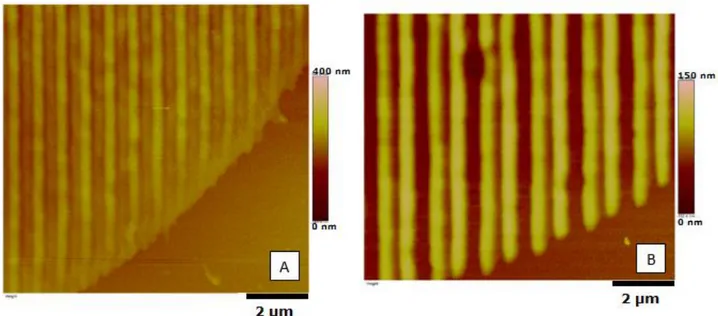
Other than confer chiral properties to a 3D structure, I investigated the possibility to include metallic parts in polymeric structures or to create three-dimensional objects made only by metal nanoparticles. Therefore, I carried out a study on the characteristics of the voxel of a gold-doped PVA resist. My samples are made by sets of single segments, each one obtained with a single laser sweep, on a glass substrate. Upon the exposure, GNPs are created inside the swept segment. I find that the width of each segment depends on the delivered energy dose, as expected. Samples were developed in distilled water in order to
13
remove all the PVA from the substrate and obtained stripes of free GNPs on the glass substrate, on which I performed a basic statistical analysis based on scanning electron microscopy (SEM) images, showing the possibility to control the size and the density of the created GNPs.
These results demonstrate that beyond the bare photochemistry, other effects, which occur during the 2P-DLW process, have to be taken in account to actually describe the GNPS creation. I performed a series of experiments aimed to elucidate the involved physical phenomena, beyond the optical absorption. In particular, I pointed out the key-role of thermal and diffusive processes. TPA leads to the two-photon photo-reductions of ions of AuCl4--, to create GNPs, as well as, to a local heating of the sample that can trigger a thermal
shock-wave, responsible of the local dehydration in the spot area.
Due the concentration gradients of the ions of gold precursor and of water, various diffusive processes taking place at different scale time are observed as well: respectively of 0.1 s for the ion diffusion and of 10 s for the water diffusion, in the hydro-polymer. Therefore, I created GNPs by dosing the energy in multiple shots, considering different time intervals between consecutive laser shots.
My experiments demonstrated that by waiting less than 0.1 s between consecutive shots, no relevant changes are observed. However, waiting a time between 0.1 s and 1 s, the diameter of the spot size changes considerably, as well as density of GNPs. A waiting time of 10 s or more allows the complete rehydration of the area of interest, therefore shooting again in the same spot causes repeatedly the local evaporation of water. This results in a series of thermal shock-waves whose effect cumulates and eject radially the gold nanoparticles form the spot to the near area. In this way, around the spot is formed a ring of GNPs and tetra-chloroauric acid crystals, due to precipitation of the acid in correspondence of the evaporated area. Therefore, I also made an attempt to evaluate the temperature distribution in the area of interest, as a function of the energy delivered. According to my best knowledge, it is the very first experiment that allowed for a temperature mapping at the nanoscale, and whose results are consistent with theoretical predictions present in the literature [200].
14
From my results, it turns out that to obtain the best resolution in the creation of 2D structures made of gold nanoparticles, thermal effects have to be minimized to avoid consistent alterations of the system, and a fine control on the ionic diffusion is required.
To this purpose, I prepared electrolytic cells made of ITO electrodes, in which I infiltrated a solution of water and HAuCl4 and direct laser wrote few 1D segments of 150 μm at an energy dose that was sufficient to activate the seeding process of TP-photo-reduced gold ions, but not the growing process of GNPs. [129]
Growing of gold nanoparticles was performed by applying an electric potential difference between the two electrodes, well below the electro-chemical reduction threshold. The resulting electric field allows controlling the surface density of the ionic species of interest, both for the seeding and the growth phases. Regarding the last, I consider that in proximity of a gold seed a tip effect is obtained, “driving” the gold ions toward the seed, where they are reduced through autocatalytic processes. Analyses on the stripes confirmed a voxel size comparable to the laser beam waist, and that the gold nanoparticles TP-photo-reduced are mono-dispersed, demonstrating that and a control on the GNPs density ad size is obtainable.
Chapter 4
Bi-dimensional structures rich in gold nanoparticles may be used in a wide range of applications, e.g. the laser-nanostructure interaction has become of great interest, in recent years, due to the application of NPs in different fields and their optical properties.
I focused my interest on photo-thermal effect in plasmonic nanoparticles: optical excitation and non-radiative relaxation of the LSPR create a photo-thermal effect due to the conversion of light energy into heat. Within this LSPR-mediated heating process, the light absorbed by the nanoparticle generates a non-equilibrium electron distribution that decays via electron-electron scattering. The hot electron gas equilibrates with lattice phonons, which transfer this energy into the surrounding medium, resulting in a local temperature increase.
15
In a first step, I analysed the heating effects obtained on a huge number of randomly distributed GNPs fixed on a glass substrate, after deep immersion in a gold colloidal solution.
Further thermo-plasmonic experiments were carried on two-photon direct laser written pattern of gold nanoparticles. The possibility to fix gold nanoparticles on a flat substrate, in appropriate design, with a resolution down to a few hundreds of nanometers, pave the way to the fabrication of thermo-smart platforms, able to generate a desired value of temperature by controlling the number of GNPs photo-excited at the same time. Therefore, I carried out careful analysis of the macroscopic photo-induced heat generation of four different 1D gratings of GNPs, created each of them in an area of 1 mm2 and spaced
by 0.5 – 2 – 10 and 100 µm. In particular, it was observed the possibility to tune finely the temperature variation, from 6 °C to 55 °C according to the model used and the intensity of the impinging laser.
Finally, I present preliminary results on the capability of 1D gratings, made by stripes of GNPs to work as surface-enhanced Raman spectroscopy (SERS) substrates. Multiple gratings were created by using different values of laser power and scan speed, and the SERS properties of each structure have been tested against rhodamine-6G and xylene. Enhancement factors (EF) superior to 104 have been quantified.
16
1
Micro- and Nano-fabrication through single and multiple
photons absorption
1.1 Single-photon photo-lithography
Optical lithography is one of the most used and developed micro-fabrication technique [164-166]. The technique is based on the use of a photo-resist: a mixture of a reactive monomer, a solvent and a photo-initiator, spread in liquid phase onto a solid substrate. By tuning the resist viscosity when a spin-coating process is used, a thin film, of thickness finely controlled, typically in the range 0.5 - 100 m, is deposed on a substrate. On such film, features are impressed with ultraviolet (UV) light exposure through a mask. Resists are available in positive and negative tone. A hole in the mask will create a hole in a positive tone photoresists, whereas it will create a pit in a negative tone photoresist. [166]
Let us focus on this last family (the other behaves in the symmetrical way): when a negative tone photo-resist is irradiated with ultraviolet light, the photo-initiator creates free radicals, whose interaction with the nearby monomers generates a crosslinking chain reaction. Polymerization keeps on propagating until either two different interacting radicals form a stable species, or the radicals are quenched due to interaction with non-inert gas present on the environment. To obtain high-quality results, polymerization has to occur completely during the UV light exposure. Therefore, it is mandatory to perform the process under an inert gas atmosphere and to exactly tune it according to the characteristic of the selected photo-resist.
It has to be considered that photo-lithography works efficiently if applied on thin film. Light goes through the holes inside of the mask, but diverts inside the bulk of the photoresist film, according to its thickness.
The mask screens the areas of the film that aren't to be exposed and structures 1D or 2D can be created in the photo-sensitive resin, with a resolution down to few micrometers, diffraction limited. The exposed resin polymerizes and the remaining non-exposed material
17
is removed bathing the sample in a solvent. As a result, it is obtained a strongly adhering layer of controlled thickness, structured in islands reproducing the shape of the uncovered areas in the mask.
This pattern can be hence used as a protective layer in a subsequent wet hatching process, as in the case of the silicon chips in the microelectronic domain, or as a mold in order to imprint the features in another material (soft lithography) [166]. The last is the standard technique used for fabricating microfluidic devices, where the microfluidic network is impressed in a polydimethylsiloxane (PDMS) block. PDMS is the most widely used silicon-based organic polymer, and is particularly known for its unusual rheological properties, allowing to fill and reproduce even the finest details, down to few nanometers. Because of his chemical-physical properties, PDMS is widely used in microfluidics [156-159], opto-fluidics [160-161] and bio-technologies [162], as it is optically clear and biocompatible.
In order to test and to assess the technique, I've prepared three different PDMS molds made as: a network of circular holes with diameter and depth of 30 µm, a network of rectangular holes (30 x 60 x 30 µm3) and a 1D grating made by stripes oh thickness and
height 30 µm.
The resist used to prepare the negative mold of the desired designs was SU-8 2050 (from MicroChem). SU-8 is a family of commercial negative photo-resist, available in different viscosities, according to the dilution of the monomer. The one used is specially tailored for creating films with thickness in the range of 40-170 µm, as a function of the spinning speed.
As substrates, I used standard 76.2 x 25.4 x 1.1 mm3 microscope glass slides,
hydroxylated through a bath in a fresh piranha solution prepared by mixing three parts of sulphuric acid (H2SO4) with one part of hydrogen peroxide (H2O2). The substrates were then
rinsed with deionized water and left to dry. Before deposing 3 mL of photo-resist on each of them, the surfaces were activated through a plasma cleaning process of 5.5 W @ 8 minutes. A two step spin-coating cycle at 500 rpm for 10 s, and then at 4000 rpm for 30 s allowed to
18
obtain a plain film of 40 μm thickness. According to the SU-8 protocol, the film was pre-baked on a hot plate at 95 °C for 5 minutes, to let all the remaining solvent to evaporate.
A chrome on glass mask, with the desired patterns, was put upon the cooled photo-sensitive films (Figure 1.1 A), taking care to face the chrome side to the resist film. Polymerization was performed by using a led UV source (λ = 365 nm), with output intensity of 1.18 mW/cm2 and exposure time of 10 min. A post-exposure baking at 95 °C for 5 minutes
was performed in order to complete the polymerization of the exposed areas.
The film was left to cool for 10 minutes, and developed in a bath of 1-Methoxy-2-propyl acetate for 5 minutes, then the solvent was washed out with a bath in iso1-Methoxy-2-propyl alcohol (IPA) for 10 seconds (Figure 1.1 B). An hard-backing step at 145 °C for 30 minutes was carried out to better fix the structures on the substrates and to ensure that their mechanical properties don’t change during thermal treatments.
Figure 1.1 Scheme on how to prepare a PDMS mold. A) A mask made in chrome (indicated
in brown) has to be put upon a SU-8 film (light blue in the scheme), in order to protect all the areas that have not to polymerize, during the UV exposure. B) The development process chemically removes all the non-exposed material, therefore a negative stamp of the mold in SU-8 is obtained.
A B
19
C) PDMS (indicated in yellow) is poured on the mold to create a layer 5 mm thick and thermally
cured. D) When hardened, the PDMS layer is peeled off from the SU-8 template.
A sufficient quantity of PDMS was prepared by mixing twelve parts in weight of base with one part of curing agent. The mix was put under low vacuum for degassing (0.37 mbar), in order to prevent the appearing of air bubbles in the bulk. Hence a PDMS layer about 5 mm thick was poured onto the SU-8 template (Figure 1.1 C) and left to cure @45 °C overnight. PDMS blocks were finally peeled off from the molds (Figure 1.1 D).
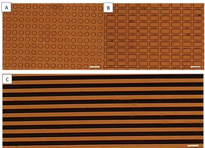
Figure 1.2: PDSM molds, made by A) cylindrical and B) rectangular holes, and C) stripes.
The white line bar in the images is of 100 μm.
Optical images of the three PDMS imprinted structures, are shown in Figure 1.2. I was able to obtain the desired patterns.
A B
20
1.2 Two-Photon Absorption
Direct laser writing (DLW) is a laser scanning fabrication technique allowing to maskless print structures into a photoresist, with a resolution depending solely on the output power and beam waist of the used laser beam [1-3]. When the optical absorption is governed by single photons processes, this technique allows for 3D patterning with resolutions down to typically few microns, in the same order of that given by the mask lithography. A huge improvement is achieved combining DLW with the two-photons absorption (TPA). In fact, exploiting the dependence of the TPA on the squared intensity and the presence of a threshold, features of hundreds nanometers, thus well below the diffraction limits can be created.
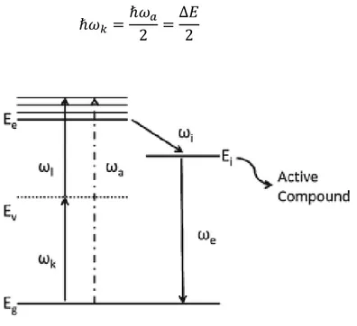
TPA is an optical process, theoretically predicted in 1930 by Maria Goeppert-Mayer [167], and then experimentally observed in 1961 by Kaiser and Garret [168]. As shown in Figure 1.3, a photon absorption excites a molecule from the ground energy level to a singlet excited energy level 𝐸𝑒, according to the process:
Δ𝐸 = 𝐸𝑒− 𝐸𝑔 = ℏ𝜔𝑎
Where ℏ is the reduced Planck constant, 𝜔𝑎 is the angular velocity of the absorbed photon.
The excited singlet level is typically unstable, therefore the system may lose energy and decay to a more stable intermediate energy level 𝐸𝑖, from which it may create a chemical bonding with other activated molecules, or it may release energy in a radiative (through an emitted photon which will have 𝜔𝑒 < 𝜔𝑎), or non-radiative (local heating) way.
According to the Goeppert-Mayer’s theory, the molecule may also be excited by the simultaneously absorption of two photons ℏ𝜔𝑘 and ℏ𝜔𝑙. This is a optical non-linear process involving the third order susceptibility, much smaller the main term responsible of the ordinary optics. Therefore, in order to observe TPA, a huge photon density is required [1-3], as in the case of a tightly focused laser beam. In general, TPA has to fulfil the condition:
21
Δ𝐸 = ℏ𝜔𝑎 = ℏ𝜔𝑘+ ℏ𝜔𝑙
In this case, the system is firstly excited to a virtual level 𝐸𝑣, whose lifetime Δ𝑡~ℏ/Δ𝐸𝑘 is typically in the order of 10-15 s, and then to the excited level 𝐸
𝑒. If a single laser source is used, each photons has energy:
ℏ𝜔𝑘 = ℏ𝜔𝑎
2 =
Δ𝐸 2
Figure 1.3 Energy level diagram for a molecule excited by a single photon (dotted line) or by
two photons (straight line), from the ground level to an excited level. In both case, the compound may be activated or may release energy through radiative or non-radiative processes. [1]
The activation rate through TPA is strongly different in respect to the single photon absorption (SPA). For organic photo-resist, typical values of the SPA cross-section 𝜎 are in the order of 10-16 cm2, while the TPA cross-section 𝜎
2 is in the order of 10-50 cm4s [1]. The SPA cross-section 𝜎 can be calculated according to Beer’s law:
𝐼(𝑥) = 𝐼0𝑒−𝛼𝑐𝑥
(1.2)
(1.3)
22
Where: 𝐼 is the laser intensity, 𝛼 = 𝜎𝑁 is the SPA absorption coefficient, N is the molecular number density, c is the molecular concentrations and x the path length. In the TPA case the eq. (1.4), becomes:
𝐼(𝑥) = 𝐼0 1 + 𝛽𝑐𝑥𝐼0
In which 𝛽 = 10−3 (𝜎2 𝑁𝐴 𝑐)/ℏ𝜔 is the TPA absorption coefficient, 𝑁𝐴 is the Avogadro number, and 𝜎2 the TPA cross-section. If follows that 𝜎2 is a function of the square of the laser intensity [2].
1.2 Two-photon Polymerization
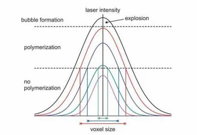
Through the TPA process, when an ultrafast near infrared (NIR) laser is focused on a UV-sensitive resin, polymerization is activated only in a very small volume inside the focus. This is the smallest polymerizable volume, usually called volume pixel (voxel) and defines the resolution of the photo-polymerization process [1-3].
Two-photon polymerization (TPP) presents two energy thresholds, as shown in Figure 1.4. The first one is the polymerization threshold, which depends on the laser intensity and the material cross-section 𝜎2. Only the portion of the Gaussian profile of the laser intensity that exceeds the threshold leads to local polymerization. Thus, the voxel dimensions strongly depend on the incident laser beam intensity. The second threshold is defined by the onset of the optical breakdown of the polymer: when the laser intensity is higher than this threshold, explosions can even occur and the resin is permanently damaged.
23
Figure 1.4: Laser intensity dependency of the voxel size. If the laser intensity is below the
polymerization threshold no polymerization happens, else only the portion of the Gaussian beam higher than the threshold will lead to the voxel polymerization. Over the second threshold, the resist explodes and is permanently damaged [1].
Sweeping the laser beam into the photo-resist, is thus possible to create bi- and three-dimensional polymeric structures, whose resolution is given by the size of the voxel. A prediction of the diameter and length of a voxel is thus necessary to create refined 3D objects. The diameter 𝑑 and the length 𝑙 of the voxel are:
𝑑(𝑃, 𝑡) = 𝑟𝜔0√ln (4 𝑃 2𝑡 𝜈𝑡𝐿(𝑟𝜔02𝜋 ∙ ℏ𝜔)2 𝜎2 ln (𝜌 𝜌0 0− 𝜌𝑡ℎ) ) 𝑙(𝑃, 𝑡) = 2𝑧𝑅√√(4 𝑃 2𝑡 𝜈𝑡𝐿(𝑟𝜔02𝜋 ∙ ℏ𝜔) 2 𝜎2 ln (𝜌 𝜌0 0− 𝜌𝑡ℎ) ) −1
The voxel length and diameter depend then on the laser power 𝑃, the exposure time 𝑡 and the TPA cross-section 𝜎2. The other terms are related to the materials and optical system used. 𝑟𝜔0= 0.61 𝜆/𝑁. 𝐴. is the beam waist, 𝑧𝑅 = 𝜋𝑟𝜔02/𝜆 is the Rayleigh length, 𝜈 the pulsed laser repetition rate, 𝑡𝐿 the single pulse width, ℏ𝜔 the energy of the incident
(1.5)
24
photon, 𝜎2∗ = 𝜎2/𝑙𝑛[𝜌0/(𝜌0− 𝜌𝑡ℎ)] is the effective cross section for the TPA, 𝜌0 and 𝜌𝑡ℎ are the initial density and the threshold density of radicals respectively.
1.4 TP-DLW
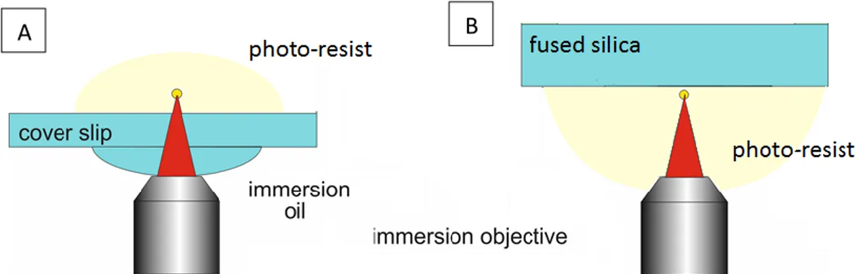
The TP-DLW system used presents a femtosecond Ti:Sapphire (λ = 780 nm) laser connected to an inverted microscope. The laser beam is focused on the sample through a 63x or 25x objective, with N.A. respectively of 1.4 and 1.1. 3D structures can be fabricated both through the glass, and by the diving the objective in the resist (Figure 1.5).
Figure 1.5 Scheme of the writing process A) through the glass, B) by immerging the objective
inside the photo-resist.
During the printing process, the working distance of the objective (typically 350-400 μm) has to be taken in consideration when the TP-DLW is performed through the glass. Moreover, since the writing process occurs plane by plane, to create the highest parts of a structures, the laser beam has to go through the objects already created and is attenuated, generating smaller effective voxels.
By working with the objective immersed in the resin, it is possible to create 3D object with theoretically no vertical limits. However, fluid-dynamic effects may occur while moving the lens and affect the final result.
25
1.4.1 Modelling
To print a three-dimensional object, a 3D computer-aided design (CAD) software is preferable. In Figure 1.6 A is shown the example of the 3D model of the logo CNR Beyond-Nano Cosenza. In order to perform the printing, the model is sliced in layers (Figure 1.6 B), whose thickness has to be set accordingly to the voxel z-length, or they won’t adhere each other.
Each plane is hatched in single segments (Figure 1.6 C), whose width has to be set accordingly to the voxel diameter.
It is than evident that a thorough study on the voxel dimensions in function of the laser intensity and exposure time has to be carried out for each used photo-resist.
A
26
Figure 1.6 A) CAD model of the CNR Beyond Nano Cosenza logo, B) sliced in planes and then C) hatched in crossed lines.
1.4.2 Analyses.
Here is discussed the characterization of the voxel generated by diving the lens into the commercial photo-resist IP-Dip, whose refractive index is 1.52, matching that of the frontal lens. On the contrary, a refractive index mismatch between the photo-resist and the substrate is required to locate the interface, i.e. the z = 0 position. Therefore, a substrate of fused silica (refractive index: 1.46) was used.
In Figure 1.7 is shown the matrix of 1D gratings printed with the 63x, N.A. 1.4 objective, in order to characterize the voxel size.
27
Figure 1.7 Scheme of the matrix of 50x50 μm2 1D gratings printed. Each grating has period
of 0.5 and μm was printed, using different values of laser power (20 - 40 mW, step 5 mW) and scan speed (2.5 x 10⁴ - 1.5 x 105 μm/s, step 2.5 x 104 μm/s).
To remove all the non-exposed resist, after the printing process, the sample was developed through a bath in propylene glycol monomethyl ether acetate (PGMEA) for 25 minutes, and then in IPA for 5 minutes. When the sample dried, the gratings were analysed by means of scanning electron microscope (SEM) and atomic force microscope (AFM).
SEM is a well-known probing technique, which allows analysing objects, whose size is below the diffraction limits [169]. Briefly, the sample is probed with an electron beam. The electrons interact with the sample elastically (back-scattered electrons, BSEs) or lose their energy through multiple random scatterings, inside the interaction volume, which leads to the emission of secondary electrons (SEs) and X-ray radiation [169]. Different detectors may be used to collect the various signals, the BSEs provide information on the atomic number of the sample, the SEs on the topology, and the X-ray radiation on the atomic composition allowing the possibility to perform energy dispersive X-ray (EDX) analysis on the surface.
28
AFM allows to measure the three-dimensional profile of sub-micron objects. A tip, typically tall 5 μm and with a ending radius of 5 nm scan the object, reproducing its profile. The Wan der Vaals forces rule the interaction between the tip and the sample, thus the morphological analysis of any kind of solid surface is permitted [170].
An example of SEM and AFM imaging on a grating printed with laser power 20 mW and scan speed 7.5 x 104 μm is shown in Figure 1.8.
Figure 1.8: A) SEM image of a 1D grating created with laser power 20 mW and scan speed
75 x 104 μm/s. SEM allows to get best information on the spatial resolution, while AFM on the
three-dimensional profile.
Combining the data obtained by SEM and AFM imaging, it is possible to characterize the voxel size of the photo-resist in function of the printing parameters.
29
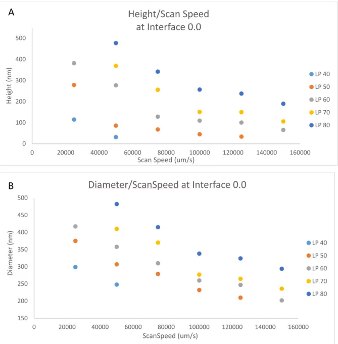
Figure 1.9 A) Length and B) Diameter of a voxel dependence on the scan speed of the laser
beam during the writing process, measured for different laser power values.
In particular, according to Eq. (1.5) and Eq. (1.6), the effective cross-section of the photo-resist IP-Dip is 𝜎2∗ = (3,0 ± 0,8)10−52𝑐𝑚4𝑠. Moreover, I was able to define the polymerization and explosion thresholds, obtaining d = 200 nm and l = 80 nm as dimensions of the smallest polymerizable voxel and d = 480 nm and l = 960 nm for the largest one (Figure 1.9).
However, the AFM profile of the largest voxels does not reveals a Gaussian shape, in contrary to smaller ones. In Figure 1.10 A and B, the example of the voxels obtained by
0 100 200 300 400 500 0 20000 40000 60000 80000 100000 120000 140000 160000 He ig h t (nm )
Scan Speed (um/s)
Height/Scan Speed
at Interface 0.0
LP 40 LP 50 LP 60 LP 70 LP 80A
150 200 250 300 350 400 450 500 0 20000 40000 60000 80000 100000 120000 140000 160000 Diame ter (n m ) ScanSpeed (um/s)Diameter/ScanSpeed at Interface 0.0
LP 40 LP 50 LP 60 LP 70 LP 80B
30
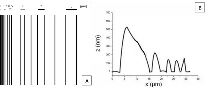
printing two stripes at scan speed 7.5 x 104 μm/s and laser power respectively 20 mW and
40 mW are compared. Writing patterns with dense hatching, low velocities and high laser power values, leads to an enhancement of the local temperature, which can trigger the cross-linking of the monomers in the surrounding volume. As a consequence, adjacent segments appear as a bigger single stripe or a connected by a polymeric filamentation (Figure 1.10 C-D).
Figure 1.10 AFM profile of a single line of a 1D grating printed in IP-Dip @ 7.5x 104 μm/s and
laser power A) 20 mW and B) 40 mW. C) SEM image of the latter gratings, with D) a bottom edge detail. Adjacent stripes written at high energy can be connected by a thin polymeric filamentation or two lines can generate a bigger one.
When one wants to print 3D microstructures has to take this effect in consideration: due to the linking between two different stripes, the final structure results more solid, but
A B
31
the resolution worsens. Moreover, the temperature increases layer by layer and explosion may occur.
From this analysis, to write 3D solid object with high resolution in IP-Dip, I selected as best condition laser power 25 mW, scan speed 1.25 x105 μm/s, hatching 0.2 and slicing,
0.1.
Figure 1.11 AFM imaging of the CNR Beyond-Nano Cosenza logo printed in IP-Dip, by
selecting laser power 25 mW, scan speed 125000 μm/s, hatching 0.2 and slicing, 0.1. The logo is 50.0 μm x 21.0 μm x 0.5 μm, with features well below the diffraction limit.
E.g. I used these parameters to print the model in Figure 1.7. The AFM profile shows that the structure is (50.0 x 21.0 x 0.5) μm3, with features inside the word ‘Cosenza’ in the
order of 600 nm, and the thickness of each letter is 800 nm (Figure 1.11). The resolution of the logo is ~200 nm, well below the one obtainable through photolithography.