CHAPTER 1
Silicon bulk-microstructuring technology for high complex microsystem and microstructure fabrication: a review
Abstract
In this chapter silicon (Si) bulk-microstructuring technologies for fabrication of high complex microsystems (Si-HCMs) are reviewed, including advantages, and limits, basic physical properties, geometrical features of feasible microstructures, applications and required equipment/setup. Firstly, technologies for Si-HCMs are analyzed starting form well established technologies, such as wet anisotropic etching in alkaline-based solution and dry etching process. Secondly, a novel emerging silicon microstructuring technologies, such as electrochemical micromachining (ECM) in hydrofluoric acid electrolyte and laser etching are discussed.
Key specifications are high aspect-ratio (HAR) microstructures, good trench sidewall profile with smooth surface, and possibility of producing three dimensional (3D), as well as free-standing (FS) microstructures.
1. Introduction
The fabrication of high complex microsystems integrating three-dimensional (3D), free-standing (FS), and high aspect-ratio (HAR) silicon microstructures with arbitrary shape at low cost is of relevance for a multitude of research topics and commercial applications, such as energy harvesting, [1] lab-on-a-chip fabrication [2], and 3D microchip stacking [3].
Micromachining tools have been developed for half a century with the aim of structuring silicon at microscale level, always breaking new research/market grounds. Since the early 1960s, wet etching technology, both isotropic and anisotropic, has driven micromachining research/industry (e.g., inkjet cartridges, chromatographic columns, microtip arrays, etc.), thanks to its straightforward and low-cost approach, though it is characterized by a limited flexibility in fabrication and low integration density [1].
In the 1980s, the demand for increased flexibility in fabrication and higher integration density, driven by novel challenging applications (e.g., MEMS, lab- on-a-chip, “through-silicon-via” (TSV), etc.), pushed micromachining research/industry towards the development of dry etching technology with higher performance, although higher cost too [15]. Both wet and dry technologies are still under development, with wet technology being mainly used for the fabrication of
undemanding microstructures with a low density at lower cost, and dry technology exploited for the fabrication of complex microsystems with increased density at higher cost.
Other potential technologies for Si-HCMs fabrication include hybrid technologies that are obtained by combining wet and dry etching, laser etching and a novel emerging wet technology namely electrochemical micromachining (ECM).
2. Wet anisotropic etching
Since the early 1960s, when silicon etch was found to be both crystal orientation and concentration-dependent in some chemical solutions, wet anisotropic etching of silicon in alkaline-based solutions such as, potassium hydroxide (KOH), tetramethyl ammonium hydroxide (TMAH), ethylene diamine pyrocatechol (EDP) and others, has become a highly developed and well established technology for fabrication and prototyping of silicon microstructures and microsystems [7,8]. 2.1 Origin of silicon etching anisotropy in alkaline solutions
Anisotropy of silicon etching in alkaline-based solutions is manly due to the crystalline structure of silicon material (crystalline silicon – c-Si), which determines difference in chemical, and physical properties (i.e. surface density of silicon bonds, bonding energy of silicon atoms etc.) of different crystal planes thus yielding different oxidation rates. When silicon is rinsed in alkaline-based solution containing an oxidizing agent, silicon oxidation and etching occur simultaneously; as a result, different crystallographic planes (e.g., (110), (100), and (111)) were etched at different rates. As an example, KOH displays an etch rate up to 400 times higher for (100) crystal directions than (111) directions [9,10]. EDP (an aqueous solution of ethylenediamine and pyrocathecol), displays a (100)/(111) selectivity value of about 20, does not etch silicon dioxide as occur for KOH etching, and also displays high selectivity between lightly doped and heavily boron-doped (p-type) silicon [9,10]. However, KOH may introduce mobile potassium ions into silicon dioxide so that KOH etching results incompatible with CMOS process. On the other hand EDP is highly corrosive and carcinogenic, so care is required when dealing with such etchant. TMAH represents a safer and CMOS compatible alternative than EDP and KOH based etching technology, with a selectivity of about 30 between (100) and (111) planes in silicon [9,10].
From here-to-after, we refer for simplicity to KOH etching process and the specific nature of alkaline etchant will be not further discussed in this chapter, which is focused on reviewing state-of-the-art of silicon microstructuring with specific attention to technology able to produce high complex silicon microsystems/microstructures.
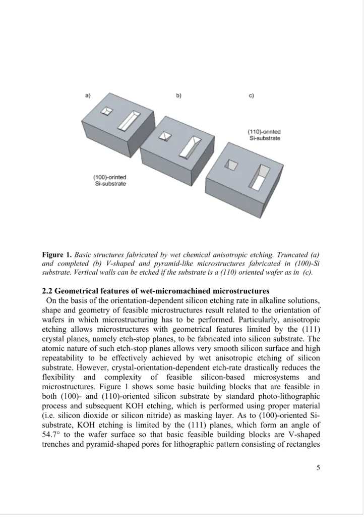
Figure 1. Basic structures fabricated by wet chemical anisotropic etching. Truncated (a) and completed (b) V-shaped and pyramid-like microstructures fabricated in (100)-Si substrate. Vertical walls can be etched if the substrate is a (110) oriented wafer as in (c). 2.2 Geometrical features of wet-micromachined microstructures
On the basis of the orientation-dependent silicon etching rate in alkaline solutions, shape and geometry of feasible microstructures result related to the orientation of wafers in which microstructuring has to be performed. Particularly, anisotropic etching allows microstructures with geometrical features limited by the (111) crystal planes, namely etch-stop planes, to be fabricated into silicon substrate. The atomic nature of such etch-stop planes allows very smooth silicon surface and high repeatability to be effectively achieved by wet anisotropic etching of silicon substrate. However, crystal-orientation-dependent etch-rate drastically reduces the flexibility and complexity of feasible silicon-based microsystems and microstructures. Figure 1 shows some basic building blocks that are feasible in both (100)- and (110)-oriented silicon substrate by standard photo-lithographic process and subsequent KOH etching, which is performed using proper material (i.e. silicon dioxide or silicon nitride) as masking layer. As to (100)-oriented Si-substrate, KOH etching is limited by the (111) planes, which form an angle of 54.7° to the wafer surface so that basic feasible building blocks are V-shaped trenches and pyramid-shaped pores for lithographic pattern consisting of rectangles
and squares respectively (Figure1(a)). As to (110)-oriented silicon substrate, (111) crystal planes are orthogonal to the wafer surface, so that structures with very vertical sidewall can be effectively fabricated thanks to high selectivity (up to 400) between etch-rate of (100) and (111) crystal planes (Figure 1(b)).
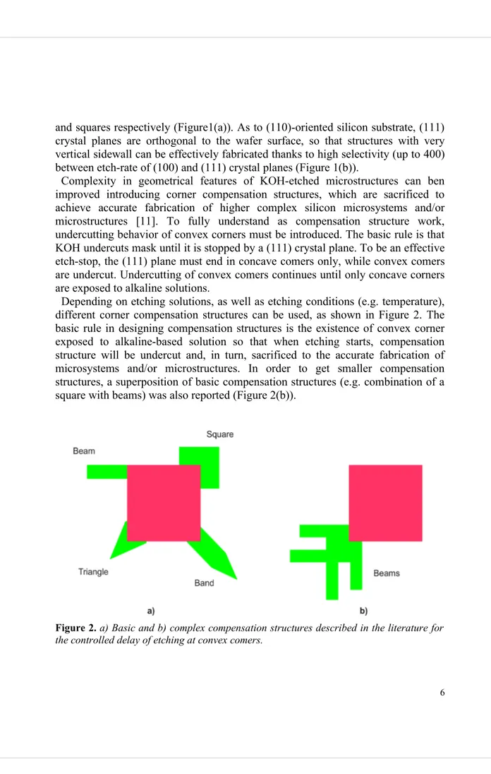
Complexity in geometrical features of KOH-etched microstructures can ben improved introducing corner compensation structures, which are sacrificed to achieve accurate fabrication of higher complex silicon microsystems and/or microstructures [11]. To fully understand as compensation structure work, undercutting behavior of convex corners must be introduced. The basic rule is that KOH undercuts mask until it is stopped by a (111) crystal plane. To be an effective etch-stop, the (111) plane must end in concave comers only, while convex comers are undercut. Undercutting of convex comers continues until only concave corners are exposed to alkaline solutions.
Depending on etching solutions, as well as etching conditions (e.g. temperature), different corner compensation structures can be used, as shown in Figure 2. The basic rule in designing compensation structures is the existence of convex corner exposed to alkaline-based solution so that when etching starts, compensation structure will be undercut and, in turn, sacrificed to the accurate fabrication of microsystems and/or microstructures. In order to get smaller compensation structures, a superposition of basic compensation structures (e.g. combination of a square with beams) was also reported (Figure 2(b)).
Figure 2. a) Basic and b) complex compensation structures described in the literature for the controlled delay of etching at convex comers.
2.3 Wet anisotropic etching of silicon: applications
In this section, examples of microsystem fabricated by exploiting wet anisotropic etching of c-Si substrates are given and detailed, with particular attention to high complex Si-based microsystems. However, the above mentioned crystal-orientation-dependent etch-rate limits flexibility and complexity in microfabrication; thus only few examples regarding this subject are reported in the literature.
Wet anisotropic etching of (100)-silicon substrate was used for the fabrication of V-grooves for alignment of optical fibres in silicon motherboards, as well as for fiber coupling in integrated optics [13]. Moreover, in [15,20] wet anisotropic etching of silicon substrates was successfully used for fabrication of microfuidic Si-based networks/devices for Lab-on-Chip and (Bio)chemical/biological applications.
Fabrication of deep vertical trenches by wet anisotropic etching of (100)-oriented Si substrate was also reported [14-15,20]. Particularly, in [14] KOH etching was used for the integration of one dimensional (1D) photonic crystal (PhC) as well as 1D-PhC-based Fabry-Perot microcavity with highly smooth silicon sidewalls, together with grooves for optical fiber positioning/alignment in front of 1D-PhC structures ( Please see Figure 3).
Figure 3. (a) SEM image of the photonic crystal with in-plane fiber grooves fabricated by wet anisotropic etching of (110)-silicon substrates [14].
Figure 4. SEM micrograph of free-standing crystalline silicon cantilever structure with integrated V-groove [35].
Finally as an example of complexity in wet-anisotropic microfabrication we report an optical moving-fibre switch with bistable operation [36]. The authors demonstrated fabrication of very precise alignment structures which are necessary for single-mode fibre devices and large displacement actuators in a single wet etching step (Fig. 4).
2.3.1 Silicon-on-Insulator: the way to increase complexity in Si-microstructuring. Silicon-on-insulator wafers (SOI) are precisely engineered multilayer semiconductor/dielectric structures that could improve complexity and flexibility of both wet and dry etching technologies. Originally discovered in 1966, the SOI wafer is nowadays a widely diffused technology in the field of microelectronics for realization of high-speed, low-power digital and analog/RF CMOS circuits, as well as for some niche applications under extreme high temperature or radiation operating conditions [34].
Recently, SOI wafers have beeen successfully used for fabrication of microsystems suitable for MEMS and MOEMS applications [34-35]. The buried oxide layer of SOI wafer can be successfully used as an etch-stop layer for both wet micromachining technologies, either from back or from front side of the wafer. Moreover, buried-oxide layer of SOI wafers can be easily etched by wet hydrofluoric acid-based (HF) solutions thus releasing top silicon layer in which, micromachined microstructures were fabricated, and, in turn, enabling fabrication of three-dimensional (3D), as well as free-standing (FS) microstructures. The releasing of micromachined microstructures is limited by diffusion of HF under the silicon top-layer of SOI wafers. In order to reduce the releasing time of
microstructures that are integrated on silicon top-layer, an array of holes are commonly introduced in the microsystem layout. By exploiting wet anisotropic etching on (100)-SOI wafer, Graff et al. have demonstrated fabrication of free-standing square-shaped silicon diaphragms [35]. The diaphragms consists of c-Si-based micromirror with an area of 100 μm2, which is suspended by four arms with
dimension of 100 μm x 10 μm.
2.4 Equipments for Wet Microstructuring
Being a wet chemical process, anisotropic etching needs a pretty simple equipment. It basically consists of a glass or teflon vessel in which silicon wafers can be easily placed and immersed in the etchant. Since reaction rate, and, in turn, etching-rate of silicon strongly depends on temperature, the etching solution is commonly placed into a double wall container with thermostated oil between the two walls. The etching temperature is commonly in the range [50-100] °C. In order to avoid etchant evaporation, the vessel is usually closed by a tight cap; the evaporating fluid is caught by a water-cooled reflux condenser. For security reasons, the whole apparatus has to be placed within a chemical fume.
Very often anisotropic etching has to be performed on one side of the silicon wafer while the other side has to be protected. Backside of silicon wafers can be passivated by a full-wafer masking film consisting of materials that are slowly etched in alkaline based solutions (e.g. silicon nitride or silicon dioxide). However, during the etching process, which could take several hours, these films may be etched leading to silicon surface exposed to etchant and, in turn, compromising integrity of silicon wafer. A possible alternative consists in using a holder in which the wafer is packed between two teflon parts. The rear part protects the silicon while the front part is open to etchant. Tightening is usually done with O-rings [21]. In order to avoid diffusion of etchant trough O-ring the space between silicon wafer and glass/teflon chamber can be filled with an inert gas that is maintained in over pressure conditions.
3. Dry Etching
Since the 1980s, impressive progresses have been made in silicon dry etching process, which is nowadays a well established technology successfully employed in several applications, including fabrication of silicon molds, silicon pillars, ridges, optical gratings, Fresnel lenses, actuators, microturbines, microfluidics devices, etc. [23].
A detailed study of state-of-the-art of dry etching technology highlights that there are basically two dry technologies that have emerged over the years as most promising for high complex Si-based microsystems fabrication: cryogenic plasma etching (CPE) and Deep Reactive Ion Etching (DRIE), which is often referred as
Bosch process. In order to fully understand as DRIE and CPE process works a brief consideration about operation principle of dry etching is be introduced.
3.1 Dry: DRIE operation principle
Dry etch process is based on a gas-solid chemical/physical reaction that takes place in presence of an electrically neutral mixture of molecules, atoms, ions, electrons, and photons, which is know as plasma. In particular, plasma is a discharge in which ionization of gases takes place yielding chemically active species, namely oxidizing and/or reducing agents. In presence of high electrical fields, gas molecules ionize producing chemically active species. Different gas mixtures, as well as different mixing ratios give rise to unique etch characteristic and profiles. Details about most commonly diffused etching gases and materials are described in [11]. For dry etching process, two kind of reactions may occur at the wafer/gas interface: chemical etching and physical etching. Chemically active ions can react with silicon (or other materials, such as silicon dioxide etc.) to form a volatile compound that is removed through gas circulating in chamber reactor.
Physically ionized species are accelerated toward the target wafer in which microstructuring has to be performed. Such ions physically bombard silicon substrate, and, in turn, remove atoms from the target. In general, physical etching is more directional and anisotropic than chemical etching, which is usually isotropic and material selective. Compared to other plasma etching processes, RIE process is more physical in nature so that its etch-rate distribution is more anisotropic. However, in order to produce deep and high aspect-ratio features with vertical sidewalls, which are the main task in many practical cases especially for production of high complex silicon-based microsystems, improvements in RIE process are required.
DRIE process is capable to deeply etch silicon by means of repeated cycles consisting of dry etching step followed by a passivation step. In particular, a layer of inhibition materials (i.e. polymeric compounds produced during etching step) is deposited during passivation step on the surface of microstructures grooved into the silicon substrate. During the subsequent etching step, inhibition film is substantially removed at the bottom of microstructures thanks to ion bombardment, while polymer layer on sidewall is only partially removed. Process parameters play an important role in determining morphology and geometrical features of dry-etched silicon surfaces.
3.2 Geometrical features of dry-etched microstructures
Dry etching process is alternative to wet silicon anisotropic etching. Dry etching technology allows high flexibility in designing and microstructuring of Si-based microsystems to be achieved thanks to its substantial independence from crystal orientation of c-Si substrate. In other words, dry etching has potentialities of
producing microstructures with arbitrary shape and high accuracy. Examples of dry-etched silicon microsystems/microstructures such as rounded-shaped microneedles array [18], microfluidic channel/networks [24], valves for autonomous capillary systems [25], etc. have been reported in the literature.
Despite high potentialities of DRIE process for silicon microstructuring, such technology shows some relevant drawbacks that limit its applications especially for fabrication of high complex Si-based microsystems.
The key challenge of DRIE process is the etching of HAR structures with smooth and vertical sidewall profiles with control on secondary effects that affect dry etching process, such as loading effects, aspect-ratio dependent etching (ARDE), micrograss, tilting, and notching. Each one of these aspects is detailed in [23]. However, aspect-ratio-dependent-etching rate (ARDE or Lag-RIE effect) of DRIE and high sidewall surface roughness due to scalloping of alternating etching and passivation steps are the two major problems of dry etching technologies.
3.2.1 Sidewall roughness
DRIE process can be envisioned as a time-multiplexed RIE process, in which an etch step (e.g. SF6 gas) and a passivation step (e.g. C4F8) alternates every few
seconds thus producing sidewall roughness that can be related to the alternating etching and passivation steps.
In order to limit the induced roughness, different sidewall passivation mechanisms were investigated [23]. A feasible way is performing DRIE process with simultaneous and continuous flow of etching and passivation gases thus reducing duration of etching and passivation steps, and, in turn, roughness of sidewall. Even though, reduction of sidewall roughness from a 100-200 nm to 10 nm has been demonstrated, in many practical cases balance of etch and passivation steps, which is critical for achieving a stable anisotropic etching, results compromised thus yielding significant sidewall bowing.
A successful method based on trench sidewall passivation is cryogenic plasma etch (CPE) process proposed in 1988 [23]. Rather than performing alternating etch and passivation steps as in DRIE process, the cryogenic etch process aims to perform these two steps simultaneously using SF6 and O22 gases. Vertical walls with
extremely good quality of the profile are achieved. The passivation mechanism results from the formation of SiOXFY on the sidewalls at low temperatures (lower
than −100 °C) thus preventing roughness during etching. The advantages of this process are low sidewall roughness (a few nanometers), fast etch rate (passivation and etching proceed concurrently), and increased mask selectivity (especially for photoresist and silicon dioxide) due to the low inductively coupled plasma (ICP) bias voltage required [23]. Since roughness is a major limit of DRIE, especially in optical applications, it is expected that CPE could become a major technique of silicon microstructuring within the next few years. Even though cryogenic plasma
etching has special etch properties, such as steady-state process control and low trench sidewall surface roughness, which are essential for some applications, achieving a wafer temperature below −100 °C is expensive and makes etching control more complicated with a respect to DRIE process.
3.2.2 ARDE effect
Aspect-ratio-dependent-etching (ARDE) concerns accuracy in simultaneous fabrication of microsystems integrating microstructures with different aspect-ratio values. ARDE, also referred as to RIE-lag effect, exists in all etch processes but is of particular relevance when fabricating HAR structures. In fact, when etching HAR microstructures with DRIE it is observed that etch rate depends on both time and mask opening. Smaller trenches are etched slower than larger trenches. Indeed, ARDE effect reduces accuracy in fabrication of complex microsystems in which structures with different geometrical features have to be integrated into the same silicon substrate by one-etching step as occurs in several applications of interest (e.g. M(O)EMS applications).
Depletion of fluorine at the bottom of etched microstructures is the root cause for ARDE [23]. The dominant process parameters are thus etchant-gas flow-rate and its dissociation within deep trench. Since ARDE is a result of transport phenomena, it is clearly noticeable that such phenomena increase with the aspect-ratio of structures. This mass transfer rate changes as the etch progresses, thus leading to an etch-rate that decreases with time. A way to overcome ARDE is to change etch parameters as the etch progresses. Gradually, increasing bombarding bias power once the etch depth is deeper than a predetermined value was reported as a successful strategy to reduce ARDE effect [23].
In order to fabricate HAR microstructures, great effort has been put in studying ARDE in a time-multiplexed process (DRIE). By examining ARDE phenomena in three distinct stages of a process cycle (inhibition film deposition, inhibition film etch and silicon etch) it was found that both passivation and etch step are aspect-ratio-dependent [23]. Based on these phenomena, a compensation method between deposition and etch was proposed by adjusting relative times of passivation and etching steps at certain process conditions. Using this approach reduction of ARDE effect, was demonstrated [23]. However, compensation techniques can affect balance between passivation and etching steps thus reducing anisotropy of DRIE process and, in turn the possibility of producing HAR microstructures with vertical sidewall.
3.3 DRIE of silicon: applications
Starting form 1980s, many studies were performed to explore use of dry etching of silicon, with particular attention to MEMS applications [23]. This intensive MEMS development resulted in significant progress in silicon microstructuring.
The great success achieved by dry etching technology is clearly highlighted by the noteworthy theoretical and experimental results reported in the literature on this subject.
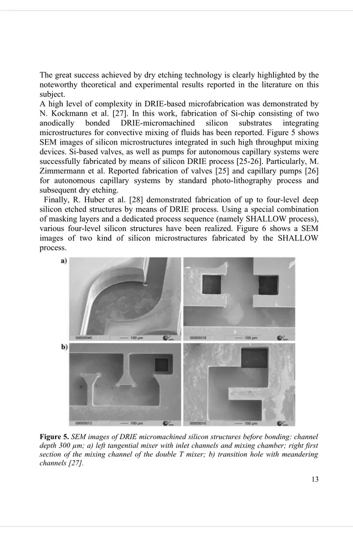
A high level of complexity in DRIE-based microfabrication was demonstrated by N. Kockmann et al. [27]. In this work, fabrication of Si-chip consisting of two anodically bonded DRIE-micromachined silicon substrates integrating microstructures for convective mixing of fluids has been reported. Figure 5 shows SEM images of silicon microstructures integrated in such high throughput mixing devices. Si-based valves, as well as pumps for autonomous capillary systems were successfully fabricated by means of silicon DRIE process [25-26]. Particularly, M. Zimmermann et al. Reported fabrication of valves [25] and capillary pumps [26] for autonomous capillary systems by standard photo-lithography process and subsequent dry etching.
Finally, R. Huber et al. [28] demonstrated fabrication of up to four-level deep silicon etched structures by means of DRIE process. Using a special combination of masking layers and a dedicated process sequence (namely SHALLOW process), various four-level silicon structures have been realized. Figure 6 shows a SEM images of two kind of silicon microstructures fabricated by the SHALLOW process.
Figure 5. SEM images of DRIE micromachined silicon structures before bonding: channel depth 300 µm; a) left tangential mixer with inlet channels and mixing chamber; right first section of the mixing channel of the double T mixer; b) transition hole with meandering channels [27].
Figure 6. Four-level silicon structures fabricated by SHALLOW process, (a) four-level microfluidic devices and 3-D gear wheel (b) [28].
In order to enable high flexibility in microfabrication and high quality vertical surfaces, dry (e.g. DRIE) and wet (e.g. KOH) etchings have been combined for realizing Si-based HC microsystems, in which DRIE-etched microsystems with high aspect-ratio are post-processed by KOH etching to improve surface quality of optical structures [29-31]. Though significant improvements of the quality of DRIE-etched surfaces have been demonstrated by KOH post-processing (surface roughness reduced up to one order of magnitude), others drawbacks of dry etching technologies in the out-of-plane direction (e.g. deviation from verticality, ARDE problems, etc.) are not easily addressable with this approach.
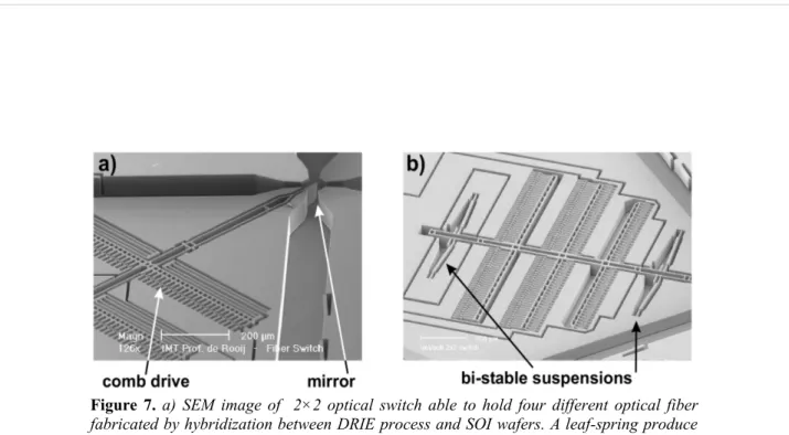
Particularly interesting is the combination of DRIE process with the use of SOI wafer. In this case buried silicon oxide layer of SOI wafers can be removed yielding free-standing structures with deep vertical walls. Such approach has been successfully employed in fabrication of high complex Si-based microsystems such as both capacitive and optical accelerometers [37], gyroscopes [38], electrostatic actuated microgripper [39], electrostatic tunable optical switch and mirror for optical communications applications [37, 40], array of microcantilever array for data- storage or biosensing applications [41,42], etc. N.Wilfried et al. [37] demonstrated fabrication of an optical switch for telecomunication applications. Figure 7 shows a SEM image of both mono-stable and bi-stable configuration 2 × 2 optical switch able to hold four different optical fiber. The images clearly highlights that fry etching into SOI wafers allows high complexity in microfabrication to be effectively achieved.
Figure 7. a) SEM image of 2×2 optical switch able to hold four different optical fiber fabricated by hybridization between DRIE process and SOI wafers. A leaf-spring produce suspension of beam that holds a silicon mirror. b) SEM image of a 2x2 optical switch in a bi-stable configuration. In both devices optical fibers are held by small leaf-springs that are integrated sidewall of U-grooves [37].
Summarizing, combination between wet/dry anisotropic etching technology and SOI wafers allows both high flexibility in designing and high complexity in fabrication of silicon microsystems to be effectively achieved. However, such approach does not overcome the major drawbacks of both wet and dry technology, which are mainly low flexibility and complexity in microfabrication and both ARDE effect and high roughness of sidewall surface respectively.
3.4 Equipments for dry (DRIE) microstructuring
Several standard systems are available for performing plasma-based etching proces. Despite DRIE process belongs to the family of induced coupled plasma (ICP) etching techniques, there are a number of significant features of equipment used for DRIE process which differ from normal ICP systems.
First of all, fast pumping mechanism are required to achieve high flows of process gases and, in turn, high etch-rates. This implies the use of a large capacity turbo-molecular pump that is connected to an appropriate high capacity rotary pump. Moreover, fast response of mass flow controllers is required to perform time-multiplexed etching process with very short times step.
Times step can be furthermore pushed reducing delay time between mass flow controllers opening and gas reaching. To achieve such goal, DRIE equipments exploit short mixed gas line between mass flow controllers and process chamber. Operation principle of DRIE process suggests as uniformity of plasma within ICP region is crucial to produce uniform etching profile. A strategy to give better uniformity of plasma within ICP region consists in implementing a pure inductive
coupling of power in the ICP region, instead of total capacitive or partially capacitive coupling, which causes differences in ion density that affects profile uniformity.
Finally, walls, lid, and pump lines of DRIE equipments should be heated thus reducing deposition of volatile compounds (e.g. fluorocarbon polymer) that could flake and fall as particles on the wafer. It also minimizes the deposition of volatile compounds in pumping lines, as well as, on turbo-pump.
4. ECM
Originally discovered by V. Lhemann and Föll, electrochemical micromachining (ECM) technology, commonly used for regular macropore formation [44,45], only recently has been assessed as a powerful method for fabricating a multitude of silicon microstructures, with applications to microelectronics [46], space [47], optics [48-51], and microfluidics [52]. ECM fabrication of MEMS structures consisting of free-standing inertial masses anchored by springs to the silicon substrate, as well as mechanical microgrippers has been recently demonstrated [53]. ECM technology combines advantages of both dry (high-flexibility) and wet (low-cost) standard silicon etchings. It represents today a unique case of straightforward, low-cost, wet-etching technology with microfabrication flexibility typical of complex, high-expensive, dry-etching processes. Among the main features of ECM there are: i) high aspect-ratio of feasible structures, up to 500, and in turn high integration density; ii) fine control of etching anisotropy, from anisotropic to isotropic, and in turn enhanced flexibility/complexity in fabrication. 4.1 Geometrical features of ECM-microstructures
The key role in ECM technology is played by the back-side illumination electrochemical etching (BIEE) on n-type silicon substrate. By illuminating the backside of a silicon substrate with a proper light source, holes can be photo-generated in the bulk of the silicon. Under anodic bias, these holes move toward the Si/HF-electrolyte interface where silicon dissolution takes place. Initially, the electric field concentrates at sharp defects on the flat wafer surface. Surface defects therefore act as seeding points for macropore formation. By pre-patterning the wafer surface with defect sites, it is possible to determine where macropores will form. KOH etching after a standard photo-lithographic step can be used to create pyramidal notches, which can act as an array of defects. Both random and pre-patterned macropore arrays with high aspect ratio (up to 250) were etched throughout the wafer thickness and on a whole wafer [45-53].
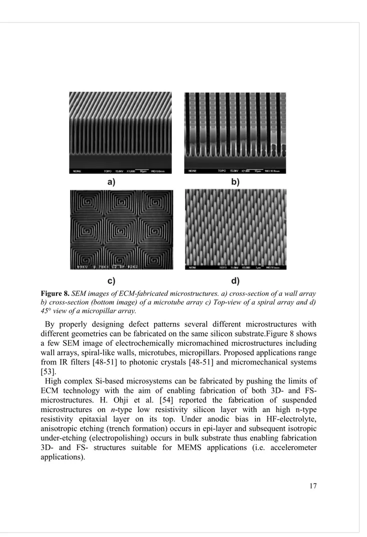
Figure 8. SEM images of ECM-fabricated microstructures. a) cross-section of a wall array b) cross-section (bottom image) of a microtube array c) Top-view of a spiral array and d) 45° view of a micropillar array.
By properly designing defect patterns several different microstructures with different geometries can be fabricated on the same silicon substrate.Figure 8 shows a few SEM image of electrochemically micromachined microstructures including wall arrays, spiral-like walls, microtubes, micropillars. Proposed applications range from IR filters [48-51] to photonic crystals [48-51] and micromechanical systems [53].
High complex Si-based microsystems can be fabricated by pushing the limits of ECM technology with the aim of enabling fabrication of both 3D- and FS- microstructures. H. Ohji et al. [54] reported the fabrication of suspended microstructures on n-type low resistivity silicon layer with an high n-type resistivity epitaxial layer on its top. Under anodic bias in HF-electrolyte, anisotropic etching (trench formation) occurs in epi-layer and subsequent isotropic under-etching (electropolishing) occurs in bulk substrate thus enabling fabrication 3D- and FS- structures suitable for MEMS applications (i.e. accelerometer applications).
Alternatively, bulk p-type layer with n-type epi-layer is used for fabrication of 3D- and FS-structures. In this case, after trenching of the epi-layer, the buried p-type layer is electropolished or converted in microporous materials that is used as sacrificial bulk layer. Microporous silicon can be easily removed by alkaline-based solutions to release micrormachined structures, thus yielding them freestanding [55]. In such approaches, with specific reference to the former, 3D and FS-microstructures are electrochemically fabricated exploiting a doping-based tunability of BIEE anisotropy.
Further improvement in ECM silicon microstructuring are obtained by amperometric tuning of BIEE anisotropy, which allows switching from anisotropic regime to isotropic. First use of amperometric-based tuning of BIEE anisotropy was reported by H. Ohji et al. [54]. In this works the authors provide a method for realising/making freestanding HAR (up to 25) microstructures exploiting enlargement of trenches at their bottom, which is produced by increasing etching current density while etching progresses. Particularly, width of trench is controlled by adjusting the light intensity. The process provides an initial anisotropic phase in which BIEE etching current density is controlled to produce vertical sidewall microstructures. After desired depth is obtained, etching current density is
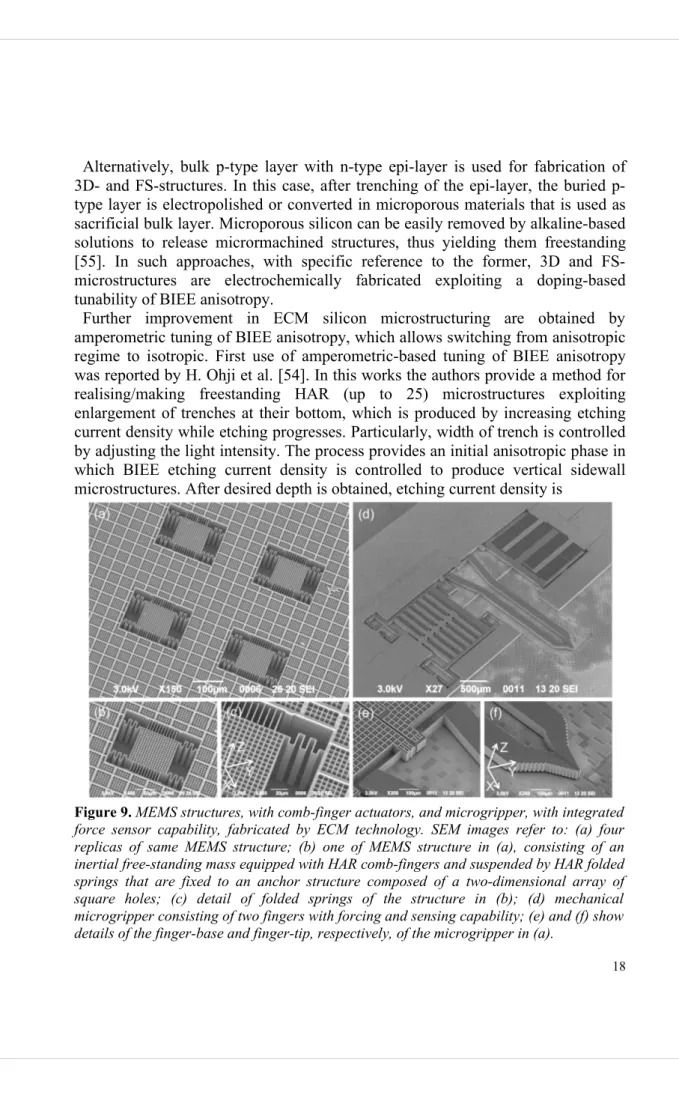
Figure 9. MEMS structures, with comb-finger actuators, and microgripper, with integrated force sensor capability, fabricated by ECM technology. SEM images refer to: (a) four replicas of same MEMS structure; (b) one of MEMS structure in (a), consisting of an inertial free-standing mass equipped with HAR comb-fingers and suspended by HAR folded springs that are fixed to an anchor structure composed of a two-dimensional array of square holes; (c) detail of folded springs of the structure in (b); (d) mechanical microgripper consisting of two fingers with forcing and sensing capability; (e) and (f) show details of the finger-base and finger-tip, respectively, of the microgripper in (a).
increased producing an enlargement of before micromachined trenches at their bottom. Underetching and in turn connection of trenches can be achieved and free standing structures are obtained with only one mask. Exploiting such approach, fabrication of suspended inertial mass for accelerometer applications was demonstrated. The inertial mass consists in a 500 × 1000 μm and 30 μm-thick perforated c-Si membrane supported by a single cantilever with a width of 4 μm and a length 500 μm.
Recently tunability of BIEE was successfully used in fabrication of 3D microstructures consisting in array of deep pore with both asymmetric (i.e. sawtooth-like current profile) and symmetric modulated diameter for fabrication of 3D silicon-based photonic crystal structures or micropumps for optical and microfluidic applications, respectively [55,56]. To achieve such a level of microfabrication complexity the authors used a mechanism for tuning BIEE anisotropy in which both voltage and current density are properly controlled.
More recently, ECM technology was further improved. In [53] the authors demonstrated that silicon microstructures of various shapes and silicon microsystems of high complexity can be effectively fabricated in any research lab with sub-micrometer accuracy and high aspect-ratio values (about 100). This is well beyond any up-to-date wet or dry microstructuring approach.
Dynamic control of the etching anisotropy (from 1 to 0) as the electrochemical etching progresses allows the silicon dissolution to be switched in real-time from the anisotropic to the isotropic regime and enables advanced silicon microstructuring to be achieved through the use of high-aspect-ratio functional and sacrificial structures, the former being functional to the microsystem operation and the latter being sacrificed for accurate microsystem fabrication. Figure 9 shows SEM images of as ECM-fabricated microstructures and microsystems. Figure 9(a) shows a SEM image of a MEMS structure consisting of an inertial, free-standing mass (340 μm × 340 μm × 130 μm) equipped with HAR comb-fingers and suspended by HAR folded springs (AR about 100) that are connected to an anchor structure composed of a 2D array of square holes; details at two different magnifications of the MEMS structure in panel (a) are shown in (b–c). Figure 9(d) shows SEM image of a mechanical microgripper consisting of two fingers (length of 1 mm and thickness of 70 μm), electrically actuable by means of comb-finger batteries driving a spring system, which allows rotation of the two fingers to be performed symmetrically (d); detail of the spring system exploited to allow symmetric rotation of the two microgripper fingers (e); and detail of one of the microgripper finger’s tip (f).
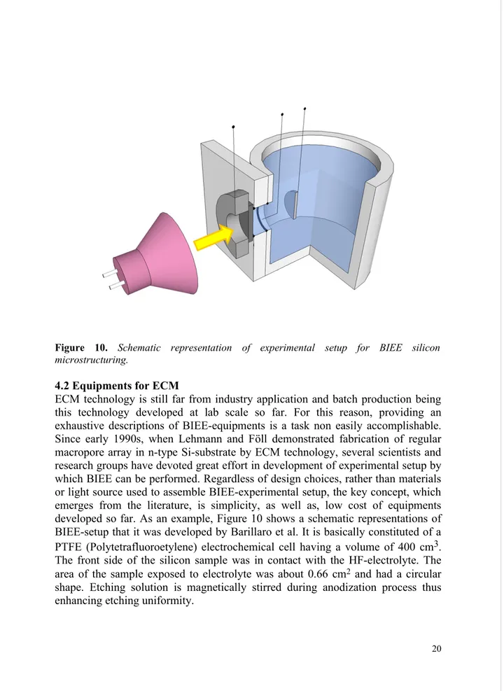
Figure 10. Schematic representation of experimental setup for BIEE silicon microstructuring.
4.2 Equipments for ECM
ECM technology is still far from industry application and batch production being this technology developed at lab scale so far. For this reason, providing an exhaustive descriptions of BIEE-equipments is a task non easily accomplishable. Since early 1990s, when Lehmann and Föll demonstrated fabrication of regular macropore array in n-type Si-substrate by ECM technology, several scientists and research groups have devoted great effort in development of experimental setup by which BIEE can be performed. Regardless of design choices, rather than materials or light source used to assemble BIEE-experimental setup, the key concept, which emerges from the literature, is simplicity, as well as, low cost of equipments developed so far. As an example, Figure 10 shows a schematic representations of BIEE-setup that it was developed by Barillaro et al. It is basically constituted of a PTFE (Polytetrafluoroetylene) electrochemical cell having a volume of 400 cm3. The front side of the silicon sample was in contact with the HF-electrolyte. The area of the sample exposed to electrolyte was about 0.66 cm2 and had a circular
shape. Etching solution is magnetically stirred during anodization process thus enhancing etching uniformity.
Back-side illumination of Si-sample is performed with a 250 W halogen lamp, through a circular window (0.66 cm2) in the metal electrode used to provide
electrical contact to the sample. A feedback loop, performed by using a PID controller (Eurotherm 2604), allows the lamp power, and thus illumination intensity, to be changed in order to proper set etching current density value as the etching progressed. An IR filter with a cutoff wavelength of 750 nm was placed between lamp and silicon sample in order to avoid carrier generation close to the silicon surface in contact with electrolyte. A second feedback loop, also obtained with the same PID controller, allows the working temperature to be maintained at 22 °C for the entire etching time. A platinum disc in front of silicon anode is used as cathode, whereas a platinum wire close to silicon electrode, at a distance of 2 mm, is used as a pseudo-reference electrode. A Source Measure Unit (Keithley 2410 Source Meter) is used to apply the anodization voltage, between silicon sample and reference electrode, and to monitor the etching current.
5.1 Laser Etching
Laser micromachining is a useful and versatile tool for rapid prototyping, small-scale production, and pre-form manufacturing. The principle of laser etching technology is that a laser beam modifies the surface (target) in which the beam is focused. The mechanism of laser etching is to irradiate the target with a localized high-energy radiation source (laser). The radiant energy is then absorbed by the material and converted to thermal energy. The thermal energy induces reactions to occur in the material. By scanning the laser beam (e.g. with movable mirrors), it is possible to define structures using a vector scan or a raster scan. Although lasers have been widely applied to process a variety of metallic materials, only few representative studies were reported to process silicon wafers for application in M(O)EMS.
One of the first works regarding this subject refers to Müllenborn and coworkers that in the 1995, studied laser micromachining of silicon for nanostructure fabrication. Only one year later, in 1996, Müllenborn et al. proposed a process based on argon lasers used to induce melting of silicon substrate in a chlorine atmosphere, thus enabling direct fabrication of 3D Si-microstructures with any arbitrary-shape and sub-micrometer accuracy. Particularly, the authors demonstrated as argon-based laser etching can be used in prototyping diffuser/nozzle element designed for a valve-less micropump, array of microlenses with area of 400μm × 400μm and a depth of 30μm [57].
Moreover, applying laser etching to 10-μm-thick silicon membrane, the authors demonstrated fabrication of suspended structures. However, argon lasers are not suitable for industrial applications, especially in IC and MEMES manufacturing process because of its power limitation. To overcame this limit excimer laserbased microstructuring for fabrication of ink jet nozzles holes with a diameter of 20μm
was demonstrated [58]. Alternatively to excimer laser-based mthod, C. Pan et al. [59] demonstrated that a 355 nm UV Nd:YAG laser can be successfully used to process silicon-based spiral microstructures with a high aspect ratio (up to 10). The major disadvantage of laser-machining techniques is that it leads to etched surface debris and wall damage due to recasting of molten material and the heat-affected zone. Very recently, M. Christophersen et al. [60] referred a laser micromaching method for fabrication of hole arrays into silicon substrate with aspect-ratio up to 100. Direct laser-drilling were used. Since laser-machining leaves a damaged silicon region the damaged silicon is removed with an isotropic xenon difluoride (XeF2) etch step.
Conclusions
Micromachining technologies based on state-of-the-art (e.g., cryogenic reactive ion etching) and commercial (e.g., wet and dry etching) approaches are reviewed by focusing on increased demand of high complexity microfabrication.
Wet anisotropic etching tools, allow high reproducibility, low cost and high smooth surfaces to be achieved, though reduced flexibility in designing Si-microsystems/microstructures. Dry etching tools allow HAR, high etching rate and both complexity and flexibility in microfabrication to be effectively achieved, though at higher cost.
A high level of complexity in silicon microstructuring can be easily achieved by combinig wet and dry etching with the use of SOI wafers. Significant improvement of DRIE-etched surfaces have been demonstrated by KOH post-processing (surface roughness reduced up to one order of magnitude). However, such approachs do not overcome all of the major drawbacks of both wet and dry technology, which are mainly related to reduced geometrical flexibility of feasible microstructures and to both ARDE effect and high roughness of sidewall surface, respectively. Moreover, high costs related to production of SOI wafers significantly limit crowning achievement of such technology to date.
Laser etching technology, seems to be very appealing microstructuring technology for new Si-HCMs prototyping, but is still so far form industry and batch production. Very appealing seems to be ECM technology, which combines advantages of both dry (high-flexibility) and wet (low-cost) standard silicon etching, thus representing today a unique case of straightforward, low-cost wet-etching technology with microfabrication flexibility typical of complex, high expensive dry-etching processes.
Reference
_________________________________________________________________ [1] Z. Fan, et al. Nat. Mater. 2009, 8, 648.
[2] G. M. Whitesides, Nature, 2006, 442, 368. [3] K. Sakuma et al, IBM J. Res. Dev., 2008, 52, 611.
[4] B. Wu, A. Kumar, S. Pamarthy, J. Appl. Phys. 2010, 108, 051101. [5] M. F. Aimi, et al., Nat. Mater. 2004, 3, 103.
[6] D. Copic, S. J. Park, S. Tawfi ck, M. F. L. De Volder, J. A. Hart, Lab Chip, 2011, 11, 1831.
[7] P. Rai-Choudhury, in MEMS and MOEMS technology and applications, SPIE Bellingham, Washington 2000.
[8] C. Liu, in Foundations of MEMS, Pearsonn Education, Inc, Upper Saddle River, New Jersey 2006.
[9] K. E. Bean, IEEE Transactions On Electron Device, 1978, 25(10), 1185.
[10] H. Seidel, L. Csepregi, A. Heuberger, H. Baumgärtel, J. Electrochem. Soc., 1990, 137(11), 3612.
[11] W. Lang, Mater. Sci. Eng., R, 1996, R17, I-55, and references within. [12] J. M. Bustillo, R. T. Howe, R. S. Muller, Proc. IEEE, 1998, 86(8), 1552. [13] M. Hoffmann, E. Voges, J. Micromech. Microeng., 2002, 12, 349. [14] M. Renilkumar, Prita Nair, Optical Materials, 2011, 33, 853.
[15] J. Haneveld, H. Jansen, E. Berenschot, N. Tas, M. Elwenspoek, J. Micromech. Microeng. 2003,13, S62.
[16] Z.Yang , H. Goto, M. Matsumoto, R. Maeda, Sensor Actuat. A, 2001, 93, 266.
[17] A. Chandrasekaran, A. Acharya, J. L. You, K. Y. Soo, M. Packirisamy, I. Stiharu, A. Darveau, Sensors, 2007, 7, 1901
[18] J. Ji, F.E.H. Tay, J. Miao, C. Iliescu, J. of Physics, 2006, 34, 1127.
[19] Garcia, E., Kirkham, J. R., Hatch, A.V, Hawkins, K.R. and Yager, P., Lab on a Chip, 2004, 4, 78.
[20] P. Pal, K. Sato, J. Micromech. Microeng., 2009, 19, 105008.
[22] M. Köhler , Etching in Microsystem Technology , Wiley-VCH , Weinheim-Germany 1999 , Ch. 3.
[23] B. Wu, A. Kumar, S. Pamarthy, J. Appl. Phys., 2010, 108, 051101, and references within.
[24] P. Abgrall, A-M Gué, J. Micromech. Microeng., 2007, 17, R15.
[25] M. Zimmermann, P. Hunziker, E. Delamarche, Microfluid. Nanofluid., 2008, 5, 395. [26] M. Zimmermann, H. Schmid, P. Hunziker, E. Delamarche, Lab Chip, 2007 7(1), 119. [27] N. Kockmann, T. Kiefer, M. Engler, P. Woias, Microfluid Nanofluid, 2006, 2, 327. [28] R. Huber, J. Conrad, L. Schmitt, K. Hecker, J. Scheurer, M. Weber, Microelectronic Engineering, 2003, 67–68, 410
[29] S.-S. Yun, S.-K. You, J.-H. Lee, Sens . Act . A. 2006, 128, 387;
[30] A. Lipson, E. M. Yeatman, J . Microelectromech . S . 2007 , 16(3), 521; [31] R. Mudachathi, P. Nair, J . Microelectromech . S . 2011 , in press. [32] www.oxford-instruments.com/plasma
[33] J. W. Kwon, E. S. Kim, Sensor Actuat. A, 2002, 97–98, 729.
[34] J.-P. Raskin, F. Ikera, N. André, B. Olbrechts, T. Pardoen, D. Flandre, Electrochimica Acta, 2007, 52, 2850.
[35] J.W. Graff , E.F. Schubert, Sensors and Actuators, 2000, 84, 276.
[36] M. Hoffmann, P. Kopka, T. Groß, E. Voges, J. Micromech. Microeng. 1999, 9, 151. [37] W. Noell, P.-A. Clerc, L. Dellmann, B. Guldimann, H. P. Herzig, O. Manzardo, C. Marxer, K. Weible, R Dändliker, N. de Rooij, JSTQE, 2002, 8(1), 148.
[38] S. E. Alper, K. Azgin, T. Akin, Sensors and Actuators A, 2007, 135, 34.
[39] B.E. Volland, H. Heerlein, I.W. Rangelow, Microelectronic Engineering, 2002, 61– 62 , 1015.
[40] J. Masson, R. St-Gelais, A. Poulin, Y.-A. Peter, IEEE JSTQE, 2010, 46(9), 1313. [41] M. Lutwyche,et al., Sensors and Actuators, 1999, 73, 89.
[42] B.H. Kima, D.P. Kerna, S. Raibleb, U. Weimarc, Microelectronic Engineering, 2002, 61–62, 947.
[43] P. Dumon et al. IEEE Photonics Technology Letters, 2004, 16(5), 1328 [44] V. Lehmann, H. Föll , J. Electrochem. Soc. 1990, 137, 653.
[45] V. Lehmann, J. Electrochem. Soc., 1993, 140, 2836.
[46] G. Barillaro, A. Diligenti, A. Nannini, G. Pennelli, Sens. Actuators, A Phys. 2003, 107, 279.
[47] G. Barillaro, F. D'angelo, G. Pennelli, F. Pieri, Physica Status Solidi A, Applications and Materials Science, 2005, 202 (8), 1427
[48] G. Barillaro, S. Merlo, L. Strambini, IEEE JSTQE, 2008, 14 (4), 1074.
[49] G. Barillaro, A. Diligenti, M. Benedetti, S. Merlo, Appl. Phys. Lett., 2006, 89 (15),151110/1.
[50] G. Barillaro, V. Annovazzi-Lodi, M. Benedetti, S. Merlo, Appl. Phys. Lett. 2007,90(12), 121110/1.
[51] G. Barillaro, L. M. Strambini, V. Annovazzi-Lodi, S. Merlo, IEEE JSTQE, 2009, 15(5); 1359.
[52] G. Barillaro, A. Nannini, M. Piotto, Physica Status Solidi. A, Applications and Materials Science, 2007, 204 (5), 1464.
[53] M. Bassu, S. Surdo, L. M. Strambini, G. Barillaro, Adv. Funct. Mat. 2012, DOI: 10.1002/adfm.201102124.
[54] H. Ohji, P. J. Trimp, P. J. French, Sens. Actuators A, 1999, 73, 95, and references within.
[55] S. Matthias , F. Müller , Nature, 2003, 424, 53.
[56] T. Trifonov, et al., Sensors and Actuators A, 2008, 141, 662, and references within. [57] M. Mtillenborn et al., Sensors and Actuators A, 1996, 52, 121.
[58] Y. Zhang, Appl. Surf. Sci., 2002, 186, 345. [59] C.T. Pan, Sensors and Actuators A, 2005, 122, 45.
[60] M. Christophersen, B. F. Phlips, IEEE Nuclear Science Symposium Conference Record (NSS/MIC), 2010 , 10.1109/NSSMIC.2010.5873784
![Figure 4. SEM micrograph of free-standing crystalline silicon cantilever structure with integrated V-groove [35].](https://thumb-eu.123doks.com/thumbv2/123dokorg/7612426.115404/6.892.82.812.74.1162/figure-micrograph-standing-crystalline-silicon-cantilever-structure-integrated.webp)
![Figure 6. Four-level silicon structures fabricated by SHALLOW process, (a) four-level microfluidic devices and 3-D gear wheel (b) [28].](https://thumb-eu.123doks.com/thumbv2/123dokorg/7612426.115404/12.892.87.805.90.1148/figure-silicon-structures-fabricated-shallow-process-microfluidic-devices.webp)