CHAPTER 6
Optofluidic Microsystems with Integrated Vertical One-Dimensional
Photonic Crystals for Chemical Analysis
Abstract
In this work, for the first time, we report the successful application of the electrochemical micromachining (ECM) technology to the realization of all-silicon optofluidic microsystems (OFMs) in which high aspect-ratio (HAR) photonic crystal (PhC) devices (i.e. micromirrors, optical cavities) are integrated by one-etching-step together with microfluidic reservoirs/channels, for the infiltration of liquids in the PhC air gaps, as well as fiber grooves, for alignment/positioning of readout optical fibers in front of the PhC, on the same silicon die. Fabrication of PhC-OFMs by ECM technology is performed by exploiting a dynamic control of the etching anisotropy as the electrochemical etching progresses, which allows the silicon dissolution to be switched in real-time from the anisotropic to the isotropic regime and enables advanced silicon microstructuring to be carried out through the use of both functional and sacrificial structures, with sub-micrometric accuracy at aspect-ratio values not attainable by up-to-date wet and dry microstructuring technologies. Optofluidic characterization of PhC-OFMs by both capillary-action and pressure-driven operation is carried out through the measurement of the reflectivity spectra of HAR-PhCs upon injection of liquids featuring different refractive index values in the HAR-PhC air gaps, by using readout optical fibers positioned in the on-chip fiber grooves. High sensitivity and good limit of detection of PhC-OFMs are obtained both for capillary-action and pressure-driven operation. A best sensitivity value of 670 nm/RIU and best limit of detection of the order of 10-3 are measured, the former being comparable to state-of-the-art integrated refractive index sensors and the latter being limited by constraints of the experimental setup.
Keywords: photonic crystals, label-free, optofluidic microsystem, electrochemical micromachining, chemical analysis
1 Introduction
There is an increasing research trend in the fabrication of a novel generation of optofluidic microsystems (OFMs) for label-free biological/chemical analysis that integrate materials with unique optical properties, among which photonic crystals, in microfluidic systems [1-4].
Photonic crystals (PhCs) are artificial or natural micro/nano-structures characterized by spatial, periodic arrangement of dielectric materials with sufficiently high refractive index contrast in one (1D), two (2D), or three (3D) dimensions [5,6]. PhCs have been a subject of great interest in the material science community, since many years to now, thanks to their unique characteristic of featuring a photonic bandgap (PBG) that allows manipulation of light propagation at sub-wavelength scale to be effectively performed [7-10]. PhCs have been successfully used for a broad range of applications, from optoelectronics [11] to photocatalysys [12], from photovoltaics [12] to displays [13]. More recently, PhCs have attracted great attention in the field of biological/chemical analysis for the realization of label-free sensors that exploits the high sensitivity of PhC optical properties to tiny changes of the dielectric constant and/or thickness of the composing materials upon interaction of the PhC with the analyte/fluid to be identified [2,14]. Integration of such PhC structures into microfluidic networks has lead to the first generation of PhC optofluidic microsystems (PhC-OFMs)[1, 15-17], in which planar PhCs characterized by a reduced value of the aspect-ratio (height-to-width ratio smaller than or about 1) are employed to monitor changes of PhC optical properties induced by light-matter interaction of analytes/fluids with the PhC structure at surface level. High sensitivity and low limit of detection have been experimentally demonstrated for such a first generation of label-free PhC-OFMs for both biological and chemical analyses. However, though a number of different architectures have been proposed for increasing light-matter interaction at the PhC surface, performances of planar PhC-OFMs are often limited by the inefficient "flow over" technique employed for analyte/fluid transport, instead of PhC intrinsic detection capabilities; on the one hand, the microfluidic system is often unable to selectively deliver analytes where light-matter interaction is strongest, so limiting sensitivity values; on the other hand, the microfluidic system is ineffective in transporting a large number of molecules to the PhC sensing surface due to slow diffusion kinetic processes, which at slow concentrations causes impractically long detection times, so increasing limit of detection values. Very recently, besides planar PhC structures, vertical PhC structures with high aspect-ratio (greater than 1) obtained by periodic arrangement of air voids in dielectric materials, e.g. silicon, have been proposed for the fabrication of a second generation of PhC-OFMs, in which the "flow over" technique is replaced with a "flow-through" strategy, throughout the PhC structure-itself, that exploits air voids as micro/nano-channels for fluid flow [18-20]. The flow-through strategy allows
excellent sensitivity and limit of detection to be achieved, while simultaneously reducing detection times with respect to the flow-over technique, both for biological and chemical analyses [21-22]. Mass transport is almost entirely convective, instead of diffusive, which provides a stronger signal in significantly less time than the conventional flow-over approach, for both surface and bulk refractive index detection. As to surface refraction index detection, surface-to-volume ratio is largely increased thus enabling adsorption/linking of a larger number of molecules on the PhC surface. As to bulk refraction index detection, light-matter interaction is moved from surface to bulk thus enabling deeper interaction between light and fluid. Reflection from multiple periodic surfaces, instead of reflection from a single surface, as it usually happens in planar PhC structures, allows higher signal-to-noise ratios to be achieved both for surface and bulk refraction index detection. Furthermore, such a second generation of PhC-OFMs features fluidic and optical paths that are inherently independent, being the former through the air voids and the latter perpendicular to the air voids. This enables integration of both fluidic and optical sections on the same chip as the PhC transducer, which is straightforward for 1DPhCs, thus envisioning a novel generation of optical lab-on-chip with advanced on-chip fluidics (sample preparation, liquid mixing, etc.) and optical (signal routing and elaboration, signal multiplexing, etc.) features.
An analysis of the literature of high aspect-ratio (HAR) PhCs for optofluidic applications points out that the second generation of PhC-OFMs is very promising for both biological and chemical applications, though still in its infancy. A few interesting cases of vertical HAR-1DPhC structures integrated into optofluidic microsystems by using dry etching technology, namely Deep Reactive Ion Etching (DRIE) [18, 19], or wet etching technology have been reported in the literature so far [20]. Nunes et al. [18] reported the integration of vertical silicon-dioxide/air 1DPhCs with AR about 3, fabricated by trenching a 9-µm-thick silicon dioxide layer, together with microfluidic channels and waveguides on the same chip. A best sensitivity value of 836 nm/RIU at 1.55 μm and limit of detection of 6x10⁻⁵ RIU (Refractive Index Unit) are claimed for such a microsystem [23], the former being comparable to sensitivities of state-of-the-art planar PhC structures [16]. St-Gelais et al.[19] reported the integration of vertical Fabry-Perot cavities that exploit silicon/air 1DPhC micromirrors with AR about 35, together with microfluidic channels and fiber grooves on the same silicon die. A sensitivity value of 907 nm/RIU at 1.55 μm and a resolution of 1.7x10⁻⁵ RIU are obtained, the latter claimed by authors to be the highest reported for volume refractive index sensors integrated with microfluidic channels [24]. Barillaro et al. [20] reported vertical HAR-1DPhC micromirrors integrated into optofluidic microsystems by using silicon wet etching technology. The 1D PhC micromirrors, with AR about 40, were fabricated by electrochemical micromachining (ECM) of silicon and integrated on the same chip together with fluidic microchannels obtained by potasium hydroxide
(KOH) etching. A sensitivity value of 1049 nm/RIU at 1.55 μm and limit of detection of 10-3 RIU are obtained, the former being comparable to sensitivities of state-of-the-art integrated refractive index sensors [25].
The fabrication of optofluidic microsystems exploiting HAR-PhCs is undoubtedly more challenging than that of optofluidic microsystems exploiting planar PhCs, the former requiring the use of advanced microstructuring technologies that allow in-plane silicon dissolution to be finely controlled both over small (e.g. a few micrometers) and large areas (e.g. thousands of micrometers) up to tens of microns in the out-of-plane direction (as opposed to a few tens nanometers of planar PhC-OFMs). On the one hand, dry etching technologies, e.g. DRIE, allow high flexibility in microfabrication with respect to wet etching technology, at higher cost, though they are affected by drawbacks in the out-of-plane direction (e.g. limited aspect-ratio, deviation from the verticality, lag-etching of small and large areas, scalloping of etched surfaces, etc. [26]) that reduce the optical quality of fabricated photonic structures [27]; on the other hand, anisotropic wet etching technologies, e.g. KOH, allow vertical silicon microstructures with excellent surface flatness to be fabricated on (110)-oriented substrates [28], at lower cost, though with significantly reduced flexibility and aspect-ratio with respect to dry etching technologies, due to the crystalline-orientation dependent etching rate [29]. In order to enable high flexibility in microfabrication and etching of high quality vertical surfaces, dry (e.g. DRIE) and wet (e.g. KOH) etchings have been combined for the realization of optical microsystems for telecommunication applications, in which DRIE-etched microsystems with high aspect-ratio are post-processed by KOH etching to improve surface quality of optical structures [30-32]. Though significant improvement of the quality of DRIE-etched surfaces have been demonstrated by KOH post-processing (surface roughness reduced up to one order of magnitude), others drawbacks of dry etching technologies in the out-of-plane direction (e.g. deviation from verticality, lag-etching problems, etc.) are not easily addressable with the same approach. Summarizing, on the one hand, technological problems of both dry and wet technologies connected with the etching of HAR complex microsystems for optical applications can be only partially solved by the combination of wet and dry technologies; on the other hand, it increases fabrication costs with respect to both dry and wet technologies.
More recently, advanced fabrication of complex silicon microstructures (e.g. comb-drive actuators, folded springs) and microsystems (e.g. MEMS, microgrippers) with sub-micrometer accuracy at aspect-ratio values (about 100) well beyond dry etching technologies has been proven to be feasible in any research lab by using a wet etching, low cost technology, namely the ECM technology [33]. ECM technology have been to date successfully used for the fabrication of vertical (up to 100 μm deep) 1DPhCs with elevated optical quality (i.e. deviation from the verticality of about 0.02° and roughness of etched surfaces
of about 20 nm for 100-μm-deep structures) at high aspect-ratio values (over 50), which is beyond up-to-date dry and wet technologies [20-34-36].
In this work, for the first time, we report the successfully application of the ECM technology to the realization of all-silicon HAR PhC-OFMs. In particular, we detail and discuss design and fabrication, by ECM technology, as well as optofluidic characterization, by both capillary action and pressure-driven operation, of ECM-fabricated all-silicon HAR PhC-OFMs, in which HAR-PhC devices (i.e. micromirrors, optical cavities) are integrated by one-etching-step together with microfluidic reservoirs/channels, for the infiltration of liquids in the PhC air gaps, as well as fiber grooves, for alignment/positioning of readout fibers in front of the PhC for its optical characterization, on the same silicon die. Fabrication of PhC-OFMs by ECM technology is performed by exploiting a dynamic control of the etching anisotropy as the electrochemical etching progresses, which allows the silicon dissolution to be switched in real-time from the anisotropic to the isotropic regime and enables advanced silicon microstructuring through the use of high aspect-ratio functional and sacrificial structures, the former being functional to the microsystem operation and the latter being sacrificed for the accurate microsystem fabrication. Optofluidic characterization of PhC-OFMs is carried out by measuring the reflectivity spectra of HAR-PhCs upon injection of liquids featuring different refractive index values in the HAR-PhC air gaps, by using readout optical fibers positioned in the on-chip fiber grooves. A best sensitivity value of 670 nm/RIU and limit of detection of about 10-3 are obtained, the former being comparable to state-of-the-art integrated refractive index sensors and the latter being limited by the spectral resolution and thermal/amplitude noise of the measurement setup. This work clearly assesses ECM technology as a effective tool for low-cost, advanced silicon microstructuring in any lab.
2. PhC-OFM Design and Fabrication
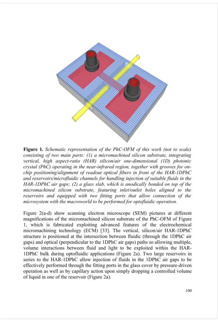
Photonic crystal optofluidic microsystems (PhC-OFMs) consist of two main parts: (1) a micromachined silicon substrate, integrating vertical, high aspect-ratio (HAR) silicon/air one-dimensional (1D) photonic crystals (PhCs) operating in the near-infrared region, together with grooves for on-chip positioning/alignment of readout optical fibers in front of the HAR-1DPhC and reservoirs/microfluidic channels for handling injection of suitable fluids in the HAR-1DPhC air gaps; (2) a glass slab, which is anodically bonded on top of the micromachined silicon substrate, featuring inlet/outlet holes aligned to the reservoirs and equipped with two fitting ports that allow connection of the microsystem with the macroworld to be performed for pressure-driven optofluidic operation. A schematic representation of the PhC-OFM of this work is shown in Figure 1 (not to scale).
Figure 1. Schematic representation of the PhC-OFM of this work (not to scale)
consisting of two main parts: (1) a micromachined silicon substrate, integrating vertical, high aspect-ratio (HAR) silicon/air one-dimensional (1D) photonic crystal (PhC) operating in the near-infrared region, together with grooves for on-chip positioning/alignment of readout optical fibers in front of the HAR-1DPhC and reservoirs/microfluidic channels for handling injection of suitable fluids in the HAR-1DPhC air gaps; (2) a glass slab, which is anodically bonded on top of the micromachined silicon substrate, featuring inlet/outlet holes aligned to the reservoirs and equipped with two fitting ports that allow connection of the microsystem with the macroworld to be performed for optofluidic operation.
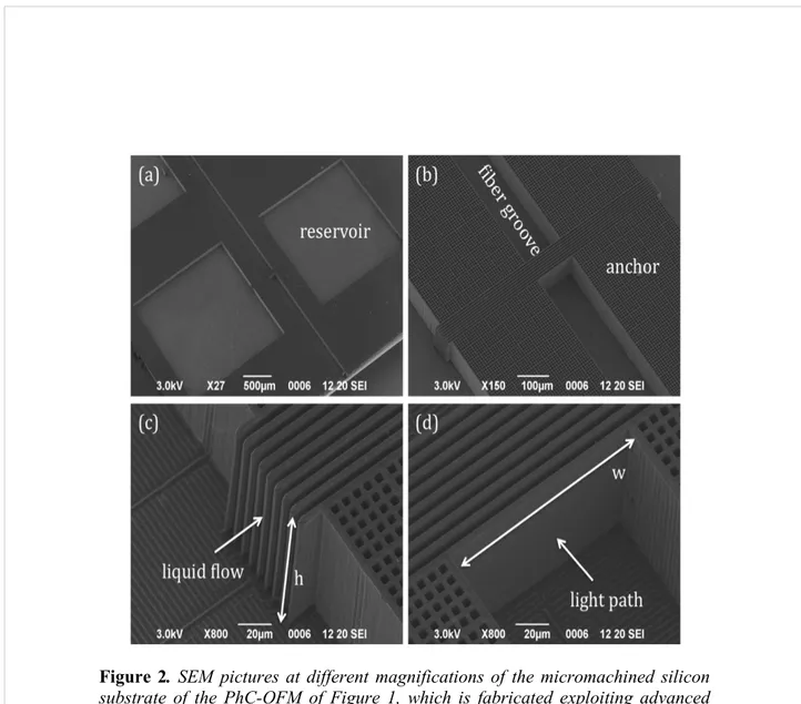
Figure 2(a-d) show scanning electron microscope (SEM) pictures at different magnifications of the micromachined silicon substrate of the PhC-OFM of Figure 1, which is fabricated exploiting advanced features of the electrochemical micromachining technology (ECM) [33]. The vertical, silicon/air HAR-1DPhC structure is positioned at the intersection between fluidic (through the 1DPhC air gaps) and optical (perpendicular to the 1DPhC air gaps) paths so allowing multiple, volume interactions between fluid and light to be exploited within the HAR-1DPhC bulk during optofluidic applications (Figure 2a). Two large reservoirs in series to the HAR-1DPhC allow injection of fluids in the 1DPhC air gaps to be effectively performed through the fitting ports in the glass cover by pressure-driven operation as well as by capillary action upon simply dropping a controlled volume of liquid in one of the reservoir (Figure 2a).
Figure 2. SEM pictures at different magnifications of the micromachined silicon
substrate of the PhC-OFM of Figure 1, which is fabricated exploiting advanced features of the electrochemical micromachining technology (ECM). (a) Bird view of the whole PhC-OFM. The two large reservoirs connecting the 1DPhC are clearly visible. (b) Magnification of (a) showing the core of the PhC-OFM. The PhC structure is clearly visible at the intersection of optical and fluidic paths. Fiber grooves and anchor structure are also highlighted. (c) Magnification of (b) showing the fluidic inlet section of the HAR-1DPhC. (d) Magnification of (b) highlighting the microstructure of the HAR-1DPhC.
Fiber grooves (Figure 2b) allow fine positioning/alignment of readout optical fibers in front of the 1DPhC to be achieved and, in turn, in-plane reflection (and/or transmission) measurements with/without liquids flowing in the HAR-1DPhC to be accomplished with high repeatability/accuracy. The anchor structure (Figure 2a and 2b) allows mechanical stability of the PhC-OFM to be ensured as well as leakage of liquid into the fiber grooves during optofluidic operation of the
microsystem to be avoided. Details of both the microfluidic inlet section of the 1DPhC and 1DPhC three-dimensional silicon microstructure are shown in Figure 2c and 2d, respectively, which allow the high accuracy in microfabrication of complex microsystems featuring HAR structures as well as the high quality of surfaces that are achievable by means of the electrochemical micromachining (ECM) technology to be clearly appreciated.
The core element of the proposed PhC-OFM is a vertical, silicon/air HAR-1DPhC micromirror featuring a number of high-order bandgaps with high-reflectivity in the near-infrared region (1.0-1.7 μm), among which one centered around the operation wavelength λ=1.55 μm. Design of the 1DPhC micromirror is analytically performed according to the so-called hybrid quarter-wavelength stack [37], which consists of an array of silicon layers with thickness dSi and air gaps of width dAir satisfying the conditions dSi = Mλ/4nSi and dAir = Nλ/4, where M and N are odd integer, independent parameters, nSi is the silicon refractive index at λ (whereas air refractive index is 1), and n=(M+N)/2 is the order of the n-th bandgap, which is centred at λ. Design parameters at the operation wavelength λ=1.55 μm are the silicon refractive index nSi=3.48, the spatial period p= dSi+dAir=8 μm, and the porosity of the structure D= dAir/p=0.62, which gives rise to silicon walls with thickness dSi = 3.04 μm (M=27) and air gaps with width dAir= 4.96 μm (N= 13) and, in turn, to a high-order bandgap (namely the 20th) centered at λ=1.55 μm. Both period p and porosity D, and, in turn, the thickness of silicon layers dSi are chosen to obtain a mechanically robust silicon/air HAR-1DPhC able to withstand liquid insertion/extraction in/from the air gaps during optofluidic applications, specially for capillary action operation that is performed on the silicon microsystem without cover on top. Height h and width w of the 1DPhC active section and, in turn, of the fiber grooves are set to 100 μm and 130 μm, respectively, in order to comply with the diameter of readout optical fibers. The height h of the 1DPhC also defines the height of any other structure etched on the same silicon chip. The size of the reservoirs is set to about 2000 μm x 2000 μm in order to comply with the fitting ports internal/external diameter, which is 1.2/1.5 mm in this work.
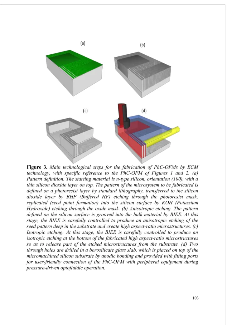
Fabrication of PhC-OFMs by ECM technology is carried out according to the following main technological steps, which are sketched in Figure 3 with specific reference to the microsystem of Figures 1 and 2. The starting material is n-type silicon, orientation (100), with a thin silicon dioxide layer on top. The pattern of the microsystem to be fabricated is defined on a photoresist layer by standard lithography, transferred to the silicon dioxide layer by Buffered HF (BHF) etching through the photoresist mask, replicated (seed point formation) into the silicon surface by Potassium Hydroxide (KOH) etching through the oxide mask (Figure 3a), and finally grooved into the bulk material by back-side illumination electrochemical etching (BIEE).
Figure 3. Main technological steps for the fabrication of PhC-OFMs by ECM
technology, with specific reference to the PhC-OFM of Figures 1 and 2. (a) Pattern definition. The starting material is n-type silicon, orientation (100), with a thin silicon dioxide layer on top. The pattern of the microsystem to be fabricated is defined on a photoresist layer by standard lithography, transferred to the silicon dioxide layer by BHF (Buffered HF) etching through the photoresist mask, replicated (seed point formation) into the silicon surface by KOH (Potassium Hydroxide) etching through the oxide mask. (b) Anisotropic etching. The pattern defined on the silicon surface is grooved into the bulk material by BIEE. At this stage, the BIEE is carefully controlled to produce an anisotropic etching of the seed pattern deep in the substrate and create high aspect-ratio microstructures. (c) Isotropic etching. At this stage, the BIEE is carefully controlled to produce an isotropic etching at the bottom of the fabricated high aspect-ratio microstructures so as to release part of the etched microstructures from the substrate. (d) Two through holes are drilled in a borosilicate glass slab, which is placed on top of the micromachined silicon substrate by anodic bonding and provided with fitting ports for user-friendly connection of the PhC-OFM with peripheral equipment during pressure-driven optofluidic operation.
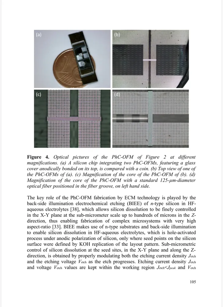
The BIEE consists of a single-etching-step with an initial anisotropic phase (Figure 3b), used to etch the seed pattern deep in the substrate and create high aspect-ratio microstructures, and a final isotropic phase (Figure 3c), used to release sacrificial structures from the substrate while leaving functional structures anchored to it. Two through holes are drilled in a borosilicate glass slab, which is placed on top of the micromachined silicon substrate by anodic bonding and provided with fitting ports for connection of the PhC-OFM with peripheral equipment during pressure-driven optofluidic operation (Figure 3d). Figure 4 shows optical pictures of the PhC-OFM of Figure 2 at different magnifications (Figure 4a-4c); in Figure 4d the PhC-OFM is shown with a standard readout optical fiber positioned in the fiber groove. As schematically shown in Figure 3, ECM makes use of both functional and sacrificial structures for fabrication of advanced silicon microsystems [33]. Functional structures are, by definition, parts of the microsystem that are anchored (partially, at least) to the silicon substrate after the isotropic phase of the electrochemical etching step. Sacrificial structures are, by definition, parts that are not anchored to the silicon substrate after the isotropic phase of the electrochemical etching step and are, hence, removed. The former are indeed functional to the microsystem operation, while the latter are sacrificed for the accurate microsystem fabrication.
All the microsystem parts visible in the SEM pictures of Figure 2 are functional structures that were properly designed to withstand the isotropic phase of the etching and are still connected to the substrate at either their bottom or through suitable anchor structures; sacrificial structures in Figure 2 are no more visible as they were designed to be effectively removed during the isotropic phase of the electrochemical etching step in order to produce fiber grooves as well as reservoirs. Figures 2c and 2d clearly show the effect of the isotropic phase of the electrochemical etching step on both functional and sacrificial structures: the HAR-1DPhC is anchored to the silicon substrate after the isotropic phase, while sacrificial structures around both 1DPhC and anchor structures are removed after the isotropic phase leaving a characteristic ripple on the bottom surface. The use of sacrificial structures allows the simultaneous etching of both small (feature of a few microns) and large (length of several millimeters) area to be performed at the same rate and with the same accuracy, so eliminating lag-effect problems on silicon areas with different aspect-ratio, which is a major problem of dry etching technologies. In addition, fabrication of structures featuring a reduced aspect-ratio value, such as reservoirs, fluidic microchannels, and fiber grooves, are fabricated with the same accuracy of structures featuring a high aspect-ratio value, such as 1DPhC and anchor structures, by just exploiting one-etching-step.
Figure 4. Optical pictures of the PhC-OFM of Figure 2 at different
magnifications. (a) A silicon chip integrating two PhC-OFMs, featuring a glass cover anodically bonded on its top, is compared with a coin. (b) Top view of one of the PhC-OFMs of (a). (c) Magnification of the core of the PhC-OFM of (b). (d) Magnification of the core of the PhC-OFM with a standard 125-µm-diameter optical fiber positioned in the fiber groove, on left hand side.
The key role of the PhC-OFM fabrication by ECM technology is played by the back-side illumination electrochemical etching (BIEE) of n-type silicon in HF-aqueous electrolytes [38], which allows silicon dissolution to be finely controlled in the X-Y plane at the sub-micrometer scale up to hundreds of microns in the Z-direction, thus enabling fabrication of complex microsystems with very high aspect-ratio [33]. BIEE makes use of n-type substrates and back-side illumination to enable silicon dissolution in HF-aqueous electrolytes, which is hole-activated process under anodic polarization of silicon, only where seed points on the silicon surface were defined by KOH replication of the layout pattern. Sub-micrometric control of silicon dissolution at the seed sites, in the X-Y plane and along the Z-direction, is obtained by properly modulating both the etching current density Jetch and the etching voltage Vetch as the etch progresses. Etching current density Jetch and voltage Vetch values are kept within the working region Jetch<Jpeak and Vetch
>Vpeak (Figure S1 supporting material), where Jpeak and Vpeak represent current density and voltage values, respectively, of the electropolishing peak of the electrochemical system under investigation for flat silicon electrodes. In the working region, silicon mass dissolved per unit time around a given X-Y position is proportional to the ratio Jetch/Jpeak (also known as porosity D) for any etching depth; the Jpeak value also determines the etching rate in the Z-direction, which is indeed proportional to Jpeak.
Silicon dissolution (in terms of both volume and isotropy versus time) is finely tuned as the etching progresses by properly controlling the Jetch value over time, while the value of Vetch is kept constant (Figure S1 supporting material). Although a better control of the etching process is achieved by modulating the etching voltage value Vetch over time [33], good results in microfabrication are obtained at constant
Vetch for etching depth up to 100 μm. As to the etching current density, on one hand, if the Jetch value is slowly reduced over time according to HF diffusion kinetics, it is possible to compensate for the slight reduction of the Jpeak value with the etching depth, so that by maintaining the Jetch/Jpeak ratio constant over time the etching results to be perfectly anisotropic and micromachined structures with excellent straight walls are achieved. The reduction of Jpeak with the etching depth is caused by the reduction of the HF concentration (CHF) inside the etched trenches with respect to the bulk electrolyte HF concentration, due to stationary diffusion of HF molecules from top to bottom of etched structures. The continuous compensation of Jetch with time over the whole etching depth allows deviation from verticality of etched structures to be significantly reduced with respect to dry etching technology, as well as to avoid periodic surface scalloping effects. On the other hand, if the Jetch value is suddenly increased over time with respect to HF diffusion kinetics, a dramatic decrease of the Jpeak value occurs that dynamically increases the Jetch/Jpeak ratio, and in turn the silicon mass dissolved per unit time. A higher number of HF molecules per unit time, with respect to that supplied by stationary diffusion, are consumed at the bottom of etched trenches as a consequence of sudden increase of the Jetch value. The excess of HF molecule consumption leads to a dynamic reduction of the CHF value and, in turn, of the Jpeak value at the bottom of etched trenches. The etching rate in the Z-direction being proportional to Jpeak is therefore reduced, and the increased mass of silicon removed per unit time Jetch/Jpeak mainly occurs in the X and Y directions, thus switching the etching from anisotropic to isotropic (see Ref. [33] for details).
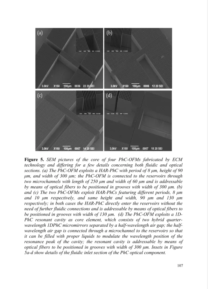
Figure 5. SEM pictures of the core of four PhC-OFMs fabricated by ECM
technology and differing for a few details concerning both fluidic and optical sections. (a) The PhC-OFM exploits a HAR-PhC with period of 8 μm, height of 90 μm, and width of 300 μm; the PhC-OFM is connected to the reservoirs through two microchannels with length of 250 μm and width of 60 μm and is addressable by means of optical fibers to be positioned in grooves with width of 300 μm. (b) and (c) The two PhC-OFMs exploit HAR-PhCs featuring different periods, 8 μm and 10 μm respectively, and same height and width, 90 μm and 130 μm respectively; in both cases the HAR-PhC directly enter the reservoirs without the need of further fluidic connections and is addressable by means of optical fibers to be positioned in grooves with width of 130 μm. (d) The PhC-OFM exploits a 1D-PhC resonant cavity as core element, which consists of two hybrid quarter-wavelength 1DPhC micromirrors separated by a quarter-wavelength air gap; the half-wavelength air gap is connected through a microchannel to the reservoirs so that it can be filled with proper liquids to modulate the wavelength position of the resonance peak of the cavity; the resonant cavity is addressable by means of optical fibers to be positioned in grooves with width of 300 μm. Insets in Figure 5a-d show details of the fluidic inlet section of the PhC optical component.
Despite the fabrication process is here detailed for the specific case of the PhC-OFM of Figure 2, optofluidic microsystems differing for both fluidic and optical sections can be effectively produced by using the ECM technology after a proper design of the microsystem layout has been defined. Figure 5 shows SEM pictures of the core of four PhC-OFMs differing for a few details concerning both fluidic and optical sections. In Figure 5a, the PhC-OFM exploits a HAR-PhC with period of 8 μm, height of 100 μm, and width of 300 μm; the PhC-OFM is connected to the reservoirs through two microchannels with length of 250 μm and width of 60 μm and is addressable by means of optical fibers to be positioned in grooves with width of 300 μm. In Figure 5b and 5c, the two PhC-OFMs exploit HAR-PhCs featuring different periods, 8 μm and 10 μm respectively, and same height and width, 100 μm and 130 μm, respectively; in both cases the HAR-PhC directly enter the reservoirs without the need of further fluidic connections and is addressable by means of optical fibers to be positioned in grooves with width of 130 μm. In Figure 5d, the PhC-OFM exploits a 1D-PhC resonant cavity as core element, which consists of two hybrid quarter-wavelength 1DPhC micromirrors separated by a half-wavelength air gap; the half-wavelength air gap is connected through a microchannel to the reservoirs so that it can be filled with proper liquids in order to modulate the wavelength position of the resonance peak of the cavity; the resonant cavity is addressable by means of optical fibers to be positioned in grooves with width of 300 μm. Insets in Figure 5a-d show details of the fluidic inlet section of the PhC optical component.
3. PhC-OFM Operation and Characterization
Optofluidic characterization of PhC-OFMs is carried out injecting liquids (water, ethanol, isopropanol, and water/ethanol mixtures [39]) with different refractive index values in the HAR-PhC air gaps by both capillary-action and pressure-driven operation. Experimental measurement of the optical power reflected from HAR-PhCs upon liquid injection is performed using optical fibers positioned into the fiber groove in front of the PhC-itself (see Figure 4d). For each tested liquid, measurement of the reflected power spectrum is performed before infiltration of the PhC with the liquid (empty microsystem), after infiltration of the liquid in the air gaps of the PhC (filled microsystem), and after removal of the liquid from the PhC air gaps (empty microsystem). The procedure is repeated several times for each tested liquid so as to investigate both repeatability and accuracy of the PhC-OFM operation for optofluidic applications. Optical measurements were performed at room temperature, without the use of a feedback loop for temperature monitoring/control. After acquisition, experimental power spectra are low-pass filtered in the Fourier Transform domain in order to increase the signal-to-noise ratio and, in turn, to reduce the effect of measurement noise on the peak position, then the position of the different reflectivity peaks is automatically detected.
Reflected power spectra are then normalized with respect to an ideal reflector by numerical elaboration using, as reference, the glass-air interface at the output connector [35].
3.1. Capillary action operation
Capillary-action operation is investigated using three different liquids, namely water, ethanol, and isopropanol, which readily infiltrate the HAR-PhC air gaps by capillary action after a calibrated volume (0.5 μl) of the liquid substance is dropped into one of the reservoirs of the silicon microsystem, in this case without any cover on top. The liquid quickly expands from the reservoir to the PhC structure, uniformly filling the air gaps and producing a dramatic change in the reflectivity spectrum of the HAR-PhC with respect to the reference spectrum in air. The remarkable change in the line-shape of the reflectivity spectrum of the PhC structure is due to the significant increase of the effective refractive index of the photonic material upon replacement of air with liquids, which gives rise to higher order bandgaps to appear in the wavelength range under observation (compare Figure 6a to Figure 6b-6d). The change in the line-shape does not significantly depend on the specific liquid infiltrated in the HAR-PhC, as the relatively small variation of the refractive index between the different liquids investigated in this work does not produce any further change in the order of bandgaps in the wavelength range under observation. However, the slight increase of the refractive index value from water to ethanol and isopropanol produces a reliable shift of the reflectivity spectrum toward longer wavelengths [40]. The magnitude of the shift correlates well with the refractive index value of the substance infiltrated in the PhC structure. After the gaps are filled, the liquid starts evaporating from the PhC air gaps with a characteristic time that decreases as the surface tension of the liquid increases (from water, to ethanol, and isopropanol), thus rapidly bringing the reflectivity spectrum back to the reference spectrum in air.
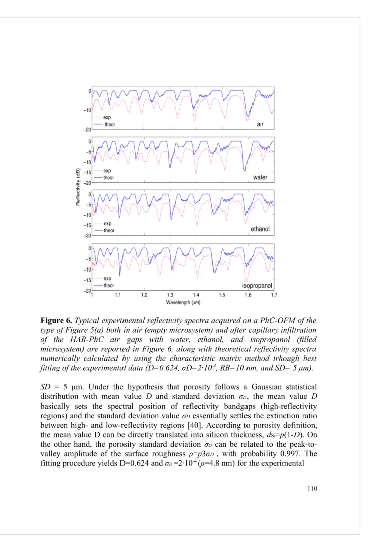
Typical experimental reflectivity spectra acquired on a PhC-OFM of the type of Figure 5a both in air (empty microsystem) and after capillary infiltration of the HAR-PhC air gaps with water, ethanol, and isopropanol (filled microsystem) are reported in Figure 6, along with theoretical reflectivity spectra numerically calculated by using the characteristic matrix method, which was properly modified to take into account both non-idealities of the 1D-PhC (i.e. roughness in the X-Z plane, silicon/air thickness variation in the Y direction) and limitations of the measuring setup (i.e. resolution bandwidth, RB, of the optical spectrum analyzer; spot diameter, SD, of the interrogating beam) [40]. Good agreement between experimental and theoretical reflectivity spectra is observed for air as well as for the three tested liquids. Theoretical spectra in Figure 6 are calculated through best-fitting of the experimental data, using porosity mean value D and standard deviation σD as fitting parameters, taking into account the limited resolution
Figure 6. Typical experimental reflectivity spectra acquired on a PhC-OFM of the
type of Figure 5(a) both in air (empty microsystem) and after capillary infiltration of the HAR-PhC air gaps with water, ethanol, and isopropanol (filled microsystem) are reported in Figure 6, along with theoretical reflectivity spectra numerically calculated by using the characteristic matrix method trhough best
fitting of the experimental data (D=0.624, σD=2·10-4, RB=10 nm, and SD= 5 μm).
SD = 5 μm. Under the hypothesis that porosity follows a Gaussian statistical
distribution with mean value D and standard deviation σD, the mean value D
basically sets the spectral position of reflectivity bandgaps (high-reflectivity regions) and the standard deviation value σD essentially settles the extinction ratio between high- and low-reflectivity regions [40]. According to porosity definition, the mean value D can be directly translated into silicon thickness, dSi=p(1-D). On the other hand, the porosity standard deviation σD can be related to the
peak-to-valley amplitude of the surface roughness ρ=p3σD , with probability 0.997. The fitting procedure yields D=0.624 and σD=2·10-4 (ρ=4.8 nm) for the experimental
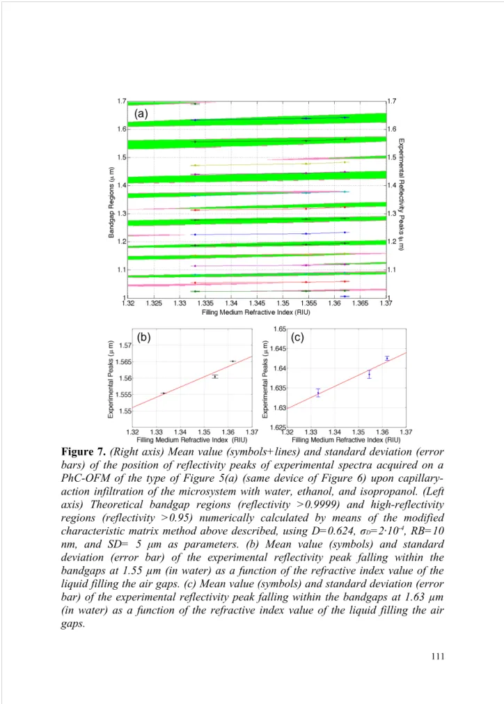
Figure 7. (Right axis) Mean value (symbols+lines) and standard deviation (error
bars) of the position of reflectivity peaks of experimental spectra acquired on a PhC-OFM of the type of Figure 5(a) (same device of Figure 6) upon capillary-action infiltration of the microsystem with water, ethanol, and isopropanol. (Left axis) Theoretical bandgap regions (reflectivity >0.9999) and high-reflectivity regions (reflectivity >0.95) numerically calculated by means of the modified
characteristic matrix method above described, using D=0.624, σD=2·10-4, RB=10
nm, and SD= 5 μm as parameters. (b) Mean value (symbols) and standard deviation (error bar) of the experimental reflectivity peak falling within the bandgaps at 1.55 µm (in water) as a function of the refractive index value of the liquid filling the air gaps. (c) Mean value (symbols) and standard deviation (error bar) of the experimental reflectivity peak falling within the bandgaps at 1.63 µm (in water) as a function of the refractive index value of the liquid filling the air gaps.
reflectivity spectra of Figure 6, which is in good agreement with SEM observation of micromachined surfaces and confirm the good optical quality of PhC fabricated by ECM technology.
Figure 7a (right axis) shows mean value (symbols+lines) and standard deviation (error bars) of the position of reflectivity peaks of experimental spectra acquired on a PhC-OFM of the type of Figure 5a (the same device of Figure 6) upon capillary infiltration of the microsystem with water, ethanol, and isopropanol. Despite the fact that no cover is bonded on top of the microsystem during capillary-action experiments, recorded spectra highlight that good repeatability is achieved both in air as well as with the liquid infiltrating the PhC structure (see Figure S2 supporting material), as it can be argued by standard deviation values reported in Figure 6. A good linear relationship is observed for any of the reflectivity peaks as a function of the refractive index value of the liquids infiltrating the air gaps , as it can be observed in Figure 7b and 7c for the peak at 1.55 μm and 1.63 μm, respectively. A maximum standard deviation value of about 1 nm is obtained over the whole set of peaks. Figure 7a (left axis) also shows theoretical bandgap regions (green areas) of the same 1DPhC in the wavelength interval under observation, from 1 μm up to 1.7 μm, as a function of the refractive index value of the medium filling the PhC air gaps, from 1.32 RIU up to 1.37 RIU. Bandgap regions are defined as wavelength intervals featuring a reflectivity value higher than 0.999 and were numerically calculated by means of the modified characteristic matrix method above described, using D=0.624, σD =2·10-4, RB=10 nm, and SD= 5 μm as
parameters. High reflectivity regions (pink areas), which are defined as wavelength intervals with reflectivity higher than 0.95, are also reported in Figure 7 and include, where existing, bandgap regions. Both position and width of the 1D-PhC bandgap regions significantly change with the refractive index value of the medium filling the air gaps, thus theoretically supporting the possibility of successfully using the proposed PhC structures as integrated devices for optofluidic applications, in general, as well as for label-free sensors, in particular. Experimental data on position and shift of reflectivity peaks as a function of the refractive index of the liquid infiltrated in the PhC structure (Figure 7a) well agree with theoretical predictions on the bandgap regions, apart from a few experimental reflectivity peaks that do not fall within the theoretical bandgap regions (green areas). The existence of such reflectivity peaks can be interpreted in terms of regions with high reflectivity, though lower than 0.999. Both position and shift of such experimental reflectivity peaks are in good agreement with numerically calculated high reflectivity regions (pink areas), as shown in Figure 7a.
In view of the application of the proposed PhC-OFMs as refractive index sensors an estimation of both sensitivity (S) and limit of detection (LoD) is performed by analyzing the experimental reflectivity peaks falling within the bandgaps at 1.55 µm and 1.63 µm (in water), which are the most significant both from research and commercial point of view. By best fitting experimental data with a linear
relationship, a sensitivity (defined as wavelength shift as a function of refractive index variation) S=dλ/dn=310 nm/RIU and 280 nm/RIU is obtained, respectively, which is comparable to refractive index sensors reported in the literature and exploiting photonic crystals. The use of a linear function for the fitting of experimental data is well supported by theoretical predictions, at least in the refractive index range investigated in this work [20]. An estimation of the actual limit of detection of the proposed PhC-OFM cannot be easily performed due to both the limited spectral resolution (0.8 nm) and the high value of the OSA resolution bandwidth (10 nm) required for ensuring sufficiently high signal-to-noise ratio and dynamics in the measurements. It is well known that the LoD value can be calculated as LoD=R/S, being R the system resolution that is typically established as 3·STD, with STD standard deviation of the noise in the system. The STD value can be expressed as is the variance of the quantization error due to spectral resolution limitation. For a fixed spectral resolution (SR) value, the resulting error can be modeled as quantization error, so that the error in determining the position of a reflectivity peak is uniformly distributed between -0.5·SR and +0.5·SR, and has a resulting standard deviation of 0.29·SR, that is STDspect-res=0.232 nm in this work. In addition, we expect that a significant contribution to the total STD of the system also comes from thermal-induced variation of system, as optofluidic measurements are performed at room temperature on PhC-OFMs that are not temperature-stabilized, as well as from amplitude noise sources. A worst-case estimation yields LoDworst=3·STD/S=4.8·10-3 RIU and 10.7·10-3 RIU for the reflectivity peak within the bandgap at 1.55 µm and at 1.63 µm (in water), respectively, which are calculated using the standard deviation maximum value of STD=0.5 nm and 1 nm obtained from experimental spectral measurements. It is expected that by reducing both the spectral resolution and the resolution bandwidth, for example reducing the wavelength step, using an amplified spontaneous emission source, and limiting the spectral measurement to a narrow wavelength interval around the bandgap of interest, and performing temperature stabilization of the OFM it is possible to significantly improve the LoD of the system.
3.2 Pressure-driven operation
Pressure-driven operation is investigated by injecting water, ethanol, as well as aqueous solutions featuring refractive index values between those of water and ethanol, in the PhC-OFM through the use of a syringe pump at flow rate of the order of 10 µl/min.
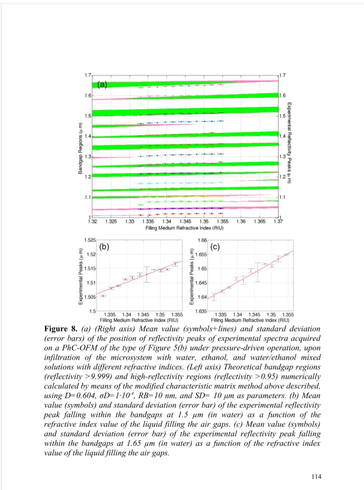
Figure 8a (right axis) shows mean value (symbols+lines) and standard deviation (error bars) of the position of reflectivity peaks of experimental spectra acquired on a PhC-OFM of the type of Figure 2 under pressure-driven operation, upon infiltration of the microsystem with water, ethanol, and water/ethanol mixed
Figure 8. (a) (Right axis) Mean value (symbols+lines) and standard deviation
(error bars) of the position of reflectivity peaks of experimental spectra acquired on a PhC-OFM of the type of Figure 5(b) under pressure-driven operation, upon infiltration of the microsystem with water, ethanol, and water/ethanol mixed solutions with different refractive indices. (Left axis) Theoretical bandgap regions (reflectivity >9.999) and high-reflectivity regions (reflectivity >0.95) numerically calculated by means of the modified characteristic matrix method above described,
using D=0.604, σD=1·10-4, RB=10 nm, and SD= 10 μm as parameters. (b) Mean
value (symbols) and standard deviation (error bar) of the experimental reflectivity peak falling within the bandgaps at 1.5 µm (in water) as a function of the refractive index value of the liquid filling the air gaps. (c) Mean value (symbols) and standard deviation (error bar) of the experimental reflectivity peak falling within the bandgaps at 1.65 µm (in water) as a function of the refractive index value of the liquid filling the air gaps.
solutions with different refractive indices. A good linear relationship is observed for any of the reflectivity peaks as a function of the refractive index value of the liquids infiltrating the air gaps. A maximum standard deviation value of about 3 nm is obtained over the whole set of peaks, thus indicating that good repeatability is obtained after cycling the different liquids several times through the microsystem (see Figure S3 in supporting information). Figure 8a (left axis) also shows theoretical bandgap regions (green areas) and high reflectivity regions (pink areas) of the same 1DPhC in the wavelength interval under observation, from 1 μm up to 1.7 μm, as a function of the refractive index value of the medium filling the PhC air gaps, from 1.32 RIU up to 1.37 RIU. Bandgap regions and high-reflectivity regions were numerically calculated by means of the modified characteristic matrix method above described, using D=0.604, σD =1·10-4, which are obtained by best
fitting experimental reflectivity spectra in the whole wavelength range under observation, using RB=10 nm and SD = 10 μm. Figure 8b and 8c show experimental reflectivity peaks falling within the bandgaps at 1.5 µm and 1.65 µm (in water), respectively, as a function of the refractive index value of the liquid filling the air gaps. By best fitting experimental data of Figure 8b and 8c with a linear relationship, a sensitivity S=dλ/dn=460 nm/RIU and 670 nm is obtained, respectively. A worst-case estimation of the limit of detection yields LoDworst=3·STD/S=17.6·10-3 RIU and 13.4 ·10-3 RIU for the reflectivity peak within the bandgap at 1.5 µm and 1.65 µm (in water), respectively, which are calculated using the standard deviation maximum values STD=2.7 nm and 3 nm obtained from experimental spectral measurements. It must be pointed out that LoD values are in this particular case limited by the standard deviation of the spectral measurements performed with the solution containing 60% of ethanol in water, which is clearly an outlier in the whole set of measurements, probably due to air bubbles traveling in the 1DPhC during one of the measurement cycles with this specific solution. If we recognize the error bar of the measurement with the mixture containing 60% of ethanol in water as an outlier, we can exclude it from the LoD calculation, thus reducing the LoD value to 4.5·10-3 RIU and 5.8·10-3 RIU. 4. Conclusion
In this work, the realization of all-silicon optofluidic microsystems (OFMs) of the second generation, in which high aspect-ratio (HAR) photonic crystal (PhC) devices (i.e. micromirrors, optical cavities) are integrated on the same silicon die together with microfluidic reservoir/channels for the infiltration of liquids in the PhC air gaps, and with fiber grooves for alignment/positioning of readout optical fibers in front of the PhC, is for the first time demonstrated to be feasible in any lab at low cost and with high flexibility by using the electrochemical micormachining (ECM) technology.
Fabrication of PhC-OFMs by ECM technology is performed through the exploitation of a dynamic control of the etching anisotropy as the electrochemical
etching progresses, which allows the silicon dissolution to be effectively switched in real-time from the anisotropic regime to the isotropic regime and enables advanced silicon microstructuring to be carried out through the use of both functional and sacrificial structures, with submicrometric accuracy at aspect-ratio values not manageable by up-to-date wet and dry technologies. In particular, surface quality of ECM-fabricated HAR-PhC structures, with peak-to-valley estimated to as low as few nanometers and deviation from vertically of about 0.02° up to depth of 100 µm, is superior to that of state-of-the-art DRIE etching technologies at the HR values reached in this work.
Optofluidic characterization of PhC-OFMs is successfully demonstrated by both capillary action and pressure-driven operation, through measurements of the reflectivity spectra of HAR-PhCs upon injection of liquids featuring different refractive index values in the HAR-PhC air gaps, by using readout optical fibers positioned in the on-chip fiber grooves. On the one hand, pressure-driven operation allows PhC-OFMs to be tested upon connection with a standard syringe pump (or peristaltic pump) and an external reservoir, which is mandatory for future biosensing applications of PhC-OFMs. In fact, biosensing applications require, for example, an effective immobilization on the PhC inner surface of suitable biological recognition elements capable of selectively binding specific target analytes to be performed via fluid flow through the PhC of proper solutions. On the other hand, capillary action operation opens new exciting possibilities of concerning a drop-and-measure approach for such PhC-OFMs, which allows detection of specific analytes to be performed on already-functionalized OFMs with out the need of connection to fluidic peripheral equipments, thus reducing both volume and waste of biological samples as well as power dissipation and size, while increasing portability and point-of-care operation. High sensitivity and good limit of detection for the PhC-OFMs of this work are obtained both for capillary-action and pressure-driven operation, with a best sensitivity value of 670 nm/RIU, which is comparable to state-of-the-art integrated refractive index sensors, and a best limit of detection of the order of 10-3 RIU, which is significantly limited by constraints of the experimental setup and is expected can be strongly improved by providing the measurement setup with temperature control system as well as by recording the reflectivity spectra with smaller spectral resolution and reduced resolution bandwith.
Acknowledgments This research was partially supported by PRINMIUR and CARIPLO Foundation.
5. Materials and Methods
Design rules: The layout design of PhC-OFMs fabricated by ECM technology was
carried out according to the following main rules: 1) porosity of functional structures, that is silicon areas patterned with anchor structures and photonic
crystal structures, was set by design to a value of 20% for the former and 50% for the latter; 2) after functional structures were properly designed, the remaining silicon area was partitioned with sacrificial structures with porosity value of 50% by design; 3) two layout elements were by design separated by a distance with minimum dimension of 2 µm and maximum dimension of 4 µm; 4) each layout element had by design a width ranging between a minimum dimension of 2 µm and a maximum dimension of 6 µm; 5) anchor structures were designed to enclose parts sufficiently larger than sacrificial structures, in order to effectively withstand the isotropic phase of the electrochemical etching step; 6) sacrificial structures consisted of basic elements (i. e., a straight line with proper length and width), designed to become free-standing during the isotropic phase of the electrochemical etching, which were arranged as one-dimensional array of parallel lines, with number of elements and array orientation chosen to comply with issues 2) and 3). For the sake of clarity, the design values of structural and sacrificial structures used for the fabrication of the microsystem in Figure 2 are here below provided. Anchor structures consisted of a two-dimensional repetition of a 5x5 square lattice of holes side of 4 µm and pitch of 8 µm enclosed by a silicon frame with width of 6 µm; photonic crystals consisted of one-dimensional array of 850-µm-long parallel lines with a width of 4 µm and a pitch of 8 µm; basic elements of sacrificial structures consisted of straight lines with width of 2 µm and pitch of 4 µm.
Silicon wafers: All the experiments were carried out on (100) n-type CZ-grown
silicon substrates, provided by STMicroelectronics, with resistivity 2.5-8.5 Ω·cm. A 200-nm-thick silicon dioxide was grown by dry thermal oxidation in pure O2 atmosphere at 1050 °C for 4h, in a ThermoLyne 21100 tube furnace.
Pattern definition: An Microposit S-1818 photoresist (from Shipley) film was
deposited on the silicon wafer by spin-coating at 4000 rpm for 60 s and subsequent soft-baking on hot-plate at 115 °C for 90 s. UV contact lithography system (MJB3 Karl-Suss mask aligner) was used for layout pattern definition. Photoresist development and post-backing were carried out by using 1:5 (by volume) Microposit developer 351:H2O solution and hot-plate at 115 °C for 90 s, respectively. Once the lithographic step was ended, the layout pattern was transferred to the silicon dioxide layer by wet etching in a 6% wt. buffered HF (BHF) solution for 120 s.
KOH etching: The pattern was transferred to the silicon substrate by wet etching in
a 25 wt% KOH solution, saturated with isopropanol to improve the etching uniformity, at 50 °C. The etching time was chosen long enough to obtain formation of full-V grooves for all patterned geometries. The oxide layer, which was used as masking layer during the alkaline etching, was removed after that by wet etch in a 1:1 (by volume) HF (48%):ethanol (99.9%) solution.
Electrochemical etching (BIEE): The experimental setup used for the
electrochemical etching was constituted of a PTFE (Polytetrafluoroetylene) electrochemical cell having a volume of 400 cm3. The front side of the silicon sample was in contact with the solution. The area of the sample exposed to the electrolyte was about 0.66 cm2 and had a circular shape. The electrolyte composition was 5 vol% HF:95 vol% H2O, with 1000 ppm of Sodium Lauryl Sulfate (SLS) as wetting agent. The surfactant was added to reduce the formation of hydrogen bubbles at the sample surface, thus enhancing the etching uniformity. For the same reason, the solution was stirred during the anodization process. Back side illumination of the sample was performed with a 250 W halogen lamp, positioned about 6 cm apart from the sample, through a circular window (0.66 cm2) in the metal electrode used to provide the electrical contact to the sample. A feedback loop, performed by using a PID controller (Eurotherm 2604), allowed the lamp power, and thus the illumination intensity, to be changed in order to proper set the etching current density value as the etching progressed. An IR filter with a cutoff wavelength of 750 nm was placed between the lamp and the silicon sample in order to avoid carrier generation close to the silicon surface in contact with the electrolyte. A second feedback loop, also obtained with the same PID controller, allowed the working temperature to be maintained at 22 °C for the entire etching time. The cathode consisted of a platinum disc in front of the silicon anode at a distance of 1 cm, whereas a platinum wire close to the silicon electrode, at a distance of about 2 mm, is used as a pseudo-reference electrode. A Source Measure Unit (Keithley 2410 Source Meter) was used to apply the anodization voltage, between the silicon sample and the reference electrode, and to monitor the etching current.
J-V curves required to obtain the ECM working region of the electrochemical system under investigation were recorded under back-side high-intensity illumination of the silicon electrode, by driving the halogen lamp at its maximum power value (250 W). The electropolishing etching current density and voltage values were Jpeak = 64.79 mA/cm2 and Vetch= 0.8V.
As to the anisotropic phase, the etching voltage Vetch was set to a constant value of 3 V for the entire etching process, while the etching current density is set to an initial value Jethc0 = 35.17 mA/cm2 and linearly reduced over time with a rate of 2.5 µA/cm2/s according to a first-order approximation of the diffusion kinetics of HF molecules from top to bottom of the etched structures, in order to get a constant porosity and, in turn, a perfect anisotropic etching throughout the whole etching depth [41]. The Jethc0 value was tailored on the basis if the Jpeak value in order to obtain a constant porosity mean value of the whole microsystem of 55%, which was experimentally found to give rise to photonic crystal and sacrificial structures with porosity of 62% and anchor structures with porosity of 43%. In fact, experimental observations performed by SEM analysis on a large set of
ECM-fabricated complex microsystems containing silicon areas patterned with structures with fairly different geometry, such as sacrificial and anchor structures, highlight that though the mean value of the porosity of the whole microsystem is actually set by the Jethc value, the specific porosity value of each patterned area significantly depends on the pattern features (e.g. layout porosity, pattern geometry, etc.) in a non-trivial way. For instance, Pavg=Jetch/Jpeak=Vetched/Vtot=(P1A1 + P2A2)/Atot=0.53 which is close to the expected average value of the microsystem porosity, being P1=0.62 and A1=0.24 cm2 experimental porosity and area of photonic crystal and sacrificial structures, respectively; P2=0.4218 and A2=0.42 cm2 experimental porosity and area of anchor structures; Atot=0.66 cm2 the whole silicon area subjected to electrochemical etching. The etching time of the anisotropic phase tetch=3900 s was chosen to fully etch 95-µm-deep trenches.
As to the isotropic phase, after the desired depth was obtained, the value of Jetch was abruptly increased from 25.32 mA/cm2 , which corresponds to the etching current density value at the end of the anisotropic phase, to 40.32 mA and kept constant for the next 150 seconds in order to isotropically etch the silicon for a further depth of 5 µm.
Glass slab: A milling machine (CAM-100 VHF) digitally automated via computer
numerical control (CNC) and equipped with a diamond tip was used to drill two through-holes (1.2 mm diameter), 4 mm far apart, in a borosilicate glass slab (800 µm thick) to be used as a chip cover.
Anodic bonding: The glass cover was anodically bonded to the micromachined
silicon substrate using a voltage of 600V at the temperature of 400 °C. In order to remove organic contaminants off the substrates, the micromachined silicon substrate and glass cover were immersed before bonding in Piranha solution, consisting of 1:1 (by volume) H2SO4(96%):H2O2(30%), heated at the temperature of 100 °C. The silicon substrate was then rinsed in 1:1 (by volume) HF (48%):ethanol (99.9%) solution for 120 seconds to remove from the silicon surface thin oxide layer formed during previous cleaning step. After bonding, the microsystem was equipped with two stainless steal fitting ports having internal/external diameter of 1.0/1.2 mm and allowing easy-to-use fluidic connections of the chip to an external setup.
Optical measurements: Measurements of spectral reflectivity on PhC-OFMs were
performed with the optical setup reported in Figure S4 (Supporting material). Fiber groove and photonic crystal sensing region were monitored on a computer by placing the PhC-OFM under a microscope connected to a digital CMOS camera. Radiation in the range 1.0 µm -1.7 µm generated by a white lamp was launched toward the PhC by means of a standard telecom SMR-28 (9/125/250 µm core/cladding/coating diameter) fiber-optic 50% coupler, which also carried the
reflected light back to the optical spectrum analyzer (OSA). For the measurements on PhC-OFMs without glass cover, exploiting capillary action, a tapered lensed fiber with standard 125-µm diameter (from ozOptics ) was connected to the output port of the coupler and the lensed tip was laid down on the bottom of the groove. A beam spot diameter of 5 µm on the front facet of the PhC was typically obtained. Reflectivity measurements on PhC-OFMs equipped with glass cover, exploiting pressure-driven operation, were performed by using a home-made reduced-diameter (approximately 65-85 µm) fiber tip with a 1° angled termination, which was obtained from a standard 125-µm diameter fiber (SMR-28), positioned in the fiber groove. A beam spot diameter of 10-12 µm on the front facet of the PhC was typically obtained. Fiber positioning in the groove was performed in both cases by means of a manual nanopositioning xyz stage. The fiber-tip/PhC optimal working distance was obtained by maximizing the reflected power in bandgap wavelength regions, and was of about 26 µm for the lensed fiber and 16 µm for the home-made tip. The 1°-angled termination of the home-made reduced tip did not completely eliminate the Fabry-Perot cavity effect between fiber tip and PhC, which was neglectable with the lensed termination. On the other hand, the residual ripple on reflectivity spectra with the 1°-termination tip did not affect reflectivity peak recognition. A few preliminary experiments were performed on reference PhC samples for directly comparing the results obtained with lensed-tip and home-made termination fibers. Apart from the residual ripple, the spectral lineshapes were similar, though deeper reflectivity notches could be observed with the lensed fiber due to the smaller spot diameter [35]. Normalization of the reflected power spectra with respect to an ideal reflector was carried out by numerical elaboration using the glass-air interface at the output connector as reference [35].
Optical fiber thinning: Home-made optical fibers with reduced-diameter were
prepared by means of an optical fiber thinning procedure consisting of a HF-based etching step, which was used to reduce the diameter of standard telecom SMR-28 fiber from 125 µm to 65-85 µm, and a final mechanical lapping step, which was used for shaping the optical fiber termination. A 5-cm-long SMR-28 fiber was mechanically denuded of the acrylic coating, cleaned in ethanol, and then rinsed in a HF-based solution at room temperature for 25 minutes and 30 minutes in order to reduce the fiber diameter in the range of 80-85 µm and 65-70 µm, respectively. After the thinning procedure was performed, etched fibers were washed in DI water. Optical fibers with 1°-angled termination were produced by means of a further mechanical lapping procedure. Thinned fibers were inserted into a glass capillary and fixed with a drop of glue (Norland Optical 61) at the tip. The capillary-fiber assembly was mounted on a lapping machine at an angle of 1° degree with a respect to optical fiber axis and then sequentially polished by means of abrasive papers with micrometer grit values of 12 µm, 8 µm, 3 µm, 1 µm, and
0.3 µm. Finally, as shaped fibers were unmounted from the capillary and residual glue were removed in dichloromethane solutions.
Reference
__________________________________________________________________
[1] X. Fan and I. M. White, Nature Photonics 2011, 5, 591; [2] Y. Zhao , X. Zhao, Z. Gu, Adv. Funct. Mat. 2010, 20, 2970;
[3] S.-K. Hoi , X. Chen , V. S. Kumar , S. Homhuan , C.-H. Sow., A. A. Bettiol, Adv.
Funct. Mat. 2011, 21, 2847;
[4] K. Tsioris, G. E. Tilburey, A. R. Murphy, P. Domachuk, D. L. Kaplan, F. G. Omenetto,
Adv. Funct. Mat. 2010, 20, 1083;
[5] J. D. Joannopoulos, S. G. Johnson, J. N. Winn, R. D. Meade, in Molding the Flow of
Light, Pronceton, Princeton University Press, 2nd ed., 2008;
[6] K. Sakoda, in Optical Properties of Photonic Crystals, New York, Springer, 2nd ed.,
2005;
[7] E. Yablonovic, Phys. Rev. Lett. 1987, 58(20), 2059; [8] S. John, Phys. Rev. Lett. 1987, 58(23), 2486;
[9] G. von Freymann, A. Ledermann, M. Thiel, I. Staude, S. Essig, K. Busch, M. Wegener,
Adv. Funct. Mat. 2010, 20, 1038;
[10] M. van den Broek, L. A. Woldering, R. W. Tjerkstra, F. B. Segerink, I. D. Setija, W. L. Vos, Adv. Funct. Mat. 2012, 22, 25;
[11] D. Erickson, D. Sinton, D. Psaltis, Nature Photonics 2011, 5, 583;
[12] X. Hu, Z. Li, J. Zhang, H. Yang, Q. Gong, X. Zhang, Adv. Funct. Mat. 2011, 21, 1803; [13] C. I. Aguirre, E. Reguera, A. Stein, Adv. Funct. Mat. 2010, 20, 2565;
[14] Z. Wang, J. Zhang, J. Xie, C. Li, Y. Li, S. Liang, Z. Tian, T. Wang, H. Zhang, H. Li, W. Xu, B. Yang, Adv. Funct. Mater. 2010, 20, 3784;
[15] C. J. Choi, B. T. Cunningham, Lab Chip 2007, 7, 550;
[16] S.-K. Lee, S.-G. Park, J. H. Moon, S.-M. Yang, Lab Chip 2008, 8, 388; [17] S. Mandal, J.M. Goddard, D. Erickson, Lab Chip 2009, 9, 2924;
[18] P. S. Nunes,N. A. Mortensen, J. P. Kutter, K. B. Mogensen, Opt. Lett. 2008, 33(14), 1923.