Università degli Studi di Napoli Federico II
DOTTORATO DI RICERCA IN
FISICA
Ciclo XXXICoordinatore: Prof. Salvatore Capozziello
Investigation of graphene as electrode
in n-type OFETs and its use in
nanometric devices
Settore Scientifico Disciplinare FIS/01
Dottorando Tutore
Federico Chianese Prof. Antonio Cassinese
"Ignoranti quem portum petat nullus suus ventus est." -Seneca, Lettere a Lucilio-
i
C
ONTENTS
Introduction ... 1
1
Organic-Field-Effect-Transistors ... 4
1.1
Organic Semiconductors ... 5
1.1.1
n-type and p-type organic semiconductors ... 7
1.1.2
PDIF-CN2 and PDI8-CN2 as n-type organic semiconductors ... 9
1.2
Working principles ... 11
1.2.1
Current-Voltage characteristics ... 12
1.3
Contact resistances and electrode/organic interfaces in OFETs. ... 16
1.3.1
Contact Engineering in OFETs ... 19
1.3.2
Measuring techniques for contact resistances ... 21
1.4
Transistor operation in dynamic regime ... 23
1.5
Short channel effects in nanometric architectures ... 26
1.6
Graphene ... 29
1.6.1
Electronic Properties ... 30
1.6.2
Charge Transport ... 32
1.6.3
Quantum capacitance ... 34
1.6.4
Doping effects ... 36
1.6.5
Production methods of graphene ... 37
1.7
Graphene as novel electrode material for organic electronics ... 39
2
Device Fabrication ... 43
2.1
Electron Beam Lithography ... 43
2.1.1
The EBL experimental set-up ... 44
2.1.2
Enhanced sensitivity of PMMA 950K as positive e-resist using amyl
acetate-based developers. ... 46
2.2
Reactive Ion Etching ... 48
ii
2.4
Bottom-contacts/Distributed-bottom-gate nano-OFET layout ... 50
2.4.1
Gold-based nano devices ... 54
2.5
Bottom-contacts/Local-gate nano-OFET layout ... 55
2.6
Micrometric bottom-contacts/distributed-bottom-gate interdigitated
architectures ... 58
2.7
Organic thin film growth ... 59
2.7.1
Perylene diimides thin films by Organic Molecular Beam Deposition
………. 62
3
Graphene Electrodes in nanometric Architectures ... 64
3.1
PDIF-CN2 based bottom-contacts/distributed-bottom-gate OFETs .... 65
3.1.1
Morphological characterization ... 65
3.1.2
DC electrical Characterization ... 66
3.1.3
Gold electrodes Vs Graphene electrodes in nanometricarchitectures
... 68
3.1.4
Doping conditions of CVD-Graphene Electrodes ... 72
3.2
PDI8-CN2 based nanometric OFETs with Local gate and ultra-thin
Hafnium Dioxide as dielectric ... 75
3.2.1
CVD-Graphene on ultra-thin HfO
2... 75
3.2.2
Current-Voltage characteristics ... 79
3.2.3
AC characterization ... 82
3.2.4
Capacitance contribution of graphene electrodes ... 83
3.2.5
Calculated Cut-off frequencies for short channel OFETs ... 87
3.3
Final Discussion ... 88
4
The Graphene/Organic interface ... 91
4.1
Scanning Kelvin Probe Force Microscopy ... 92
4.2
Contact effects in gold-based micrometric devices ... 95
4.3
micrometric devices with CVD-Graphene Electrodes ... 101
4.3.1
Transport properties of CVD-graphene electrodes ... 102
iii
4.3.3
Surface Voltages Profiles and Contact Resistances via SKPFM ... 106
4.4
Surface Spectroscopy via UPS/XPS ... 110
4.4.1
X-ray photoelectron spectroscopy ... 111
4.4.2
XPS analysis of PDI8-CN2 and PDIF-CN2 reference films ... 112
4.4.3
UV photoelectron spectroscopy... 116
4.4.4
UPS analysis of the organic/graphene interfaces ... 117
4.5
Final Discussion ... 122
5
Conclusions ... 124
1
Introduction
In the last years, scientific attention has been actively focused on the possible technological breakthrough of organic electronics and on the effective application of its paradigms, consisting in the production of flexible, low cost and easy-to-process devices for mass consumer electronics. Rapid advancements in the field prompted the development of a wide number of organic devices such as light-emitting diodes (OLEDs), solar cells, memories, light emitting field-effect transistors (OLETs) and organic-field-effect-transistors (OFETs). Specifically, OFETs have significantly improved in the past decade with nowadays benchmark devices competing with amorphous silicon thin-films-transistors (TFTs) in terms of electrical performances. However, further improvements are still necessary to maximizes output currents and switching frequency, with a significantly reduction of the required supply voltages at the same time. All these assessments are typically addressed in terms of the enhancement of charge mobility. A different approach for improving OFET performances is to intervene on the device architecture rather than on transport properties of the organic semiconductors, with the downscaling of channel lengths L, which are typically in the micrometer scale, into the sub-micrometer regime. On the other hand, the reduction of lateral dimension is typically accompanied by the rising of short-channel effects heavily interfering with a proper functioning of the organic devices.
Moreover, in the last years scientific community witnessed the relentless rise of the graphene: a carbon-based one-atom-thick material that combines high electronic and thermal conductivities, and extreme mechanical strength. Huge effort has been spent in the solid-state research to develop new technological applications of such a material. Among them, graphene has been recently considered as an interesting electrode material in organic field-effect devices, taking advantages from its work function tunability, permeability to the transversal electric field, and overall chemical stability.
The aim of this thesis concerns the investigation of graphene as electrodes in OFETs based on perylene tetracarboxylic diimides derivatives as n-type organic semiconductors. In particular, the role of graphene has been explored in relation with the downscaling of the lateral dimensions of the devices towards nanometric architectures. The electronic and morphological peculiarities of graphene electrodes have been demonstrated to play a key role in the mitigation of short-channel effects, typically encountered in gold-based devices. High quality transistor operation is observed for channel lengths down to 𝐿 ≈ 150 − 200𝑛𝑚 while long-channel (micrometric) devices shows substantially state-of-the-art performances if directly compared to gold-based layouts with similar architectures.
The thesis is divided in four chapters. In the 1st chapter, a brief introduction to the semi conductive properties of π-conjugated molecules will be reported. A digression on the organic compounds will stress the differences between n-type and p-type conduction giving particular attention to the properties of two electron-transporting organic molecules: PDIF-CN2 and PDI8-CN2. The operating mode of the organic thin film
2
transistor will be discussed, borrowing the theoretical considerations from inorganic MOSFETs and outlining the main differences. The discussion will continue describing the contact effects occurring at the organic-semiconductors/electrode interfaces as well as the widely employed technique for the measurements of contact resistances. The downscaling of lateral dimensions of OFETs will be addressed by discussing the main theoretical considerations on short-channel effects and their influence in nanometric architectures reported in literature. The role of the channel length L will be highlighted in the description of the dynamic regime of operation in OFETs. The second part of the chapter is devoted to the introduction to graphene and its properties, with particular attention to the experimental techniques typically employed for the estimation of its transport properties, the quantum capacitance contribution in state-of-the-art graphene-based devices and the procedures commonly employed for its production. In the last section, the use of graphene as novel electrode material in organic devices will be addressed.
The 2nd chapter is devoted to the description of the experimental set-ups employed for the fabrication of both nanometric and micrometric architectures based on graphene electrodes by means of Electron-Beam-Lithography (EBL). A brief digression will be presented on the observed enhanced sensitivity of standard PMMA950K through amyl-acetate developers. The detailed fabrication recipes of three main architectures will be given. The discussion will move to the deposition methods for the organic semiconductors via the Organic Molecular Beam Deposition (OMBD) technique, describing the employed experimental set-up and focusing the attention on the deposition of perylene diimides thin films.
The 3rd chapter focuses on the experimental results obtained from the characterization of the nanometric channel n-type PDIF-CN2 OFETs based on graphene electrodes. In the first paragraph, by a thorough comparison with short channel transistors made with reference gold electrodes, an overall suppression of short-channel effects will be demonstrated for the graphene-based counterpart. The lack of current saturation in the output characteristics, due to the presence of a relatively thick distributed gate electrode of this architecture (SiO2 300nm), is overcome in the second paragraph of the chapter, where the results will be reported for an alternative optimized layout with local gate electrodes and ultra-thin hafnium dioxide as high-k dielectric. The mitigation of short channel effects will be proved to still hold in the case of PDI8-CN2 thin films. Moreover, the AC characterization of devices will highlight the contribution of the quantum capacitance of graphene electrodes on the overall switching capabilities of the nano OFETs in dynamic regime.
The 4th chapter will give further insights on the organic/graphene interfaces, particularly in the case of long channel (micrometric) OFETs with graphene electrodes. Particular attention will be given to the contact resistances and their measurement by means of Scanning Kelvin Probe Force Microscopy (SKPFM). A brief description of the technique and of the experimental set-up will be given. The analysis will focus on the comparison between the contact effects in graphene-based layouts and their state-of-the-art counterpart with gold electrodes. The last section concerns on surface spectroscopy of
3
the organic/graphene interfaces, investigated by means of UV Photoelectron Spectroscopy (UPS) and X-ray Photoelectron Spectroscopy (XPS).
4
1 O
RGANIC
-F
IELD
-E
FFECT
-T
RANSISTORS
The discovery of the first highly conducting polymer (chemically doped polyacetylene) in 1977 [1] resulted in a huge research effort on organic materials that led to the firstly reported p-type Organic-Field-Effect-Transistor (OFET) in 1986 [2].
Nowadays, the unique processing characteristics and demonstrated performance of OFETs suggest that they can be competitive candidates for existing or novel thin film transistor applications requiring large area coverage, structural flexibility, low temperature processing, and especially low production cost. Despite the potential technological applications, several bottlenecks still restrict their miniaturization towards the nanometric scale.
This first chapter will introduce to the scientific topic with a brief digression on the definition of organic semiconductor, with particular attention to the difference with the inorganic counterparts in terms of electronic structure of organic solids and transport mechanisms. Once introduced to the working principles of OFETs, contact effects affecting organic devices and their implication in terms of electrodes engineering will be discussed. The second part of the chapter is intended to briefly introduce to the utterly vast topic concerning graphene and its application. The digression will focus mostly on the experimental aspects that are preparatory for the discussion of experimental results reported in the following chapters.
5
1.1 O
RGANIC
S
EMICONDUCTORS
Organic semiconductors (OSCs) are usually hydrocarbon molecules or polymers with a core of sp2 hybridized carbon atoms. In sp2 configuration, the 2s, 2px and 2py atomic orbitals forms three pairs of in-plane bonding (σ) and antibonding (σ∗) molecular orbitals. The remaining pz atomic orbital forms a pair of π and 𝜋∗ hybrid orbitals, perpendicular to
plane individuated by the 𝜎 bonds. The 𝜋-𝜋∗ couple is delocalized over the entire organic molecule that is thus referred as 𝜋 -conjugated. In the ground state, all the molecular orbitals are filled by an antiparallel-spin electron pair up to the highest occupied molecular orbital (HOMO). The antibonding orbitals, from the lowest unoccupied molecular orbital (LUMO) onwards, are empty (Figure 1.1 a). In organic semiconductors, the energy difference between HOMO and LUMO acquires the role of the bandgap of the inorganic counterpart. For increasing molecular mass, the confinement effects on electrons are weakened and the HOMO-LUMO gap is reduced.
In conventional inorganic semiconductors, strong covalent bonds between the atoms lead to significant overlaps of the electronic orbitals, resulting in broad energy bands. In organic solid, on the contrary, the magnitude of the interactions between molecules is limited to weak van der Waals forces. Wave functions of the HOMO and the LUMO are mainly localized in each molecule resulting in narrow gaussian-shaped energy bands, typically only few hundreds of meV wide [3] (Figure 1.1 b).
Figure 1.1 (a) Electronic structure of a single molecule and (b) band structure for an organic solid. Adapted
from [4].
The more complicated geometry of organic molecules compared with the simple, spherical atoms and ions that constitute the inorganic semiconductors render most of the organic semiconductors rather disordered. All these factors limit the ability of intermolecular charge transfer in the organic solid and consequently influence the charge carrier mobility 𝜇. Since the huge variety of organic compounds and in great number of extrinsic parameters influencing 𝜇, there is no model that comprehensively describes the charge transport in all organic semiconductors.
In conventional inorganic semiconductor charge carriers moves freely in a wide band as propagating Bloch waves. In organic semiconductors, this charge transport mechanism
6
has been observed only at low temperatures for which 𝜇 ∝ 𝑇−𝑛, with 𝑛 > 0. A band model description has been proved to be suitable in describing charge transport at very low temperatures for naphthalene single crystals [5,6]. In general, organic semiconductors are in the form of polycrystalline films or even amorphous solids. Charge transport in organic semiconductor devices is therefore usually determined by localized states in the forbidden energy gap. These states can be created by energetic and positional disorder, which includes impurities, defects, grain boundaries and interface states. For example, for organic solids in which disorder is not dominating, it is possible to apply the so-called Multiple-Trap-and-Release model (MTR) [7]. MTR has been used to account for gate voltage dependent mobility in hydrogenated amorphous silicon [8] and then extended successfully to polycrystalline oligothiopene thin-films [9]. The model assumes the presence of localized states in the HOMO-LUMO bandgap. The shallow trap can exchange carriers with the extended band states through the competing processes of trapping and thermal excitation (Figure 1.2a), thus reducing the effective carrier mobility with an Arrhenius-like behavior of the form:
𝜇MTR= 𝜇0𝛩𝑡exp (−𝐸𝐶− 𝐸𝑡
𝑘𝐵𝑇 ) (1.1)
where μ0 indicates the intrinsic trapping-free mobility of the organic semiconductor, Θ𝑡 is the ratio between the density of transport free states and the trapping states while 𝐸𝐶 and 𝐸𝑡 individuate the conduction and the trapping level, respectively.
Variable-Hopping-Range (VHR) models, on the other hand, can be applied when disorder can be considered as dominating [10]. Localized charge carriers may travel through the material by hopping from one localized state to the next by phonon-assisted tunneling (Figure 1.2b). The transition probability (𝑊𝑖𝑗) between an occupied state with energy 𝐸𝑖 and a free state 𝐸𝑗, separated by a hopping distance 𝑅𝑖𝑗, can be described by the Miller-Abrahams expression [11,12]:
𝑊𝑖𝑗 = 𝜈0𝑒𝑥𝑝(−γ|𝑅𝑖𝑗|) {exp (−
𝐸𝑗− 𝐸𝑖
𝑘𝐵𝑇 ) ∀𝐸𝑗 > 𝐸𝑖
1 𝑒𝑙𝑠𝑒 (1.2) where 𝜈0 is a characteristic vibration frequency of the material while γ is defined as an the inverse of the localization radius.
7
Figure 1.2 Schematic illustrations of disorder-based transport models in organic semiconductors. (a) In
Multiple-Trap-and-Release model (MTR), charge carriers trapped in localized states in the forbidden band are thermally released towards the conduction band. (b) In Variable-Range-Hopping (VRH) models, phonon assisted tunneling between localized states dominates the transport in the organic semiconductors. Furthermore, in organic semiconductors electron-phonon coupling no longer plays the role of a perturbation, as in the case of covalently bound inorganic semiconductors, but rather leads to the formation of polarons for which mobility results strongly temperature dependent [13]. At this regard, the dynamic interaction between the traveling charges and the molecular vibrations has been recently measured in rubrene single crystals via angle resolved UV photoelectron spectroscopy [14].
1.1.1 n-type and p-type organic semiconductors
For organic semiconductors, the common p−type or n−type classification does not apply since organic compounds can be considered as intrinsic. It rather expresses the ease with which one of the charge carriers can be injected through the metal electrodes. One of the most important aspects of charge injection is, indeed, the energy levels alignment at the interfaces.
Lowering energetic barriers facilitates efficient injection resulting in enhanced electrical performances. The energy levels matching at electrode/organic interface can be achieved through the proper selection of the metal in comparison with HOMO or LUMO levels of the organic semiconductors. In particular, referring to the Fermi energy (Ef) of the metal electrode, low Ef-LUMO barrier yields to an assisted electron injection; on the contrary, low Ef-HOMO barrier is characterized by hole injection (Figure 1.3).
(a)
8
Figure 1.3 Schematic showing the Fermi-Dirac occupation function with Fermi level 𝐸𝐹 for the metallic side
of the interface. The difference in energy between 𝐸𝐹 and the onsets of occupied and unoccupied density of
states (DOS) on the organic semiconductor side are the charge injection barriers Δℎ for holes and Δe for
electrons, respectively.
However, a simplistic energy-band diagram only provides a guide for selecting contact materials and the use of an electrode with a properly selected work function does not guarantee efficient hole or electron transport and improved device performances. As it will be further discussed in the next sections, charge injection and extraction at the OSC/electrode interface are not trivial phenomena and numerous parameters must be taken into account when estimating the energy barriers.
In the past few years, remarkable improvements have been made in enhancing the charge carrier mobility of p-type OSCs thanks to the development of new materials, and device architecture optimization. Charge carrier mobility values exceeding 40 cm2V-1s-1 have
been achieved for both p-type small molecules [15–17] and highly oriented nanocrystalline hole-transporting polymers [18], in OFETs configurations. On the other hand, the overall development of n-type organic semiconductors still lags behind their p-type counterparts in terms of ambient stability and mobility which is still confined in the order of few cm2V-1s-1 [19]. To move ahead with organic electronics, nevertheless,
research activity on n-type OSCs is of vital importance for the development of complementary logic for digital applications. One of the main challenges for n-type organic semiconductors is the injection of electrons from a suitable electrode to the LUMO level of the organic compound. In the p-type counterparts, HOMO levels in the range between 4.8eV and 4.3 eV are typically observed. These values are easily aligned with the work function of the most widely used metallic electrodes, as for example gold which has a work function ranging between 4.8eV and 5.1eV. For n-type OSCs, LUMO levels are in the range of 3-4eV. Observation of n-type behavior is thus severely limited due to the extremely high injection barrier in the case of Au/OSC interfaces. Increasing electron affinity (i.e. lowering the LUMO level) of the organic compound is thus a valuable route for enhancing electron-transporting properties. This is usually achieved by taking a known semiconducting core molecule and adding strong electron withdrawing groups
9
such as fluorine, cyano, or iimide moieties [20]. Another strategy for the reduction of the metal/OSC energy barrier would imply the use of high work function metals such as Aluminum, Calcium, Chromium. In this case, major drawbacks are clearly due to the high oxidizing nature of those materials, degrading the reliability of the contacts and the overall performances of the organic device.
Even if the chemical tailoring of the molecule and the choice of the electrode material ensure the electron transporting properties, the susceptibility of n-type organic semiconductors to atmospheric oxidants is usually an open issue. Organic radical anions, in particular carbanions, react with O2 and H2O molecules under operating conditions, thus providing devices with dominant electron trapping effects [21]. Usually, a LUMO energy of -4.0 eV or lower is assumed to be connected to a certain level of ambient stability.
1.1.2 PDIF-CN2 and PDI8-CN2 as n-type organic semiconductors
Among all the n-type OSCs under investigation, in the last years perylene tetracarboxylic diimides (PDI) have been reported showing high electron affinities, good electron-transporting properties and excellent ambient stability [22–24]. The organic molecules employed throughout this work are two moieties belonging to this class of semiconductors: PDI8-CN2 and PDIF-CN2, commercialized by FlexTerra as ActivInk™ N1200 and N1100 [25].
As shown in Figure 1.4, both molecules are based on a perylene core decorated by electron-withdrawing cyano (-CN) and iimide (-N) groups insertion on the aromatic scaffold.
Figure 1.4 Molecular structures of PDI-8CN2 and PDI-FCN2.
Such substitutions act as “π −acceptors” increasing the conjugation length and lowering the LUMO level minimizing in such a way the energetic offset with the electrodes for enhanced electron injection [26].
The PDI8-CN2 and PDIF-CN2 differ solely by their imiides substituents: PDI8-CN2 is characterized by an alkyl chain, while PDI−FCN2 features a fluorocarbon chain. Both impact on the energy of the σ orbitals of the aromatic core, lowering the electron density
10
at the nuclei of the carbon atoms in the π-conjugated system. Consequently, LUMO levels result further lowered with final values of -4.3eV for PDI8-CN2 and -4.5eV for PDI8-CN2. Parameters characterizing the two materials under investigation are summarized in Table1.
In PDIF-CN2 the fluorinated functionalities provide a more robust morphological screening of the aromatic core that can be explained in terms of a larger van der Waals radius of fluorine atoms if compared to hydrogen in the alkyl chains of PDI8-CN2. This leads to a reduced available spacing between the chains of co-facial stacked molecules from 4 Å to 2 Å, preventing to a greater extent O2 intrusion [27]. The specific chemical tailoring of these two organic compounds has a valuable impact on their electrochemical reduction potentials (𝐸𝑟𝑒𝑑) as well. Values of -0.13V and -0.06V (Table 1) ensure an enhanced thermodynamic stability towards oxidation by water contamination for which 𝐸𝑟𝑒𝑑 >-0.67V are usually indicated as hindering considerably electron trapping phenomena [21].
The crystal structure for both the organic compounds, inferred from x-ray diffraction measurements on single crystals [28–30], show similar results. A slip-stacked face-to-face molecular packing (Figure 1.5a) with a minimum interplanar spacing of 3.4 A between the adjacent aromatic planes of the flat perylene cores (Figure 1.5b) is reported.
EHOMO [eV] ELUMO [eV] Egap [eV] Ered[V]
PDI8-CN2 -6.7 -4.3 2.4 -0.06
PDIF-CN2 -6.8 -4.5 2.3 +0.03
Table 1 Energy levels, bandgap and reduction potentials (determined vs Saturated Calomel Electrode) for
PDI8-CN2 and PDIF-CN2. Adapted from [25].
The tight interplanar packing demonstrates the good overlap of π −orbitals between neighboring molecules that promotes an efficient intermolecular charge transfer.
Figure 1.5 (a) Schematic drawing of the crystal structure of PDI-8CN2, viewed from the [100] axis. (b) π–π
stacking of the flat perylene cores in the slip-stacked face-to-face molecular packing (side chains are omitted for clarity). A similar crystal structure is observed for the PDIF-CN2. Adapted from [30].
11
PDI8-CN2 has been proved to be a suitable material for complementary circuits [31] and has shown to yield high-performance devices by sublimation [32,33] or from solution methods [34] with typically observed field-effect mobility of ~10−2𝑐𝑚2𝑉−1𝑠−1.
Similarly, PDIF-CN2 has been used for the fabrication of n-type transistors based on highly ordered vapor-deposited thin films [35], solution-processed devices [36], with state-of-the-art mobility values around 10−1𝑐𝑚2𝑉−1𝑠−1. High performing transistors based on single crystals with mobility values largely exceeding 1 𝑐𝑚2𝑉−1𝑠−1 have been reported as well [37].
1.2 W
ORKING PRINCIPLES
An OFET is analogous to its inorganic counterpart in design and function. It can be schematically represented as a three-terminal device composed by a gate electrode, separated from the OSC by a dielectric interface forming a Metal-Insulator-Semiconductor (MIS) structure, and a source-drain electrodes pair from which charge carriers are injected and extracted, respectively. Organic Thin Film Transistors (OTFT) are a subclass of organic transistors for which the conduction channel is made by a thin strip of semi conductive material (with a thickness <1µm) deposited over the insulating interface. A schematic depiction of a typical OTFT with channel length L and width W is reported in Figure 1.6. The basic operating principles discussed below are referred to a n-channel device. In the case of p-type operation all the biases must be reversed.
Figure 1.6 Schematic depiction of an Organic-Thin-Film-Transistor (OTFT) with channel length L and width
W. The device consists of three contacts (source, drain and gate). The organic semiconductor is usually
deposited on a dielectric interface, insulating the active channel from the gate electrode. In the case of a n-type channel, the application of a positive gate voltage (Vgs) induces charge accumulation on the insulating interface. A perpendicular Vds bias causes the charge carriers drift between source and drain (Ids). An unwanted gate-source current (Igs) may leak from the transistor active channel towards the gate electrode.
In n-type OTFTs, the application of a positive voltage between the gate and the source electrodes (Vgs) induces the accumulation of a large number of charges at the MIS interface, if a threshold value (Vth) is exceeded. Conversely, they are depleted from the channel if a negative Vgs is applied. This is in contrast with conventional inorganic
12
MOSFET in which the conductive layer is formed by population inversion within the active channel rather than by accumulation. A positive voltage applied between the source and the drain electrodes (Vds), then, drives the channel current (Ids) across the charge-accumulated layer. Unwanted leakage current (Igs) may flow from the organic channel to the gate electrodes breaking through the dielectric interface. The variation of the gate potential modulates the amount of accumulated interfacial charge influencing the conductivity of the organic thin film between the source and the drain electrodes. In these terms, OFET operates as a gated current switch.
1.2.1 Current-Voltage characteristics
The current-voltage characteristics of OTFTs can be described analytically assuming the gradual channel approximation. That is, the field perpendicular to the current flow generated by the gate voltage is much larger than the electric field parallel to the current flow created by the drain-source voltage [38]. On the MIS structure, for a given gate potential, the accumulated charge density 𝑛 can be expressed in terms of 𝑉𝑔𝑠 and of the potential 𝑉(𝑥) along the longitudinal path connecting the biased source-drain pair. Namely [39]:
𝑛(𝑥) = 𝐶𝑜𝑥(𝑉𝑔𝑠− 𝑉𝑡ℎ− 𝑉(𝑥)) (1.3)
Where 𝐶𝑜𝑥 is the capacitance per unit of area of the dielectric while 𝑉𝑡ℎ is a threshold gate voltage that can originate from several effects and depend strongly on the semiconductor and dielectric used. Built-in dipoles, impurities, interface states, and, in particular, charge traps contribute to the deviation of 𝑉𝑡ℎ from zero [40]. In a simplified Drude model for charge conduction, it is possible to express the drain-source current induced by mobile carriers according to the following formula:
𝐼𝐷𝑆 = 𝑊μFET 𝑛(𝑥) 𝐸𝑥 (1.4)
Where 𝑊 is the channel width, 𝜇𝐹𝐸𝑇 is the field-effect mobility and 𝐸𝑥= 𝑑𝑉/𝑑𝑥 is the longitudinal electric field at position 𝑥 along the channel. Making use of (1.3) and (1.4), and integrating from the source electrode (𝑥 = 0, 𝑉 = 0) to the drain electrode (𝑥 = 𝐿, 𝑉 = 𝑉𝑑𝑠) the following relation is obtained:
𝐼𝑑𝑠∫ 𝑑𝑥 𝐿 0 = 𝐼𝑑𝑠 𝐿 = 𝑊 ∫ μFET[𝐶𝑜𝑥(𝑉𝑔𝑠 − 𝑉𝑡ℎ − 𝑉(𝑥))] 𝑑𝑉 𝑉𝑑𝑠 0 (1.5) In first approximation, it is possible to consider the field-effect mobility as an intrinsic parameter, i.e. independent of charge carrier density distribution, applied gate voltage and transversal electric field. Given those assumptions, the final expression for the drain-source current is given by the following relation:
𝐼𝑑𝑠 =𝑊
𝐿 μ𝐹𝐸𝑇[(𝑉𝑔𝑠− 𝑉𝑡ℎ)𝑉𝑑𝑠− 𝑉𝑑𝑠2
13
From (1.6), two distinct regimes can be specified, according to the relative magnitude of 𝑉𝑑𝑠 compared to the effective applied gate potential (𝑉𝑔𝑠− 𝑉𝑡ℎ).
For (𝑉𝑔𝑠− 𝑉𝑡ℎ) ≪ 𝑉𝑑𝑠, the accumulated charge density is uniform, and the active channel can be modeled as a resistor. This is the linear regime, in which the current flowing through the channel is directly proportional to 𝑉𝑑𝑠. Thus, (1.6) can be rewritten as:
𝐼𝑑𝑠𝑙𝑖𝑛 =𝑊
𝐿 𝜇𝐹𝐸𝑇[(𝑉𝑔𝑠− 𝑉𝑡ℎ)𝑉𝑑𝑠] (1.7) A typical transfer characteristic (Ids-Vgs) in linear regime is reported in Figure 1.7a. If the drain-source bias is increased until 𝑉𝑑𝑠 = (𝑉𝑔𝑠− 𝑉𝑡ℎ), the difference between the local potential V(x) in correspondence of the drain electrode and the gate voltage is below the threshold voltage; charge carrier are thus depleted and the channel is “pinched-off”. Further increase of the drain-source bias (𝑉𝑑𝑠 ≫ (𝑉𝑔𝑠− 𝑉𝑡ℎ)) leads to an expansion of the depleted region towards the source electrode. In this case, the device is referred as in saturation regime. 𝐼𝑑𝑠 becomes independent from 𝑉𝑑𝑠 and quadratic in (𝑉𝑔𝑠− 𝑉𝑡ℎ) as reported in Figure 1.7b and Figure 1.7c, namely:
𝐼𝑑𝑠𝑠𝑎𝑡 = 𝑊
2𝐿𝜇𝐹𝐸𝑇(𝑉𝑔𝑠− 𝑉𝑡ℎ) 2
(1.8) Field-effect mobilities for linear and saturation regimes can be operationally defined from
I−V curves. The first can be obtained considering the transconductance defined as 𝑔𝑚 = 𝜕𝐼𝑑𝑠⁄𝜕𝑉𝑔𝑠 for a fixed 𝑉𝑑𝑠. Referring to (1.7), 𝜇𝐹𝐸𝑇𝑙𝑖𝑛 can be written as:
𝜇𝐹𝐸𝑇𝑙𝑖𝑛 = 𝐿 𝑊𝐶𝑜𝑥 1 𝑉𝑑𝑠 𝜕𝐼𝑑𝑠 𝜕𝑉𝑔𝑠 (1.9)
Similarly, the differential mobility in saturation regime can be extracted from the √𝐼𝑑𝑠 curve of (1.8): 𝜇𝐹𝐸𝑇𝑠𝑎𝑡 = 2𝐿 𝑊𝐶𝑜𝑥( 𝜕√𝐼𝑑𝑠 𝜕𝑉𝑔𝑠 ) 2 (1.10)
14
Figure 1.7 Typical current-voltage characteristics for a PDIF-CN2 based OTFT. For the device under
consideration, L=20 µm and W=1.1cm. The gate insulator is formed by a 200nm thick SiO2 interface. (a) and
(b) are the transfer characteristics (Ids-Vgs) in linear and saturation regime, respectively. The blue curves represent the point-wise field effect mobilities calculated using (1.9) and (1.10). (c) Typical output curves (Ids-Vds) for different gate voltages in the range between 0V and 40V. It is possible to observe the saturation of the channel current for drain-source biases greater than the effective gate voltage (Vgs-Vth), delimitated by the saturation curve (red dashed line).
1.2.1.1 Parameters influencing the field effect mobility
Charge carrier mobility in FET configuration, defined by (1.9) and (1.10), are extrinsic quantities whose reliability in defining the performance of the OFET is strictly related to the linearity of the 𝐼𝑑𝑠 and √𝐼𝑑𝑠 curves [41]. In real-world devices, the field-effect mobility is often observed as a point-wise quantity strongly influenced by the applied gate-voltage according to a semi-empirical form of the type [9]:
𝜇𝐹𝐸𝑇(𝑉𝑔𝑠) = α(𝑉𝑔𝑠− 𝑉𝑡ℎ)
β (1.11)
In a MTR theoretical framework, the gate voltage dependence of the mobility relies on the amount of released charge, with respect to the trapped fraction that does not contribute to the charge transport, which in turn depends on the Fermi level at the insulator semiconductor interface.
Measured field-effect mobility values in OFETs are strictly related to the morphology of the organic thin film in the active channel, as well. Vapor-deposited films of small
(a) (b)
15
molecules are usually composed by interconnected crystalline domains in which the semiconducting molecules are uniformly arranged with optimized π-π stacking. The efficiency of charge transport across the organic channel is thus mainly limited by the charge transfer phenomena in correspondence of the grain boundaries. The effect on the mobility of the OTFT can be modeled straightforwardly dividing the polycrystalline material into high (the crystalline grains) and low (the boundaries) conductivity regions. Considering grains with length 𝐿𝐺 and mobility μ𝐺 in series with grain boundaries with length 𝐿𝐺𝐵 and mobility μ𝐺𝐵, the effective mobility μ𝑒𝑓𝑓 is thus given by [42]:
𝐿𝐺 + 𝐿𝐺𝐵 μ𝑒𝑓𝑓 = 𝐿𝐺 μ𝐺 + 𝐿𝐺𝐵 μ𝐺𝐵 (1.12)
Tunneling, thermionic emission or MTR models [43] specifically address the transport across adjacent crystalline domains in which grain boundaries act as trapping centers. At high temperatures, carriers tend to be driven over the grain barriers by thermal activation. Therefore, an Arrhenius-like behavior of the form μ𝐺𝐵 ∝ 𝑒𝑥𝑝(−𝐸𝐴/𝑘𝑏𝑇) is usually considered, with activation energy given by 𝐸𝐴.
Lastly, the dielectric interface of the organic transistors plays a major role in several aspects. The presence of an atomically flat surface enhances in first approximation the morphological order of the organic semiconductor, maximizing the grain size and limiting trapping phenomena at the boundaries. Typically, SiO2 (thermally grown on Si or sputtered), Al2O3, and Si3N4, or polymeric insulators, such as, for example, poly(methyl methacrylate) (PMMA) or poly(4-vinylphenol) (PVP) [44] are commonly employed depending on the OFET architecture. In the case of the most widely used SiO2, moreover, trapping of electrons at the semiconductor–dielectric interface by hydroxyl groups, present in the form of silanols, strongly limits the electron transport over the OFET channel [45]. Self-Assembling-Monolayer are often employed to chemically passivate the dielectric interface, in order to minimize charge trapping and to optimize the overall performances of the device (Figure 1.8).
16
Figure 1.8 Transfer characteristics for n-channel OFETs with various siloxane self-assembled monolayer
(SAM) on SiO2 as dielectric or with polyethylene as buffer dielectric. From [45].
1.3
C
ONTACT RESISTANCES AND ELECTRODE/
ORGANIC INTERFACES INOFET
S.
In traversing an OFET channel from source to drain, charge carriers are injected from the source contact into the semiconductor channel, transported across the length of the channel and extracted into the drain electrode. These processes can be roughly thought of as three resistors in series, as schematically depicted in Figure 1.9..
Figure 1.9 Schematic depiction of the contacts contribution to the total resistance of an OTFT.
The total device resistance 𝑅𝑡𝑜𝑡= 𝑉𝑑𝑠/𝐼𝑑𝑠 can be thus written as the sum of two contributions: one from the conduction channel (Rch) and one from the contacts (𝑅𝐶) [46]:
𝑅𝑇𝑂𝑇 = 𝑅𝑐ℎ+ 𝑅𝐶 = 𝑅𝑠ℎ𝑒𝑒𝑡 𝐿
17
Where 𝑅𝑠ℎ𝑒𝑒𝑡 indicates the 2D resistance of the active channel while 𝑅𝑆 and 𝑅𝐷 are the contribution due to the source and drain electrodes, respectively. In order to compare the contact resistance of transistors with different device geometries they are typically reported in their width-normalized form (𝑅𝐶𝑊 expressed in 𝛺 𝑐𝑚). In an ideal OFET, contact effects can be neglected in comparison to the channel contribution. However, in real devices they can considerably consume voltage drop across the active channel, generate Joule heating, and decrease charge injection and extraction efficiency, limiting a proper working condition of the device and invalidating the description of current-voltage characteristics given by (1.7) and (1.8). Field effect mobility individuated by equations (1.9) and (1.10) become effective parameters that contain intrinsically the parasitic effects and that may deviate considerably from an actual quantification of charge carrier mobility of the organic semiconductor [47]. Moreover, referring to (1.13), 𝑅𝑆 and 𝑅𝐷 are length-independent parameters and can be a severely limiting factor in short channel devices [48], as it will be further discussed in the next section. The role of the organic/electrode interface is crucial in understanding the origin of 𝑅𝐶. Contrary to the case of inorganic FET, the contacts in organic field-effect transistors rely on a direct metal-semiconductor junction without any doping. In the former case, the metal-semiconductor interface is usually treated as a Mott-Schottky barrier, where the injection barrier height (ϕ𝑏) is given by the difference between the metal work function (ϕ𝑚) and the semiconductor electron affinity (EA), in the case of a n-type semiconductor (Figure 1.10a). Namely:
ϕ𝑏 = 𝐸𝐹 − 𝐸𝐿𝑈𝑀𝑂 = ϕ𝑚− 𝐸𝐴 (1.14)
However, many metal–organic semiconductor interfaces do not follow the Mott–Schottky rule and the electronic structure may significantly deviate from the description given by (1.14). Interfacial charge transfer between the electrodes and the organic molecules, the formation of metal-induced mid gap states and the push-back effect on the electron density of the electrode modify the energetics of the barrier, affecting both the actual work function of the electrode and the band width of the LUMO or HOMO of the OSC [49,50]. These effects are usually summarized in an additional interfacial dipole 𝛥 in the estimation of ϕ𝑏 (Figure 1.10b):
ϕ𝑏′ = ϕ𝑚− 𝐸𝐴 ± 𝛥 (1.15)
The contribution of delta can lower or increase the effective interface barrier according to its sign.
18
Figure 1.10 (a) Schematic band line-up at a metal/organic interface following the classical Mott-Schottky
rule. In this case the vacuum levels of the electrode and of the organic semiconductor are aligned. (b) Band alignment in the presence of an additional term 𝜟 causing a shift of the vacuum level of the organic semiconductor and a consequent lowering of the interfacial barrier 𝝓𝒃′.
In the classical case of an inorganic semiconductor/metal contact, Mott-Schottky thermionic emission and Fowler–Nordheim tunneling are usually invoked in the modeling of charge injection phenomena when the interface is biased [38]. For both mechanisms, the crucial condition is that there is strong electronic coupling among the constituting lattice elements that leads to wide valence and conduction bands. In organic solids this condition is violated because electronic coupling between molecules is of weak van der Waals type. Several models have been developed in the last years addressing the physics of the charge injection in organic semiconductors [51–53]. However, since the complexity of the topic and the hugely assorted variety of molecular compounds, scientific community has not yet accredited one of the proposed models as main theoretical framework. Experimentally, charge injection in organic semiconductors is observed as a thermally activated process in accordance with a thermionic process, although with activation energies that are lower than those predicted by (1.14) [54]. Moreover, the order of magnitude of contact effects at the injective (Source) and extractive (Drain) electrode are usually comparable [55], in contrast with a classical picture according to which the reverse-biased barrier at the source should give the major contribution to the overall 𝑅𝐶. Lastly, contact resistances are observed to decrease for increasing gate bias [56–58], indicating that transport properties and both energetical and positional disorder near the contacts are of crucial importance in the injection and extraction phenomena. Given the aforementioned experimental evidences, it is possible to assume that charge injection occurs as a thermally activated phenomenon that raises an electron from the Fermi level of the electrode to a tail state of the gaussian density of states distribution of the organic semiconductor. At this stage, the promoted carrier can continue its motion away from the interface or recombine with its image charge in the electrode (drift-back). Injection and drift-back can be assumed to cancel out once the thermal equilibrium is reached. Conversely, injection is favored upon the application of an external electric field
19
𝐸 that reduces the effective injection barrier 𝜙𝑏 by Frenkel-Poole effect [38]. The injected carrier is thus considered to execute a diffusive random walk in the combined coulomb potential of the image charge and the externally applied potential, towards the conduction band (Figure 1.11a). The resulting injected current density can be described , in first approximation, following the model proposed by Scott and Malliaras [59]:
𝐽INJ = 𝑒μ0𝐸𝑁0𝑒𝑥𝑝 (− 𝜙𝑏 𝑘𝑏𝑇+
𝛾√𝐸 𝑘𝑏𝑇) ψ
2(𝐸) (1.16),
where 𝑁0 is the total density of states, 𝛾 is a material-dependent coefficient related to the barrier lowering and 𝜓 individuates a slowly varying function of electric field accounting for the drift-back of charge carriers. It is worth noting that in (1.16), the energetical disorder is neglected and the barrier is determined solely by the theoretical Schottky barrier given by (1.14). Referring to Figure 1.11b, a more realistic picture in which a statistical distribution of occupied states (ODOS) centered at −σ2/𝑘
𝑏𝑇 with respect the nominal LUMO (HOMO) gaussian DOS must be taken in account [49]. The temperature dependence of the barrier lowering is given by Δϕ𝑏= −σ2/2𝑘
𝑏𝑇 according to which lower temperatures or higher energetic disorder may correspond to a decreased injection barrier. However, the reduction effect is counterbalanced by the reduction of the overall charge carrier mobility that is strictly dependent on both parameters.
Figure 1.11 (a) Schematic depiction of the thermal hopping-assisted charge injection at the electrode/OSC
interface. Thermally excited electron is injected in a tail state of the gaussian density of state of the organic semiconductor, in the vicinity of the electrode. It is promoted in the transport band after a diffusive random walk in the localized state following the potential profile due to the applied bias. (b) Effect of disorder and temperature on energetic barrier at the metal/organic interface. At room temperature the density of occupied states (ODOS, black curve) closely resembles a Gaussian, and its center lies close to the metal Fermi level: the effective energetic barrier is lower than the nominal DOS (black dashed line) by 𝜟𝝓𝒃 =
−𝝈𝟐/𝟐𝒌
𝒃𝑻. Upon lowering the temperature, the barrier reduction is even larger. Adapted from [49]
1.3.1 Contact Engineering in OFETs
According to the sequence on which all the transistor components are deposited, four different TFT architectures can be distinguished, as reported in Figure 1.12. They can be
20
divided in two main classes: coplanar and staggered. In the former, the accumulation layer and the source/drain pair lie in the same plane. Conversely, in staggered architectures, the OSC is in between the dielectric layer and the plane containing the source and drain electrodes. Each class is characterized by top-contacts (Figure 1.12b,d) or bottom-contacts (Figure 1.12a,c) layouts, depending on the relative position of the source/drain electrodes with respect to substrate. Contact resistances and the overall performances of the device are indeed influenced by the architecture. Staggered top-contacts, generally, exhibit lower contact resistance values if compared to coplanar layouts [60]. This can be explained in terms of geometrical consideration on the injection and extraction surface. In coplanar architectures the injection surface is usually defined by the height of the electrodes (usually tens of nanometers) and to the organic thin film morphology at the contacts [61]. In staggered configurations, all the contact area facing the gate dielectric is prone to charge injection and extraction. Nevertheless, charge carriers must cover a longer distance separating the injection interface and the accumulation layer, resulting in additional interface barrier referred as “access-resistance” that strictly depends on the organic thin film thickness.
Figure 1.12 Typical OTFTs architectures. (a) Bottom-contacts/Bottom gate. (b)Top-contacts/bottom-gate.
(c) Bottom-contacts/Top-Gate and (d) Top-contacts/Top-gate.
However, major drawbacks in staggered architectures rely in the fabrication processes. Top metal contacts are typically patterned by means of shadow-masks, evaporated directly on to the deposited organic thin film with minimum achievable channel lengths that are typically limited in the micrometric scale with few exceptions [62,63]. Conversely, in coplanar layouts the device architecture is defined before the organic thin film deposition. In this case, the dimensionality of the device is thus only limited by the resolution of the employed patterning technique.
The control over the contact resistances is not dictated solely by a thoughtful choice of the device architecture. More general approaches aiming to the contacts engineering by the direct tuning of the interfacial barriers 𝜙𝑏 have been widely investigated in recent years [64]. Especially in coplanar architectures, fine modulation of both hole and electron injection barriers can be achieved by molecular dipole-induced modifications of the
(a) (b)
21
electrode work function via thiol-based SAMs [65], or by interfacial doping through the insertion of Charge Injection Layers (CILs) consisting of both inorganic [66,67] and organic [68,69] buffer interlayers. Moreover, a valuable alternative to metallic electrodes has been individuated in highly conductive polymers or, more in general, carbon-based electrodes. Poly(3,4-ethylenedioxythiophene):poly(4-styrenesulfonate) (PEDOT:PSS) has been widely reported as a promising electrode material, enabling the fabrication of cost-effective and flexible organic devices as well as printing-based production [70,71]. Many reports have demonstrated good device performances of p-type OFETs based on PEDOT:PSS electrodes due to its high work function ranging between 4.75 and 5.15 eV [72–74]. Conversely, photo-patternable highly conductive tosylate-doped PEDOT:Tos electrodes, characterized by a very low work function of 4.3eV, have been reported as highly suitable for electron injection in n-type organic devices [75].
As conclusive remarks, given their high conductivity, carbon nanotubes (CNTs) are another class of interesting candidates as electrodes for solution-processible and flexible organic devices [76]: OFETs were demonstrated both for the case of single-walled CNTs and the case of multi-walled CNTs
1.3.2 Measuring techniques for contact resistances
Several techniques can be employed for both direct and indirect measurements of contact resistances in organic transistors: Transmission Line Method (TLM), Gate Four Probes measurements (GFP) and Scanning Kelvin Probe Force Microscopy (SKPFM).
The TLM technique takes advantage of the linear relationship between the channel resistance 𝑅𝑐ℎ and the channel length L, expressed by (1.13). Considering the total resistance 𝑅𝑡𝑜𝑡 = 𝑉𝑑𝑠/𝐼𝑑𝑠 for several devices with different values of L and a fixed gate-source bias, linear extrapolation of the plot to L = 0 effectively eliminates the channel resistance and yields indirectly the contact resistance as the y-intercept (Figure 1.13).
Figure 1.13 Example of a transmission line (Rtot · W vs. L) plot at a given Vgs value. Extrapolation of the data
22
The procedure can be repeated for different values of 𝑉𝑔𝑠 and 𝑉𝑑𝑠 in order to investigate the functional trend of 𝑅𝐶 with the applied biases [57]. With this straightforward technique, however, drain and source contribution cannot be estimated separately. Moreover, the functional trend 𝑅𝐶 𝑉𝑠 𝐿 often appears not to be monotonically defined for
L approaching 0, resulting in a wide discrepancy between the calculated and the actual 𝑅𝐶 values.
The GFP technique overcomes the limitations of the transmission line method by estimating the individual contributions of contact resistances in terms of voltage drops in correspondence of the electrodes. This method utilizes two voltage-sensing probes situated in between the source and drain electrodes, that slightly overlap with the channel area (Figure 1.14a). The local potentials ( 𝑉1 and 𝑉2) are thus measured via high-impedance electrometers during transistor operation. Assuming a linear potential drop across the active channel in linear regime (𝑉𝑑𝑠 ≪ 𝑉𝑔𝑠), it is thus possible to estimate the voltage drops at the source (𝛥𝑉𝑆) and at the drain electrode (𝛥𝑉𝐷) by comparison with an ideal linear profile induced by the externally applied bias 𝑉𝑑𝑠 (Figure 1.14b).
Figure 1.14 (a) Top-view schematic depiction of a device layout for gated four probes measurements. Two
narrow voltage-sensing probes protrude into the active channel measuring the local potentials V1 and V2 at positions L1 and L2. (b) In linear regime, it is possible to estimate individually the contact resistances at the electrodes by comparing the interpolated profile (solid-line) with the nominal linear profile (dashed-line). Adapted from [13].
Therefore, 𝑅𝑆 and 𝑅𝐷 can then be simply obtained from Ohm’s law as 𝛥𝑉𝑆/𝐼𝑑𝑠 and 𝛥𝑉𝑆/𝐼𝑑𝑠 for source and drain respectively. However, this method is clearly not valid in the saturation regime, where pinch-off is reached at the drain side and the field profile is highly non-linear.
Point-wise information’s on the surface potential profile of the entire active channel, with no limitation on the bias conditions, can be obtained by means of scanning kelvin probe force microscopy. SKPFM is a non-contact potentiometry technique by which the work-function difference between the biased device and an oscillating AFM tip is acquired. The potential profile, for each point, is determined minimizing the electrostatic force building up between the sample and the conductive tip. The potential drop at the contacts can be thus directly visualized with achievable lateral resolutions below 50 nm.
23
Figure 1.15 (a)Application of SKPFM to characterize an OFET. (b) Hypothetical channel potential profile
measured by the SKPFM technique; voltage drops at the source and drain contacts are measured directly. The dashed line is the ideal (no contact resistance) linear potential profile for an applied drain voltage of 15 V. Adapted from [13].
In this work, SKPFM will be employed for the direct evaluation of contact resistances in graphene-based micrometric channel devices with a direct comparison with analogous gold-based devices. Further details on the technique and its applications will be given in Section 4.1.
1.4 T
RANSISTOR OPERATION IN DYNAMIC REGIME
For their technological application in complex circuitry, OTFTs must be capable to operate in a dynamical switching regime between a digital on and off state, at high frequencies. The application of an AC signal to the gate electrode results in a rapid charge and discharge of the equivalent capacitor individuated by the MIS structure of the transistor, resulting in a displacement gate current 𝑖𝐺 given by [77]:
𝑖𝐺 = 𝐶𝐺𝜕𝑣𝑔𝑠
𝜕𝑡 = 2π𝑖𝑓𝐶𝐺𝑣𝑔𝑠 (1.17)
Where 𝐶𝐺 is the equivalent gate capacitance, 𝑖 is the imaginary unit and 𝑓 is the switching frequency of the applied gate bias. The AC current gain of the transistor is given by the ratio of the modulus of the frequency-independent drain current ( 𝑖𝐷 ) and the displacement gate current 𝑖𝐺. Since the latter parameter is directly proportional to 𝑓, the current gain decreases for increasing frequency. The frequency at which the current gain is equal to unity is therefore defined as the cut-off frequency, also called transfer frequency, 𝑓𝑇: 𝑓𝑇 = 𝑓 (|𝑖𝐷| |𝑖𝐺| = 1) = 𝑔𝑚 2π𝐶𝐺 (1.18) (a) (b)
24
In (1.17) and (1.18) the gate equivalent capacitance can be assumed as the sum of the channel capacitance (𝐶𝑐ℎ), and the parasitic overlap capacitance (𝐶𝑜) due to the source and drain electrodes, as schematically depicted in Figure 1.16.
Figure 1.16 Schematic depiction of the channel and overlap capacitances in an OTFT.
Considering the overlap length of the electrodes (𝐿𝑂), it is possible to directly express the cut-off frequency, in both linear and saturation regimes, in terms of the intrinsic mobility 𝜇0 and of the channel length 𝐿 [62]:
𝑓𝑇𝑙𝑖𝑛 = 𝜇0𝑉𝑑𝑠 2π𝐿(𝐿 + 𝐿𝑂)
(1.19)
𝑓𝑇𝑠𝑎𝑡= 𝜇0(𝑉𝑔𝑠− 𝑉𝑡ℎ)
2π𝐿(2/3𝐿 + 2𝐿𝑂) (1.20),
according to which, in the case of negligible contact overlaps, the cut-off frequency scales by 𝑓𝑇 ∝ 𝜇0/𝐿2, so that a reduction of the channel length by one order of magnitude leads to an increase of the transfer frequency by two orders of magnitude. The operational frequencies in OTFTs is thus strictly related to the electrical performances and the lateral dimensions of the devices. Consequently, high transconductances values are needed to ensure maximization of the driving capabilities of the organic transistor, i.e. the maximization of the output 𝑖𝐷, while the influence of parasitic capacitance must be controlled via the optimization of the architectures and the reduction of the overlap between the source/drain and the gate electrode (Figure 1.17a). For devices with reduced dimensionality, the contribution of the contact resistances in linear regime must be taken in to account in the evaluation of the cut-off frequency (Figure 1.17b).
25
Figure 1.17 (a) Measured cut-off frequency of a dihexyl-7-thiophene (DH7T) staggered
top-contacts/bottom-gate thin film transistor as function of the channel length. The data are fitted by taking contact resistances and overlap capacitances between drain/source and gate electrode into account. (b) Influence of the charge carrier mobility and the specific contact resistance on the transfer frequency of devices as function of the channel length with a fixed contact overlap 𝐿𝑜= 2 μ𝑚. Adapted from [48].
The relation for 𝑓𝑇 can be thus reformulated in terms of the contact resistance 𝑅𝐶 and the intrinsic charge carrier mobility μ0 [48]:
𝑓𝑇 = 1 2π
μ0𝑉𝑑𝑠
[𝐿 + 𝐶𝐺𝑅𝐶𝑊𝜇0(𝑉𝑔𝑠− 𝑉𝑡ℎ)]2 (1.21)
26
1.5 S
HORT CHANNEL EFFECTS IN NANOMETRIC ARCHITECTURES
OFETs with reduced lateral dimensions are highly desirable for integrated digital circuits since operational frequencies and minimum supply voltages are strictly dependent on the channel length L. However, short-channel devices usually show strong non-idealities that manifest, already at the micrometer scale [78], in the form of supra-linear current-voltage characteristics dominated by Space Charge Limited Current (SCLC) [79], the absence of current saturation for high drain-source biases and high off-state currents related to Drain Induced Barrier Lowering (DIBL)[80,81].
Short-channel effects are primarily due to the presence of highly intense lateral electric fields ( 𝐸𝑥= 𝑉𝑑𝑠/𝐿 ) building up at the organic channel, which may easily exceed 106 𝑉𝑐𝑚−1 for L in the sub-micrometer scale. The presence of high fields can be considered to influence the charge carrier mobility since it reduces the effective depth of trapping states in the organic semiconductor by the Poole-Frenkel effect [82,83]. In the presence of shallow traps in thermal equilibrium with the conduction band, the SCLC contribution in the thin film, enhanced by the Frenkel-Poole effect can be described according to [84]:
𝐼𝑆𝐶𝐿𝐶 ∝ μ0ϵsϵ0𝑉𝑑𝑠 2
𝐿2 𝑓𝐹𝑃(√𝑉𝑑𝑠/𝐿) (1.22),
where μ0 indicates the intrinsic mobility, ϵs is the dielectric constant of the organic semiconductor while 𝑓𝐹𝑃(√𝑉𝑑𝑠/𝐿) is the Frenkel-Poole contribution given by:
𝑓𝐹𝑃(√𝑉𝑑𝑠/𝐿) = exp (𝛾 √𝑉𝑑𝑠/𝐿
𝑘𝑏𝑇 ) (1.23),
with 𝛾 as material-dependent numerical parameter. The SCLC flows in the entire region of the organic semiconductor, as a bulk contribution, resulting in parabolic Ids-Vds characteristics. Moreover, the space charge contribution shifts the pinch-off towards the source electrode, further reducing the effective length of the accumulated channel. If the effective accumulated length approaches zero, the current flow is dominated solely by the lateral electric field. Channel depletion is hindered by the limited gate modulation, resulting in low on/off current ratios.
In the last years, several studies addressed the influence of short-channel effects in OFETs with sub-micrometric and nanometric architectures [62,85–90], giving numerous insights on the possible strategies to limit their influence on the working condition of the devices.
In their work, Fujimori et al. [63], investigated the systematic contact doping by FeCl3 in
L=400nm, staggered top-contacts/bottom gate pentacene OTFTs. Experimental results
suggest that the parabolic increase of drain current is suppressed in devices with un-doped contacts (Figure 1.18a). Conversely, a theoretical reduction of the injection barrier
27
due to the molecular doping in the proximity of the contacts appears to enhance the SCLC contribution and the poor gate tunability of the transistors (Figure 1.18b and c). Similar conclusions can be inferred from the work of Hirose et al. [91]. In this case, the injection barrier is controlled by the ionization potential (or the HOMO level) of various polymeric p-type semiconductors (P3HT, pBTTT and F8T2), in coplanar short-channel devices with channel lengths as small as 30nm. Counterintuitively, the suppression of parabolic drain-source currents and the maximization of on/off ratios are observed for the highest mismatches between the work function of gold-based contacts and the HOMO level of the F8T2. Both the results have been rationalized considering the presence of robust contact resistances in series with the organic channel as a healing factor that prevents the direct application of an intense electric field for increasing 𝑉𝑑𝑠 and limits the SCLC contribution, although at the expense of a reduced effective charge carrier mobility.
Figure 1.18 Device schematic (upper panels), output characteristics (middle panels) and transfer curves
(lower panels) for staggered top-contact/bottom-gate pentacene-based short channel OFETs (L=400nm) with (a) un-doped contacts and with middle-layer (b) and multilayer doping (c) via FeCl3. Adapted from
[63].
As a final remark, when scaling down the lateral dimensions of an organic device, the gate dielectric thickness (𝑡𝑜𝑥) must be scaled accordingly. As a common rule shared with inorganic MOSFETS, a minimum ratio 𝐿/𝑡𝑜𝑥 ≈ 20 must hold [92]. The fulfillment of this constraint typically restores a proper gate-induced modulation of charge carrier density in the accumulation layer and, consequently, the saturation of the output current for increasing 𝑉𝑑𝑠 (Figure 1.19).
28
Figure 1.19 Variation of electrical characteristic with dielectric (SiO2) thickness d2. (a)-(c) Output
characteristics and (d)-(f) transfer characteristics for short channel OFETs based on pentacene organic thin films with a fixed channel width 2µm and channel length L=200nm. From [93]
(a) (b) (c)
29
1.6 G
RAPHENE
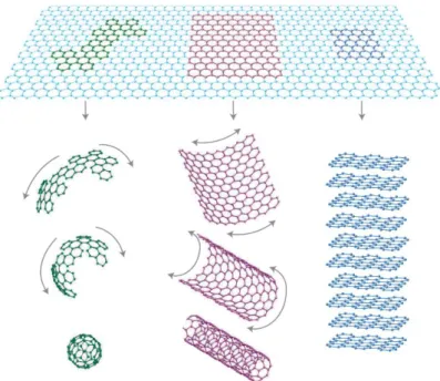
Graphene is the lastly discovered, and more interesting, allotropic form of carbon. It is the 2D basic constituent of other graphitic systems such as the 1D carbon nanotubes [94] and the 0D fullerenes [95] (Figure 1.20).
Figure 1.20 : Graphene (top) can be considered as the fundamental 2-dimensional form for all the graphitic
derivatives: the 0-dimensional fullerene (left), the 1-dimensional carbon nanotube (central) and the 3-dimensional graphite (right). From [96].
Although graphene properties have been investigated theoretically starting from the late 1940s [97–99], for decades its production in stable-form under ambient conditions was presumed impossible to obtain due to the so called Mermin-Wagner theorem [100,101] according to which long wavelength fluctuations destroy the long-range order for 2D crystals.
Despite the adverse theoretical background, stable graphene flakes was firstly isolated in 2004 by mechanical exfoliation of Highly-Ordered-Pyrolytic-Graphite (HOPG) by Geim and Novoselov [102], both awarded with Nobel Prize in 2010. Since then, the scientific community has seen a restless growth of published papers having graphene as main topic. This huge scientific attention is dragged since, as a material, graphene harbors some remarkable qualities. In the first place, graphene exhibits high electronic quality such that charge carriers can travel ballistically at micrometer scale at room temperature with charge carriers mobility as high as 2.5 × 105cm2V−1s−1 [103]. Moreover, graphene is able to sustain current densities of six order of magnitude higher than copper [104] while showing mesmerizing mechanical and thermal properties: a Young Modulus of 1TPa and intrinsic strength of 130 GPa have been observed [105], as well as a record high thermal conductivity in the range of 1500-5000 WmK-1 has been reported [106,107]. The 2-dimensional nature of graphene, furthermore, yields to wavelength-independent optical