Advances in semiconducting nanowires
for gas sensing: synthesis, device testing,
integration and electronic nose fabrication
Guillem Domènech Gil
Aquesta tesi doctoral està subjecta a la llicència Reconeixement 4.0. Espanya de Creative
Commons.
Esta tesis doctoral está sujeta a la licencia Reconocimiento 4.0. España de Creative
Commons.
nanowires for gas sensing: synthesis,
device testing, integration and
electronic nose fabrication
Guillem Domènech Gil
Director: Albert Romano Rodríguez
Departament d’Enginyeria Electrònica i Biomèdica
Institut de Nanociència i Nanotecnologia (IN
2UB)
nanowires for gas sensing: synthesis,
device testing, integration and
electronic nose fabrication
Memòria presentada per optar al grau de doctor
per la Universitat de Barcelona
Programa de doctorat en Nanociències
Autor
Guillem Domènech Gil
Director i tutor
Albert Romano Rodríguez
Departament d’Enginyeria Electrònica i Biomèdica
Institut de Nanociència i Nanotecnologia (IN
2UB)
Acknowledgements
First of all, I would like to thank my Ph.D. supervisor, Prof. Albert Romano Rodríguez for giving me the opportunity to participate in a research project for the first time, providing guidance and support during the work developed for more than 4 years, and for opening the path to new and exciting projects focused on nanoscience, always with enthusiasm and critical, but constructive, spirit.
I am also very grateful to have had the occasion of sharing parts of my research with Dr. Sven Barth and Dr. Paolo Pellegrino, who helped me to increase the quality of the work done during this thesis. I want to thank their support, their free transfer of knowledge and their ability in showing me key points for my research and career path, aspects that sometimes are missed among the scientific community.
I would also like to thank Dra. Isabel Gràcia and Dr. Carles Cané for providing the microhotplates and micromembranes, always with the best predisposition and open to new proposals.
I want to give thanks to the colleagues from the department who helped and supported me many times, giving a special mention to Jordi Samà, which whom I started my laboratory experience. Thanks also to my friends and labmates, Aïda Varea, Cristian Fàbrega, Olga Casals, Joan Daniel Prades, Xana Rodrígues, Omar Olmedo, Anna Batlle, Peter Pfeiffer, Montse Manadé, Xavi Arrese, Elena Aymerich, Alex Cabal, John Jaiber, Ismael Benito, Ismael Gabaldón, Christian Driau, Gerard Sánchez, Ferran, Carles and Qoumaruddin. I have spent many good times with them, inside and outside the laboratory, laughs and, of course, debates about science and, also, about completely different topics, what made my daily work easier and softer. I would also like to express my gratitude to Catalina, Julià, Lluis López, Adrià, Javi, Dani, Juan, Giovanni, Martí, Oriol Blàzquez, Mauricio Moreno, Romen Rodríguez and Sergi Hernández, who also helped me during these years when it was necessary and have spent many good times.
I would like to thank the moments shared with Irmina Peiró, Elena Aymerich, Paula Pirker, Aleksandra Adamczyk, Lily Walter and Alex Rodríguez, from who I also learned. It was really nice to help them in their works and get close to science together.
Sincere thanks to Alba, who stayed a long part of the thesis by my side, having lots of debates about chemistry that helped me considerably.
I have also to thank the strong support and encouraging that I received from Acadèmia Informa’t, Concepció, Núria, Jordi and all the teachers and students that shared these years and lectures with me.
Of course, this would not have been possible without spending time with my friends from outside the faculty. I thank them all the time they spent listening to explanations about my research, that was very amusing (for me), and for being there when it is necessary, to have a beer or to take a break. Thank you, Jordi, Rubi, Gerard, Laura, Bernat, Marta, Júlia, Charlie, Sabier, Enric, Silvia, Mar, Cayu, Andreu and Alicia May, I always have fun with you.
Finally, I would like to express my gratitude to my family, that with a lot of patience, always listen to me. Specially, to my parents, that are incredible referents each one, and to my brother from who I learn every day, overtaking our differences.
This work has been partially funded by the Spanish Ministry of Economy and Competitiveness, through projects TEC2013-48147-C6-1R (TEMIN-AIR) and TEC2016-79898-C6 (AEI/FEDER, EU).
Table of contents
1. Introduction ... 5
1.1 Solid-state gas sensors ... 6
1.2 Gas solid interactions ... 12
1.2.1 Physisorption and chemisorption ... 12
1.2.2 Adsorption isotherms ... 16
1.2.3 Chemoresistive gas sensors ... 20
1.2.4 Two-probe measurements with individual nanowires ... 23
1.3 Chemical vapor deposition ... 24
1.3.1 Vapor-liquid-solid mechanisms ... 24
1.3.2 Chemical vapor deposition ... 27
1.3.3 Carbothermal reduction ... 31
1.4 Integration methodologies ... 34
1.4.1 Microhotplates and micromembranes ... 34
1.4.2 Focused electron-ion beam induced deposition techniques ... 35
1.4.3 Electron lithography ... 37
1.4.4 Dielectrophoresis ... 39
1.4.5 Site-selective growth ... 41
1.5 References ... 43
2. Objectives ... 51
3. Individual semiconducting metal oxide nanowires for gas sensing ... 55
3.1 Gas sensor based on individual indium oxide nanowire ... 57
3.2 Gas sensor based on individual gallium oxide nanowire ... 69
4. Advanced integration methodologies for nanowire-based gas sensors... 105
4.1 Dielectrophoretic alignment of individual tungsten oxide nanowires for gas sensing ... 107
4.2 Gas sensor based on individual tin oxide nanowire contacted by Electron Beam Lithography ... 125
5.1 Site-selective growth and In-situ integration of different nanowire material for
Electronic-nose applications ... 139
6. Conclusions and future work ... 163
6.1 General conclusions ... 163
6.2 Specific conclusions ... 164
6.3 Future work ... 167
7. Resum en català ... 171
“If I have an apple and you have an apple and we exchange them, then both still have one apple. If I have an idea and you have an idea and we exchange them, then both will have two ideas.” George Bernard Shaw
1. Introduction
In the last two decades nanotechnology has given rise to a scientific and technical revolution, contributing with novel research paths and applications, which has generated huge interests among the scientific community and industry. As a consequence, around the world, there have been important investments in this field with the aim of leveraging new products and commercial opportunities. In fact, nanotechnology has been declared to be the technology of the twenty-first century and only time will tell if this statement will turn out to be true.
Nanotechnology is the technology suitable to provide tools to manipulate matter at the nanometer scale, meaning 1 to 100 nm at least in one of the material dimensions. Not only the scale is important, as miniaturization along Moore’s law curve is nowadays a routine in the microelectronic industry, but also to exploit the new properties arising from nanoscale effects [1,2]. Nanotechnology is now understood as a broad-base multidisciplinary field forecasted to reach mass use by 2020 and to revolutionize many aspects of human life [2]. Nowadays, new instrumentation and methods have allowed femtosecond measurements with atomic precision [3], single-phonon spectroscopy [4] and sub-nanometer resolution morphological measurements [5], single-atom [6] and single-molecule characterizations [7], simulations of large assemblies of atoms or crystalline structures [8]; the discovery and development of important new phenomena such as plasmonics [9], negative index refraction in IR/visible wavelength radiation [10], precision measurements of the Casimir forces [11], teleportation of information between atoms [12] which could enable quantum computing, biointeractions at the nanoscale [13] or fabrication of graphene [14], among others. Therefore, even being a technology under development that still lacks some required tools and with misconceptions in some
fundamental areas, since its invention all the mentioned achievements point out the potentiality of nanotechnology.
Parallel to this fact, the concern about toxic and harmful gases for human health has been increasing during the last two centuries. This is due to our life style, in which large amounts of gases are propagated either in open air or in indoor environments. This is especially true in the last decades. The presence of toxic gases and pollutants is the first environmental cause of premature death in European Union, with 400.000 premature deaths per year [15,16]. Since the fabrication of the first device intended to sense flammable gases in coal mines in 1816 [17], the fire-damp, warning the lack of oxygen and the excess of methane, an enormous variety of gas sensors have been developed [18], driven by the ever-growing concern of the citizens about such effects.
Gas sensors are transduction devices that transform chemical and/or physical information effects of the presence of a certain gas into an electrical signal, whose value can be measured. In this way, the concentration of gaseous species in the vicinity of the sensors can be surveyed and, if the gases are harmful, the sensor can help preventing dangerous situations by allowing the control of the gas emitting sources.
The gas sensor market was valued at 1.67 billion € in 2017 and it is estimated to grow significantly from 2025 [19]. Gas sensors are adopted for several applications, such as medical, industrial, petrochemical, automotive manufacturing industries, food process, building and domestic appliances or quality control [19].
1.1 Solid-state gas sensors
Solid-state gas sensors are devices based on the change of the physical and/or chemical properties of their sensing materials when exposed to different gas atmospheres. Depending on the sensing material, these properties can be tuned to a certain extent, adapting the fabricated gas sensors to different needs. In this sense, nanotechnology contributes with numerous tools to study in depth the prevailing materials used in gas sensing, unwrapping novel effects occurring in nanostructured materials.
The tremendous variety of solid-state gas sensors available nowadays can be sorted in groups as a function of the transduction mechanism taking place at the sensing material.
This gives rise to optical, mass-sensitive, calorimetric or conductometric gas sensors, among others, which will be briefly described in this section. A section specially devoted to the evolution, advantages, drawbacks and general trends of semiconducting metal oxide-based (MOX) gas sensors, a type of conductometric gas sensors, is presented in this work, as prototypes of MOX-based gas sensor are developed, fabricated and characterized in this thesis.
Optical gas sensors transform the interactions between the gas and the sensing material into changes in the electromagnetic radiation propagation [20]. This effect can be directly related with physical or chemical changes of the target molecule or, for analytes that do not produce optical changes, of a label marker [21]. In general, this kind of sensor presents high selectivity towards particular gaseous compounds, allowing to detect a specific gas in these mixtures. However, they lack portability due to fragile optical components, difficulties in miniaturization and are quite expensive [18]. Figure 1
a) shows a schematic diagram of one of this type of devices, namely a surface plasmon
resonance-based sensor.
Mass-sensitive gas sensors are based on the mass changes occurring at the material’s sensing surface during the interaction with gaseous species. Examples of sensors using this basic principle are microcantilevers [22,23], shown in Figure 1 b), surface acoustic wave [24] or quartz crystal microbalance sensors [25]. In general, these sensors present fast and high responses to the surrounding gases,but their behavior depends considerably on temperature and humidity, apart from needing complex electronic circuits to operate. Calorimetric gas sensors are based on the temperature variation produced by a gas on certain materials, which will be later measured as resistance variation. In this case, the detecting elements consist of small “pellets” of catalyst-loaded ceramics whose resistance
Figure 1: (a) Schematic diagram of surface plasmon resonance-based sensor (reprinted from Ref. [21]) and (b) schematic representation of microcantilever and the transverse deflection (reprinted from Ref. [23]).
changes according to the surrounding gas species [26]. The term pellistor is used to designate this type of sensors, combining the words pellet and resistor.
Among the conductometric gas sensors, one of the most extended sensing materials are the semiconducting MOX. These materials are used to transduce the chemical reactions occurring at their surface with the surrounding gas, such as reduction, oxidation, adsorption or other surface reactions between adsorbed species, into reversible and measurable electrical resistance variation, which are used to extract the concentration of the different gases present in the ambient near the sensor.
The first written evidence regarding the idea of using the changes in conductivity/resistivity of a MOX under the presence of gases dates back to 1959 in a work by Mollwo and Heiland [27], who studied the conductivity changes of ZnO when kept under vacuum at temperatures up to 600 ºC and, simultaneously, exposed to oxygen and hydrogen. The first practical gas sensor based on a semiconductor MOX was proposed in Japan in 1962 by Seiyama [28], and shortly afterwards by Taguchi [29], using as sensing element films of ZnO and SnO2, respectively. Taguchi founded Figaro
Engineer Inc. in 1967, which is a worldwide company that still supplies gas sensors based on MOX all around the globe. During the next few years, the use of SnO2-based gas
sensors started to spread in Japan, while other types of metal oxides were simultaneously investigated [30], as shown in Table 1. Seiyama and co-workers studied the selectivity and sensitivity of MOXs, as well as their modifications using noble metals [31], gaining a large amount of information on the behavior of different metal oxide materials, which has strongly impacted the sensor fabrication field. However, the understanding of the sensing mechanisms and kinetics are still incomplete, due to complicated crossed effects, such as surface defects, surface adsorption properties, metal-semiconductor junctions or MOX particle size influence.
Year Material Gas detected Researcher
1962 ZnO (thin film) H2, Alcohol Seiyama, et. al. [28]
SnO2 Combustible gas Taguchi [29]
1963 SnO2 + Pd, Pt, Ag. Combustible gas Taguchi [32]
1966 ZnO, SnO2 Reducing gas Seiyama, et. al. [33]
SnO2 + Al2O3 Combustible gas Taguchi [34]
In2O3+ Pt H2, Hydrocarbon Loh [36]
1969 SnO2 + SiO2 Combustible gas Taguchi [37]
1971 ZnO + Pt + Ga2O3 CH4, NH3 Bott, et. al. [38]
1972 SnO2 + Pd Propane Seiyama, et. al. [39]
Table 1: summary of key solid-state gas sensor publications during the decade 1962-1972.
To understand the behavior of MOX as gas sensors, detailed studies measuring simultaneously the resistance change of the sensing material and the gas species adsorption are essential. For this purpose, two different set-ups are generally used: under clean, dry and ultrahigh-vacuum conditions or/and at pressures and temperatures mimicking real ambient conditions [40]. The experimental methodology was established in the course of more than 50 years [41], with a first systematic approach formulated in 1985 in a series of papers entitled “Development of chemical sensors: empirical art or systematic approach?” collected in a book [40]. Up to that moment, several techniques were already applied to investigate the gas adsorption, such as electron paramagnetic resonance (EPR) for investigations of oxygen adsorption [42] or infrared spectroscopy (IR) for CO adsorption studies [43]. The mentioned systematic approach pushed forward the basic understanding of the chemical reactions occurring at the surface of the sensing material and the corresponding conduction mechanisms. An example of this is the exhaustive study of SnO2 surface reactions when exposed to acetic acid, methane and CO,
published in 1989 [44]. By the end of the 90s, different spectroscopic methodologies were applied for sensors operating under ideal or under in situ real operation conditions. As shown in Figure 2. This fact led, in the early 2000, to the definition of in situ and operando spectroscopic techniques [45]:
• In situ spectroscopy: spectroscopic characterization of sensing material under
operation conditions or conditions relevant to operation; herein, the sensing performance of this material may be not characterized or may be characterized in a separate experiment.
• Operando spectroscopy: spectroscopic characterization of an active sensing
element in real time and under operating conditions with the simultaneous read-out of the sensor activity and monitoring of gas composition.
The operando spectroscopy couples the electrical and spectroscopic techniques with the aim of correlating the sensor activity with the gas composition of its surroundings. If these techniques are applied under real ambient conditions, then the study can elucidate and predict how a sensing material will behave when exposed to a non-controlled ambient that combines gases or gas mixtures whose interaction are already known.
With the appearance of nanomaterials, a new scenario was presented, with morphologies giving rise to a much larger surface-to-volume ratio compared to thin film materials, which is expected to give rise to an increase of the sensor sensitivity. The use of nanoparticles (NP) of metal oxides was the first choice and extensive work was carried out in the 90s and early 2000s to fabricate high crystalline quality and nanometre-sized NPs for their use in gas sensors. However, the difficulty in fulfilling both requirements simultaneously, as improving crystalline quality required high temperature treatments, which resulted to increase in nanomaterial size, limited this improvement path.
Nanowires (NWs) were considered for gas nanosensor fabrication at a later point, as their surface-to-volume ratio is lower than that of NPs, but with higher crystallinity and stability at elevated temperatures. The first proposal of a MOX gas sensor containing nanowires (NWs) as a sensing element was published by Kolmakov et al. in 2003 in California [46] using SnO2 NWs to detect CO and O2. One year later, a study on ZnO
NWs working as ethanol sensors [47] was presented in China. The amount of chemical reactions that are continuously taking place at the surface of the sensing material are directly related with the total available surface adsorption sites. Nowadays, NWs are being incorporated as active material in many different gas sensing approaches, and with several surface treatments, with the aim of enhancing their intrinsic properties, as for example individual NWs [48] and/or decorated with novel metal nanoparticles [49] or using other MOX, such as WO3 [50], TiO2, CeO2, Ga2O3 [51], etc.. These possibilities
were the starting point for the fabrication of gas sensors developed in this PhD thesis dissertation.
Working with MOX as sensing material has several advantages, such as simplicity in device configuration (especially for chemoresistors) and relatively high reliability, low cost of fabrication, robustness, long operating time and reasonable baseline drift, even in the presence of corrosive gases or when aging occurs, as well as the fact that the sensors respond to a wide variety of gases. However, the sensors generally lack selectivity, require the development of practical integration methodologies, use considerable electrical power to operate and require long stabilization times [40].
The electronic-nose configuration (e-nose) appeared to solve the lack of selectivity of the gas sensors, employing them as an olfactory system in a smell assessment instrument, mimicking the human nose but trying to overcome its natural limitations, like non-quantified results, tiring or subjectivity [52]. To promote this technology, MOX-based gas sensors became ideal candidates in areas such as food and automobile industry or indoor and environmental air monitoring. An e-nose is, according to the accepted definition, a device that comprises an array of heterogeneous gas sensors and a pattern
recognition system [53]. The heterogeneity can arise either from a combination of
different types of sensors, different materials or the same material operating at different conditions, generally, at different temperatures. Nowadays, several e-noses are commercially available in the market (i-Pen, PEN2, QCS, Artinose, FF2, Promethus, Aromascan A32S, Cyranose 320, etc. [52]), mainly based on metal oxide semiconducting materials, for generic purposes and suitable for a broad range of applications. The e-nose field is still unripe, but with time it could become the strategy to overcome the selectivity problem of most of the gas sensors, being able to discriminate among different gases in a complex atmosphere.
To fabricate MOX-based gas sensors, the general procedure includes the synthesis of the MOX sensing material on a specific substrate, followed by the transfer and integration of this material in the final architecture of the sensing device. The implementation of this procedure occurs with different difficulties due to the various technological steps required. To reduce the fabrication steps, the site-selective growth and in-situ integration of the sensing material in the final device has been proposed in some recent works of our research group [54]. This strategy joins the material fabrication and the integration in the final device and, consequently, reduces the technological steps involved in the whole process, increasing its robustness and decreasing the expected cost per unit, shading some light to the lack of practical methodologies for material integration.
From all this it is clear that a breakthrough could be achieved in the new generation of MOX-based gas sensor prototypes by combining the different mentioned strategies in a single system: using NWs to enhance the sensitivity of the sensors, simplifying the fabrication, increasing the robustness and reducing the cost by employing the sitselective growth and in-situ integration of NWs and increasing the selectivity via the e-nose configuration.
1.2 Gas solid interactions
The basic processes occurring at the surface of MOX sensing materials, involving chemical and physical reactions that are later transduced into an electrical signal and used to monitor the presence of different gas species around the sensor, are described in this section. The first part presents the different types of categorized adsorption situations that can take place between a gas atom or molecule and the surface of a solid material. Next, a general description of the adsorption processes occurring is presented and discussed. Finally, the events that lead to the conductance variations measured in gas sensing are described.
1.2.1 Physisorption and chemisorption
The adsorption process is the first step of the gas sensing mechanism. By definition, adsorption is an increase in the concentration of a dissolved substance at the interface between condensed and gaseous phases due to the effect of surface forces. To study the adhesion of a gas molecules (adsorbate) on a solid surface (adsorbent), the Hertz-Knudsen equation can be used as a mathematical description of the flux of molecules (𝜙𝑖) reaching
a surface [55]:
𝜙
𝑖=
𝑝(2𝜋𝑚𝑘𝐵𝑇)1 2⁄ (1)
where p denotes the pressure, m is the mass of the molecule, 𝑘𝐵, the Boltzmann constant and T, the temperature. This equation shows that the gas molecules adsorption on an adsorbent is a process highly dependent on the temperature, pressure and adsorbate mass. In addition, and not in appearing in Equation 1 as they show complex dependencies,
affect the adsorption. This gives rise to non-linear dependencies of adsorption with these latter parameters, which makes it difficult to understand and model the gas molecule adsorption processes. After being adsorbed, the adsorbate can be desorbed, a process that typically requires energy to occur, because the adsorption brings the adsorbate to a state of lower energy. Desorption is defined as the reverse process to adsorption and can be, for example, thermally promoted. The basic principle of the MOX-based gas sensors is the measurement of an electrical signal as a result of the charge carrier transfer between the MOX and the adsorbed and/or desorbed gas molecules. When a steady state between adsorption and desorption is achieved, the electrical signal to this particular gas mixture is constant.
In general, two types of adsorption situations are considered: physical or chemical, called physisorption and chemisorption, respectively. Usually, the difference between physisorption and chemisorption lies in the forces retaining the adsorbate on the adsorbent, inducing or not a chemical bonding arrangement and a charge transfer. In the case of physisorption, all the gas species in the surroundings of the material tend to be adsorbed as the result of Van der Waal forces: London, Debye and/or Keesom. In general, the process is reversible, non-dissociative, the adsorbate remains unmodified and occurs at temperatures close to the boiling point of the adsorbate [59]. At higher temperatures the chemisorption, occurring with charge transfer between the adsorbate and the surface of the material, dominates. However, it is not clear which is the exact limit of charge transfer or energy involved to distinguish between chemical and physical adsorption [59], which makes the line separating both phenomena a controversial issue. Additionally, there could exist intermediate states, as for example, some authors propose to differentiate between strong and weak chemisorption [59].
It is generally accepted that the physisorption can be described as a combination of potential energies from the long-range attractive polarization potential and the Pauli repulsion for electrons, binding an atom or a molecule to a solid surface [60,61]. Lennard-Jones proposed a simple formula to depict both interactions by a unique potential [62]:
𝑉
𝑝ℎ𝑦𝑠(𝑟) = 4𝜀 [(
𝜎𝑟)
12− (
𝜎𝑟)
6]
(2) where 𝜀 is the depth of the potential, 𝜎, the distance at which the potential is zero and 𝑟, the distance from the surface. Thus, Van der Waals forces induce a long-rangeinteraction that, independently of the gas specie, attracts the adsorbate to minimize its energy at a distance of r > 0.3 nm, involving few hundreds of meV [63]. The small energy involved in this process makes the adsorbate molecules easily mobile on the surface and, thus, can be rapidly desorbed.
In the case of chemisorption, there is a reorganization of the electrons from the adsorbate and from the solid adsorbent. During the adsorption process, the energies involved are of the order of the chemical bonds of the gas molecule, which can lead to the formation of new bonds and breaking of existing ones. The process is dissociative (the molecules break down into smaller molecules or individual atoms), can be localized in a specific site and is irreversible for some molecules [63]. In addition, chemisorption is not as temperature restricted as physisorption. However, its relevant effects for gas sensing purposes are related to a specific range of temperatures. At low temperatures the mechanism barely occurs, being extremely slow in contrast to physisorption, which dominates. In general definitions, the equilibrium distance for chemisorption is usually found to be between 0.1 and 0.3 nm [64] and the energy involved in chemisorption processes are around several eV. Even though there exist some key points that are different for physisorption and chemisorption, there is not a clear barrier that separates them in temperature or pressure.
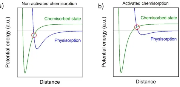
For chemisorption, the potential energy can be mathematically described using the Lennard-Jones, the Morse or the Buckingham potentials [64]. The Lennard-Jones
Figure 3: Potential energy in a) a non-activated chemisorption and b) an activated chemisorption process. The activated chemisorption requires additional energy of the adsorbate in order to pass from the physisorbed to the
chemisorbed state.
potential is represented as a function of the distance from the surface of the solid material in Figure 3 a) and b) for a non-activated and an activated process, respectively. The difference between both lies in whether the crossing point of the physisorption and chemisorption potential energies occurs at a positive or negative energy value. When a gas molecule or atom approaches the surface, it first experiences the Van der Waals interaction, like in a physisorption process. As it comes closer to the surface, the chemisorption potential starts to become important.
In a non-activated chemisorption situation, the adsorbate can reach the chemisorbed state almost straightforward, without activation energy. For the activated chemisorption, the meeting point of potentials occurs at positive energies. As a consequence, if the molecule or atom has enough energy when approaching the surface, the gas specie will overcome this energy barrier and adopt its lower energy state, following the chemisorption potential curve.
For chemisorption, the activation energy can be understood to represent the energy necessary for the dissociation of a molecule, which can be described as an Arrenhius-like process [65] and, thus, temperature dependant:
𝑘
𝑝= 𝐴𝑒
−𝐸𝑝⁄𝑘𝐵𝑇 (3)where 𝑘𝑝 denotes the reaction rate constant, 𝐴 is the pre-exponential factor, 𝐸𝑝,
the activation energy of the process, 𝑘𝐵, the Boltzmann constant and 𝑇, the temperature.
Equation 3 applies both to activated and non-activated processes. Desorption is also a
process that requires to overcome an energy barrier to occur. For this reason, the activation energy 𝐸𝑝 can be referred to 𝐸𝑎𝑑𝑠 or 𝐸𝑑𝑒𝑠 , depending on whether the study is focused on adsorption or desorption.
Summarizing the adsorption and desorption events that can occur when a gas molecule interacts with a clean solid surface could be:
1. The gas molecule is elastically scattered without any loss of energy, giving rise to no adsorption or desorption.
2. The gas molecule is inelastically scattered: being physisorbed, when impinging with low energies, or chemisorbed, for high enough energies.
3. If the gas molecule is physisorbed, it can be later (a) desorbed, being scattered back to the gas phase, (b) diffused to a neighbour site or (c) chemisorbed. 4. If the gas molecule is chemisorbed it can afterwards (a) release chemical
energy to the solid and become localized at the adsorption site, (b) lose chemical energy and dissipate the excess of energy by diffusion or (c) be desorbed.
The main differences between physisorption and chemisorption can be summarized as follow:
Physisorption Chemisorption
Weak and long-range interaction Strong and short-range interaction
No surface reaction Surface reactions
Non-site specific Site localized
Energy range: meV Energy range: eV
Table 2: Comparison between the main characteristics of physisorption and chemisorption.
1.2.2 Adsorption isotherms
The statistical description of the adsorption processes occurring on a solid surface of a monoatomic gas at a constant temperature is a problem described by several models, called adsorption isotherms. The study of the different adsorption mechanisms is key to understand the processes occurring at the surface of the studied sensing materials. These adsorption processes can be interpreted using various isotherm models, such as the Langmuir [59], Freundlich [66] or Brunauer, Emmett and Teller (BET) [67] isotherms. The isotherms help to understand the interaction between the solid surface and the gas molecules in a steady state of adsorption, shading light to the dynamics of the system. The adsorption isotherms reveal the amount of gas molecules adsorbed on a solid surface given certain conditions of pressure and temperature.
The Langmuir isotherm is a simple and ideal model that is based on several assumptions:
1. There is only monolayer adsorption 2. There are limited adsorption sites
3. All sites have the same adsorption probability 4. There is no interaction between adsorbed molecules
With these assumptions, the Langmuir isotherm equation can be derived from gas kinetics theory [59], describing the adsorption and desorption ratio in the steady state, as:
𝜃 =
𝑏𝑃𝑥1+𝑏𝑃𝑥 (4)
where 𝑃𝑥 is the adsorbate partial pressure, 𝑏 is a parameter that depends on the adsorbate, the adsorbent and the temperature, and 𝜃 is the normalized surface coverage. The latter is the ratio between the adsorbed molecules (𝑁) and the total number of available sites (𝑁∗):
𝜃 =
𝑁𝑁∗ (5) In more detail, the parameter 𝑏 in Equation 4 is defined as:𝑏 =
𝑠𝑘0𝜈√2𝜋𝑚𝑘𝐵𝑇
𝑒
( 𝑄
𝑘𝐵𝑇) (6)
where 𝑠 is the effective surface area, 𝑘0 is the sticking probability, 𝜈, the oscillation frequency of adsorbed molecules, 𝑄, the adsorption heat (𝑄 = 𝐸𝑑𝑒𝑠− 𝐸𝑎𝑏𝑠) and m is the mass of a single molecule. The effective surface area is defined as a geometrical controlling factor for a chemical reaction. It is not uniquely determined for every specific material, but it also depends on the type of chemical reaction, the state of agglomeration and on the compactness of the agglomerates.
This model defines isotherm type I, shown in Figure 4, suitable for ultraclean, well-ordered surfaces interacting with small-molecule adsorbates, but oversimplified to
correctly describe real-word scenarios [67]. From this isotherm, it can be observed that at low pressures the coverage is proportional to the equilibrium pressure of the gas, while at high pressures, it tends asymptotically to 1. Apart from offering a first approach to understand the adsorption process, this model is the basis of most of the adsorption theory. Other adsorption models treat the first adsorbed monolayer as described by the Langmuir model, adding further terms to describe the adsorption of subsequent layers. Furthermore, the surface coverage can be also related to the sensor response in a complicated manner [69]:
𝑆 ∝ 𝜃(𝑃, 𝑇)
(7)
The BET isotherms establish different relations between the equilibrium and saturation pressures, 𝑝 and 𝑝0 respectively, and the adsorbate surface coverage, extending the Langmuir theory to multilayer adsorption. Such surface coverage can be determined from following relation [67,69]:
𝜃(𝑃, 𝑇) =
𝑝 𝑝⁄ 01−𝑝 𝑝⁄ 0
𝑏𝐵𝐸𝑇(𝑇)
[1+𝑝 𝑝⁄ (𝑏0 𝐵𝐸𝑇(𝑇)−1)] (8)
where 𝑏𝐵𝐸𝑇(𝑇) stands for the BET constant:
Figure 4: Classification of typical adsorption isotherms (I-V) showing vapor adsorption as a function of relative pressure p/po (reprinted from Ref. [66]).
𝑏
𝐵𝐸𝑇(𝑇) = exp [
𝜀1−𝜀𝑙𝑓𝑘𝐵𝑇
]
(9)and where 𝜀1 and 𝜀𝑙𝑓 are two energy parameters that measure the strength of adsorption of the first monolayer at the surface and in each following monolayer of adsorbate, respectively. Multilayer adsorption can occur when 𝜀1 > 𝜀𝑙𝑓. Isotherm type II and III can be modeled using the BET equation. The difference in the shape between these two isotherms results from the differences in the strength of the adsorbate-adsorbent interaction [67]. Isotherms types IV and V are characteristic of adsorption processes on mesoporous solids via multilayer adsorption, followed by capillary condensation. They can be described using a combination of the BET model and a second model that accounts for capillary condensation in small pores or capillaries [67] or with special treatments on BET theory [70]. Isotherm type IV is an intermediate case between I and III, where the adsorbed number of molecules per site is finite. Isotherm type V is similar to type II and the difference comes from the processes followed at low pressures after adsorption: in the isotherm type V case multianchorage occurs and, while for isotherm type II, a dimerization process takes place. Type V is typically obtained in carbon-based materials interacting with water vapor [71,72].
To model even more realistic situations, in addition to the postulates of the Langmuir model, the assumption of molecule dissociation can be made. This approach, the so-called dissociative Langmuir model, is satisfactorily used to describe the adsorption process of dissociated oxygen atoms at MOX surfaces [73]. The model assumes that the gas molecule is formed by 𝑚 atoms and that it dissociates into 𝑛 parts as a result of the adsorption. Assuming only a dissociation into 2 parts (order 2), the formula for the surface coverage results in:
𝜃 =
(𝑏𝑃𝑥)1 2⁄1+(𝑏𝑃𝑥)1 2⁄ (10)
This equation can be used for the theoretical study of semiconductor gas sensors. Via numerical simulations, the response of the sensor towards individual gas species can be quantitively modeled, studying the effects of parameters such as the operating temperature or the doping level on the sensor response. It is worth to mention that the Freundlich isotherm [74], proposed as an empirical relation before the appearance of the
Langmuir model, can also be used for semiconducting gas sensors, and is formulated as follows:
𝜃 = 𝑎𝑃
𝑥1 𝑛⁄ (11) where 𝑛 is a constant value always < 1. The particularity of the Freundlich model is that it assumes an exponential decay in the heat of adsorption with increasing coverage that the Langmuir model does not account for [67], which results in a better fitting to a real-world scenario.1.2.3 Chemoresistive gas sensors
This section is devoted to the mechanisms that, after the adsorption of a gas atom or molecule at the surface of a solid semiconducting MOX, produce the variations in the sensor signal due to charge transfer between the gas species and the sensing material.
When a gas molecule is adsorbed at the surface of a solid, electrons can be captured by this molecule or electrons from the molecule can be transferred to the solid [75,76]. This is possible if the lowest unoccupied orbital of the molecule is located below the Fermi level of the solid (acceptor levels) or if the highest occupied orbital from the adsorbate is above the Fermi level of the solid (donor levels). When one of these two situations occur, a net charge is fixed at the surface of the solid, giving rise to an electric
Figure 5: Energy band diagram of an n-type metal oxide semiconductor, where an adsorbate at the surface creates an acceptor level, which produces an upward band bending (adapted from Ref. [79]).
field inside the semiconductors, that causes energy band bending in the material. For example, if the semiconductor donates one electron to the adsorbed molecule, this gives rise to the accumulation of negative charge at the surface, as shown in Figure 5, and produces an upward bending of the band diagram close to the surface. Assuming a n-type semiconductor with a Fermi level within the bandgap and close to the conduction band, the band bending produces a reduction of the majority charge carrier density (electrons) and close to the surface and gives rise to an electron depletion layer, which contains fixed positive charge that compensates the negative surface charge at the surface. The change in the density of charge carriers at the depletion layer produces conductivity variations in the semiconductor, leading to a resistance change, in this example, a reduction. The conductivity variation can be described as:
∆𝜎 = 𝑒[𝜇
𝑛∫ 𝑛(𝑧) − 𝑛
𝑏𝑢𝑙𝑘𝑑𝑧 + 𝜇
𝑝∫ 𝑝(𝑧) − 𝑝
𝑏𝑢𝑙𝑘𝑑𝑧]
(12)where 𝑛 states for the density of electrons, 𝑝, for that of holes and 𝜇𝑛 and 𝜇𝑝 are the electron and hole mobilities, respectively.
Combining the chemical adsorption formalism and the semiconductor physics calculations, the so-called power law for the resistance of a semiconducting gas sensors is proposed:
𝑅 = 𝑎𝑃
𝑛 (13)where a is a constant and the value of 𝑛 depends on the morphology, the bulk properties of the sensing material and the dissociation mechanism. The relation described in Equation 13 is supported by experiments [77]. Regarding the geometry of the sensing material, it is worth mentioning that it acquires special relevance, since, theoretically, the full depletion of the semiconductor metal oxide could be reached. This fact is expected to greatly enhance the response of the sensors. From these observations, it is evident that the surface-to-volume ratio and geometry of the sensing material are important factors influencing the conductivity and, consequently, the response of the sensor.
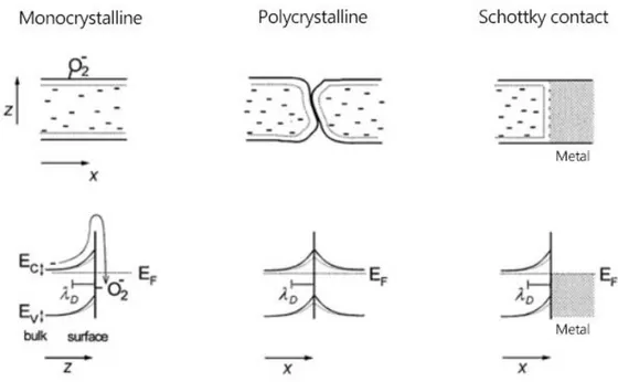
Regarding the crystallinity of the sensing material, polycrystalline materials present different behavior than their monocrystalline counterparts, for which only the surface is supposed to be contributing to the gas sensing properties. The presence of grain boundaries in polycrystalline materials produces multiple Schottky barriers and, according to the previous reasoning, different space charge region depletions are induced
between the individual grains, thus, contributing to the change in the resistance of the material and modifying the effect of the adsorbed gas molecules in an uncontrolled manner. Furthermore, it is expected that the diffusion of the adsorbed molecules along the surface of a polycrystalline material is slower than in a monocrystalline material and, therefore, the response time of the final devices is generally longer. At the junction of the semiconductor and the metal electrodes, commonly used to contact the sensing materials, also a Schottky barrier may be found. When gas adsorption takes place, the height of this barrier may be modified, producing resistance variations in the sensing device. A sketch of these processes is depicted in Figure 6.
The response of the sensors towards the different adsorbing species is defined in this work as the relative change in the sensor’s resistance, irrespective from oxidizing or reducing gases or p- or n-type semiconductors, as:
𝑆 = 𝑅𝑒𝑠𝑝𝑜𝑛𝑠𝑒 (%) =
|𝑅𝑎𝑖𝑟−𝑅𝑔𝑎𝑠|𝑅𝑎𝑖𝑟 (14)
The sensor’s response time (𝜏𝑟𝑒𝑠𝑝) is here defined as the time span between 10 and 90 % of the steady state resistance after the exposure of a certain constant gaseous concentration. In a similar way, the recovery time (𝜏𝑟𝑒𝑐) is the time span between the gas
Figure 6: Energy band diagrams of three different scenarios where the adsorption of gas leads to band bending, affecting the conductivity of the semiconductor material: monocrystalline, polycrystalline material, which is represented by a grain boundary, and a Schottky contact, formed by the junction of a metal and a semiconductor
timulus is interrupted and the resistance changes from the 10 to the 90 % of the interval between the steady state and the base resistances.
1.2.4 Two-probe measurements with individual nanowires
For a precise determination of the free charge carriers in the semiconducting material, the use of four electrical contacts to the material is the preferred configuration, as it allows performing four-probe measurements, which allows minimizing the contact resistance between the metal and the semiconductor. However, to simplify the electrical circuits required for the device readout and to decrease the time and cost of fabrication, two contacts are generally used. Using this configuration, in direct current measurements, the voltage drop measured when applying a fixed current is the sum of the contributions of the voltage drop at the resistance corresponding to the NW (𝑅𝑁𝑊) and that corresponding to the contacts or the Schottky interface (𝑅𝑆𝐼). The overall resistance measure, R, is given by:
𝑅 = 𝑅
𝑁𝑊+ 𝑅
𝑆𝐼 (15) It is important to know which is the relative contribution of each of these 2 terms, because it is difficult to discriminate which is the one that changes most in the presence of gas in the sensor’s environment. It is well-known that a Schottky barrier is fabricated when depositing Pt contacts to a MOX NW, due to the difference in the metal work function and the electron affinity of the semiconducting NW [78-80]. A Schottky barrier acts as a potential barrier at the interface between both materials. This effect can be observed as a nonlinear behavior in the current-voltage (I-V) characteristics when measuring at room temperature and can be explained interpreting the system as a two back-to-back Schottky barriers connected in series at the ends of the NW [78]. In the present work, however, the experimental conditions are such that the contribution of the Schottky barrier in the total resistance is low and, thus, we will be measuring mostly the contribution of the NWs.1.3 Chemical vapor deposition
1.3.1 Vapor-liquid-solid mechanisms
Whiskers, the first name that the NWs received when they were first reported, were observed in natural ores in 1500s. The concept of growth is commonly used to describe the formation of whiskers or NWs. This concept was adopted in 1600s because the silver whiskers from the rocks seemed to grow like grass [81]. In the 1950s, intensive research in the Bell Telephone Laboratories led to the growth of whiskers of several materials including B, B4C, Al2O3, SiC, and Si3N4 [81]. The main objective of these
studies was a reinforcement additive to be introduced in metals and plastics.
In the mid 1960’s, Wagner and Ellis from the Bell Laboratories, first proposed the vapor-liquid-solid (VLS) mechanism in a series of publications [82-84] focused on silicon whiskers growth. These publications elucidated how the whiskers growth proceeded, stating, among other things, that: (a) an impurity is essential for whisker growth and (b) a small globule is present at the tip of the whisker during the growth [82]. Nowadays, the “impurity” is commonly known as catalyst in the NW literature (possibly a misleading term in this context) and the globule is used as the logical demonstration of the occurrence of the VLS mechanism.
In the VLS mechanism it is proposed, as initial scenario, that the catalyst forms a liquid alloy droplet with the substrates, while the material that will later form the whisker
Figure 7: Schematic illustration of the VLS mechanism as proposed by R.S. Wagner (reprinted from Ref. [82]).
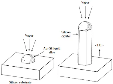
is in the gas phase. This situation transforms the catalyst into the preferred deposition site for the vapor phase material on the substrate, as shown in Figure 7 from ref. [83]. The next step occurs at the vapor-liquid interface, where material from the vapor phase is transferred directly into the liquid droplet. This ends up causing the supersaturation of the liquid alloy droplet and the precipitation of material at the liquid-solid interface [83]. At the correct temperature and pressure, this produces a precipitation in solid form whose growth is guided by the catalyst.
It is clear that the catalyst plays a key role in the VLS mechanism and there is a list of criteria that should be considered at the moment of its choice [85]:
1. It must form an alloy or liquid solution with the crystalline material that is attempted to be grown.
2. The distribution coefficient of the catalyst, defined as 𝐾𝑑 = 𝐶𝑠⁄ , must be𝐶𝑙
less than 1 (where 𝐶𝑠 and 𝐶𝑙 are the solubilities in the solid and liquid phases,
respectively).
3. The equilibrium vapor pressure of the catalyst around the liquid alloy must be small, since evaporation would otherwise change the droplet volume, leading to changes in whisker size during the process.
4. The catalyst must be inert to the byproducts of the chemical reactions that generates the vapor source.
5. The interfacial energies of vapor-solid, vapor-liquid, and liquid-solid systems and the resulting wetting characteristics determine the shape of the growing crystal. A large contact angle is necessary for the formation of whiskers. 6. In growing whiskers of compound materials, the catalyst can be the excess of
one of the materials to be grown.
7. The choice of the catalyst and the growth temperature must avoid the formation of an intermediate solid phase constituted by the catalyst and one of the vapor phase materials.
8. To obtain unidirectional growth, the solid-liquid interface must have well-defined crystallographic features.
The importance of the catalyst arises also from the fact that the droplet beads control the diameter and morphology of the grown material. Wagner suggested that there
is a minimum diameter determined by the stability of a liquid droplet in its own vapor [85]:
𝑟
𝑚𝑖𝑛=
2𝜎𝐿𝑉𝑉𝐿𝑅𝑇𝑙𝑛𝜎 (16)
where 𝑟𝑚𝑖𝑛 is referred to the minimum critical radius of a whisker, 𝜎𝐿𝑉, the liquid-vapor interfacial energy, 𝑉𝐿, the liquid molar volume, 𝑅, is the ideal gas constant, 𝑇, the temperature, 𝑙𝑛 is the napierian logarithm and 𝜎 the degree of saturation, given by:
𝜎 =
𝑃−𝑃𝑒𝑞𝑃𝑒𝑞 (17)
where 𝑃 and 𝑃𝑒𝑞, are the actual and the equilibrium vapor pressures, respectively.
These expressions, that can be used as a general guideline, link the growth conditions and intrinsic properties of the studied materials to the final whisker morphology. Wagner, and later Givargizov, gave large evidence that the growth temperature determines the growth rate, diameter and stability of the whiskers. In the studies of Givargizov one can find the fitting of his data to growth rate, that gave rise to the following expression [86]:
𝑉 = 𝑏
(∆𝜇)2𝑘𝑇 (18)
where 𝑉 is the growth rate, ∆𝜇 is the effective chemical potential and 𝑏 is a constant. Apart from the growth rate, the temperature also affects the stability of the whiskers [85,86]. The instability during the growth leads to defects in the whisker, such as branches or kinks. These instabilities can be attributed to high temperature gradients or unstable temperatures and may be amplified by high concentrations of the source vapor [85].
The pioneering contributions on whiskers research mentioned in this section, which mainly focused on silicon, lead the trend to the NW investigation. Once it was understood that thin films induce uniform catalyst diameters and that much thinner films yield nanosized structures, Westwater et al., in 1995, published the first discussion about whiskers at the nanoscale [87], using a 5 nm thick Au film. Since then, a fruitful period of NW publications emerged, giving rise to studies of NW growth of a broad variety of inorganic materials. In this thesis, NWs of In2O3, Ga2O3, SnO2 and Ge have been grown
1.3.2 Chemical vapor deposition
VLS may be carried out by different techniques, such as chemical vapor deposition (CVD), laser ablation (LA) or molecular beam epitaxy (MBE). The most spread technique is CVD, where the precursor material is introduced in gas phase or evaporates from a solid powder or liquid solution, decomposing at a controlled temperature and pressure [85,86]. It is hard to achieve a proper control by this technique due to the high variability of deposition parameters and wide ranges of gas partial pressures and temperatures that may be covered. However, these drawbacks can be overcome with a meticulous tracking of the experimental conditions and by keeping fixed certain parameters in each performed experiment. Moreover, the CVD technique is considerably cheaper and simpler in comparison to other techniques reported to promote the VLS process [85].
The properties of the NWs grown via VLS are largely dependent on their size, morphology, defects, etc.. These features can be controlled by a rational design and careful tuning of the growing conditions of the CVD process. Therefore, it is important to understand the general aspects and parameters influencing a CVD growth, that can be listed as:
1. Precursor: the reactant that will be converted into the desired product is involved in three reactions: thermal decomposition, chemical transport and chemical synthesis [88]. The amount, purity and composition of the precursor material influences the morphology, growth rate, optical properties and gas sensing behavior of the grown material [89,90].
2. Temperature: this parameter can affect several features of the CVD system, such as the chemical reactions of precursors in gas phase, the growth rate, the diameter and the crystalline quality of the grown NWs [91,92]. This suggests that the temperature can be used to tune the uniformity, morphology, composition and crystallinity of the grown material. With the use of relatively high temperatures, high crystalline quality NWs can be obtained [90-92].
3. Substrate: this is the support for deposition or growth in a CVD process. In addition, the substrates themselves can be used as catalyst for the growth process,
e.g., for the Si whiskers or NW growth reported in [83,93] or the catalytic active nickel substrates used for carbon nanotube growth [93]. More concretely, the crystalline quality and lattice structure of the substrate can affect the growth of the material [88] changing its structural, morphological, optical and electronic properties [93,94]. Besides, the orientation of the substrate can determine the morphology, the growth direction and, depending on the material, the epitaxial relationship of the as-grown material to the substrate [88,94,95]. Finally, the substrate preparation and surface termination are also relevant and impact the final morphology of the synthetized material [95].
4. Pressure: most of the CVD systems can be tuned from ambient pressure down to few millitorr, which can change completely the gas flow behavior [88] and the gas phase precursor transport. When growing nanostructured material, in addition to the total pressure inside the CVD reaction system, the growth velocity is influenced by the partial pressures of the precursors in gas phase. In specific regimes, the partial pressure of one of the components can be linearly related to the growth rate of the fabricated material [89], while in other regimes undesired reactions can occur, which will give rise to other growth mechanisms, such as vapor-solid [96].
5. Catalyst: this is the material used to promote the local growth inside the CVD system, as in the case of metal-assisted VLS processes for Si NW growth [83,89]. Au is the material of choice in a broad number of experiments due to its availability in different forms (colloids, sputtering targets, evaporation sources). An additional reason to choose this material, for example when fabricating Si NWs using Si substrates, is its binary phase diagram with Si [83,89], shown in
Figure 8. In comparison to other possible catalyst-precursor combinations, the
temperature at which Au-Si form an eutectic group, thus, promoting the VLS mechanism, is lower than with other common metals (Al, Ag, Zn, Ti, Pd...). The Au-Si eutectic group formation temperature decreases about 700 ºC and 1050 ºC the melting point of pure Au and Si, respectively. Using this material combination, the VLS is promoted at a temperature above at 363 ºC (and a composition of about 19 atomic % of Si diluted in Au) [89]. When growing Si NWs, the presence of Si
in the Au drop helps to reach the supersaturation of the liquid alloy droplet and the precipitation of material at the liquid-solid interface. For the growth experiments of In2O3 and Ga2O3 NWs performed in this thesis, Au is used as
catalyst to support the VLS growth, and Si and SiO2 have been tested as substrates.
More dense and longer NWs are grown when SiO2 is used as substrate, a fact that
is also reported in literature [95].
A typical CVD setup consists in a horizontal tube furnace connected to a gas injection system, and pressure gauge with or without control, via a mechanical pump. Figure 9 a) shows a schematic design of a CVD system. The furnace may have one or more heating zones. The control of more than one zone allows to establish varying temperatures in the different zones, for example, one for the vapor source generation and another for the growth or deposition zone, schematically represented in Figure 9 b). The experiments are typically performed at low pressure (from 1 to 100 Torr), which can help to reduce the oxygen contamination whenever this is critical [85,97]. If the source material needs to be heated so that evaporates, it is placed inside the furnace tube in an alumina crucible. Alumina is the main choice due to its high melting point, good chemical stability, and hardness. These properties allow alumina crucibles to resist perfectly high temperatures and chemical corrosion, to which they are exposed during the growth processes. The tube furnace heats up the precursor material through conduction, radiation and gas convection [85]. Alternatively, the source material can also be heated by Joule effect of the crucible or, if the source material is already in gas phase, the resistive heating can be just applied to heat the tube and substrates.
To achieve controlled NW growth using a CVD system, it is important to purge or even bake the reactor before the beginning of each experiment to remove adsorbed gases from the tube walls and to reduce residual oxygen partial pressure, minimizing the possible contamination. When the precursor is evaporated inside the furnace and already in the gas phase, it is transported along the furnace tube using a carrier gas, typically inert, such as Ar or N2. To transform the precursor into gas phase several procedures can be
followed, such as thermal evaporation or by mixing the solid precursor vapors with other feeding gases to react into the desired final product. The main requirement is to maintain the precursor at temperature and pressure conditions close to its melting, decomposition or sublimation point to produce adequate vapor pressure [54,85,97]. Typically, the substrates are placed downstream, where the temperature is generally lower, and NWs can be collected near the end of the tube furnace [85,97]. Due to the possibility to create this cooler region for deposition, furnace equipped with more than one heating zone are preferred.
Figure 9: Schematic representation of a) a typical chemical vapor deposition system used for nanowire growth (adapted from Ref. [85]) and b) alumina boats, substrates and precursor layout inside the chemical vapor deposition
system (adapted from Ref. [97]).
a)
1.3.3 Carbothermal reduction
Using a CVD system, substrates coated with a thin layer of catalyst (a suitable metal or MOX precursor), a wide variety of MOX NWs can be grown by adjusting the temperature and pressure conditions of the growth process. The catalyst deposition onto the substrates is done either by sputtering or evaporation of thin layers (<10 nm thick) [85] but can also be achieved by dispersing colloidal nanoparticles. This thesis is focused on the use of solid precursors for the MOX growth.
Solid MOX as precursor material generally requires that it is heated at high temperatures to generate enough vapors and this might be incompatible with the distance and required (lower) temperature needed for achieving the NW growth on the substrates. A way to circumvent this problem consists in mixing graphite with the MOX precursor material to obtain vapors at lower temperatures through the so-called carbothermal reduction [98,99]. Carbothermic reactions involve the reduction of the MOX material using carbon sources as reducing agent. Carbothermal reduction of MOX is one of the oldest technologies of the human history, employed to smelt ores [100], obtaining pure
Figure 10: Ellingham diagram for the free energy of the formation of several metal oxides (reprinted from Ref. [99].
metals like copper, lead, silver, iron, tin and mercury, as well as in some metallurgical processes [100] and to extract oxygen from the lunar regolith [101]. The ability of the metals to participate in carbothermic reactions can be predicted using an Ellingham diagram [98], as shown in Figure 10. The diagram presents plots of ∆𝐺 (Gibbs free energy variation) for the oxidation of several representative metals and for the oxidation of C to CO, and from CO to CO2. In a carbothermal reduction two solids (here a metal oxide and
carbon) are converted into a new solid (a metal) and a gas (here, CO or CO2), which takes
place when the resulting free energy is negative. In addition to this, to promote the carbothermal reduction, heating is required, otherwise the diffusion of the solids is slow, and the transformation does not take place. In our case, the reduction of the MOX to metal will occur when the resulting ∆𝐺 is negative, becoming progressively more feasible at higher temperatures. To clarify the process of carbothermal reduction of graphite when heated, e.g., with SnO2, which reduces SnO2 to Sn, the following reactions can be useful
[98]:
𝑆𝑛𝑂
2(𝑠) + 𝐶(𝑠) → 𝑆𝑛(𝑙) + 𝐶𝑂
2(𝑔)
(19)𝐼𝑛
2𝑂
3(𝑠) + 3𝐶(𝑠) → 2𝐼𝑛(𝑙) + 3𝐶𝑂(𝑔)
(20) In Figure 10 the temperature at which the curves for oxidation of Sn and of C (to CO2) meet can be read and its value is 629 ºC. This indicates that above this temperature,C effectively reduces SnO2, giving rise to Sn and CO2. In this temperature range Sn is
present in liquid form.
In a similar manner, it is possible to study the reduction capabilities for In2O3 and
Ga2O3 [102] (curves shown in Figure 11). For these two compounds, the possible
reactions are those indicated in Equation 20 and the temperatures at which their oxidation curves meet that of C to CO are 760 and 1100 ºC, respectively. In the case of In2O3, this
temperature can be achieved by the employed CVD furnace. However, for the case of Ga2O3, the temperature is above the maximum attainable temperature, 1000 ºC, which
means that the carbothermal reduction method will not be efficient to generate Ga vapors for the growth of the NWs. However, as will be described in the experimental part, NWs have been successfully grown using the carbothermal reduction method.
Another factor that must be considered when growing NWs using graphite to achieve the carbothermal reduction is that the presence of graphite can affect the structure and
composition of the final NW, even promoting the vapor-solid mechanism [104]. Concluding, to grow NWs assisted by carbothermal reduction, the temperature and pressure are critical factors that must be meticulously settled to achieve convenient results.
Figure 11: Ellingham diagrams for the free energy of the formation of various metal oxides including a) indium oxide and b) gallium oxide
1.4 Integration methodologies
1.4.1 Microhotplates and micromembranes
The substrates used in this thesis to fabricate gas sensors based on NWs, microhotplates (MHP) and micromembranes (MM), are described in this section. MHP and MM are micro-sized thin structures that contain both buried heaters and top electrodes fabricated on silicon wafers. The reduced dimensions of the thermally isolated structures allow to reach temperatures of several hundred degrees ºC locally with relatively low power consumptions (in the range of few to tens of mW). Furthermore, the reduced mass of the systems provides a fast-thermal response during both heating and cooling ramps. The main difference between MHP and MM is that the latter are closed microstructures, meaning that the whole border of the MM is attached to the substrate, while MHP are suspended microstructures, i.e., the connection to the substrate is only through a few “arms”. Both MHP and MM used in this thesis have been fabricated at the IMB-CNM (CSIC), using their Clean Room micro and nanofabrication facility. For the fabrication of both MHP and MM, Si3N4 and SiO2 are used due to their low thermal conductivity and
low mechanical stress when heated, offering robust and durable structures.
MM are bulk micromachined substrates fabricated on double side polished p-type Si substrates, 300 μm thick. The MM consists of: (a) a layer of 0.3 μm of low pressure chemical vapor deposited Si3N4, deposited on top of the silicon substrate; (b) a
meander-shaped micro-heater made from doped polysilicon embedded in the Si3N4 layer; (c) a 0.8
μm thick SiO2 layer, deposited on top of the Si3N4, that acts as electrical isolation to the
top; and (d) Ti/Pt electrodes (25 / 150 nm nominal thickness) deposited on top of the SiO2
layer, providing electrical access to the structures to be measured. The whole thickness of the MM is ~ 1.1 μm. The heated area (400 x 400 μm2) can reach temperatures up to
600 ºC with a power consumption of 48 mW under atmospheric pressure in dry air. Each chip contains 4 of these MM.
A MHP, fabricated by surface michromachining, contains: (a) a plasma-enhanced CVD Si3N4 layer of 0.3 μm; (b) a Pt micro-heater embedded in the Si3N4 layer; (c) on
top of the Si3N4, a 0.8 μm thick SiO2 is deposited with isolation purposes; and (d) Ti/Pt

![Figure 2: Scheme of a) in situ and b) operando spectroscopy (reprinted from Ref. [45])](https://thumb-eu.123doks.com/thumbv2/123dokorg/4426758.29295/19.892.141.757.118.234/figure-scheme-situ-b-operando-spectroscopy-reprinted-ref.webp)


![Figure 8: Binary phase diagram of Au-Si (reprinted from Ref. [90]).](https://thumb-eu.123doks.com/thumbv2/123dokorg/4426758.29295/38.892.280.569.322.559/figure-binary-phase-diagram-au-si-reprinted-ref.webp)

