UNIVERSITÀ DI PISA
FACOLTÀ DI INGEGNERIA
DIPARTIMENTO DI INGEGNERIA DELL’INFORMAZIONE
TESI DOTTORATO
DESIGN OF ELECTRONIC SYSTEMS FOR
AUTOMOTIVE SENSOR CONDITIONING
IX CICLO
FRANCESCO IOZZI
CURRICULUM
T
ECNOLOGIE,
DISPOSITIVI E SISTEMI MICRO EUNIVERSITÀ DI PISA
FACOLTÀ DI INGEGNERIA
DIPARTIMENTO DI INGEGNERIA DELL’INFORMAZIONE
TESI DOTTORATO
DESIGN OF ELECTRONIC SYSTEMS FOR
AUTOMOTIVE SENSOR CONDITIONING
IX CICLO
CURRICULUM
T
ECNOLOGIE,
DISPOSITIVI E SISTEMI MICRO ENANOELETTRONICI
Tutori:
Prof. L. Fanucci
___________________
Prof. R. Saletti
___________________
Allievo:
Francesco Iozzi
___________________
Table of contents ... 3
Index of Figures... 5
Index of Tables ... 8
Introduction ... 9
Chapter 1 Sensor Systems in Automotive Applications ... 11
1.1
Automotive electronics market overview... 11
1.2
MEMS sensors markets ... 14
1.3
MEMS technology... 16
1.4
MEMS automotive applications ... 17
i.
Compensated Compass... 17
ii.
Intelligent Airbags ... 17
iii.
Vibration Monitoring... 18
iv.
Antitheft... 18
v.
Head Light Positioning... 18
vi.
Occupant Detection ... 19
vii.
Navigation Systems ... 19
viii.
Active Safety ... 20
1.5
Specifications for automotive electronics... 23
1.6
Technologies and electronics design issues... 25
Bibliography ... 29
Chapter 2 Design of sensor interfaces... 31
2.1
State of the art... 31
2.2
Platform Based Design ... 33
2.3
Generic platform for inertial sensors ... 35
2.4
Design flow ... 37
2.5
Case study: gyro sensor ... 40
i.
Gyro sensor... 40
iii.
Results...45
2.6
IP development for sensor interfaces ...47
i.
sd_8051_cache ...48
ii.
sd_cache_fpga ...53
iii.
sd_SRAM_controller ...55
iv.
sd_freq_meter...59
2.7
Low power optimization of IPs for SoCs...61
i.
8051 CPU core by Oregano Systems...62
ii.
Flow for low power synthesis ...69
Bibliography...73
Chapter 3 Fast prototyping flow ...75
3.1
Limitations of Platform Based Design flow ...75
3.2
ISIF platform...76
i.
Analog section...79
ii.
Digital section ...79
iii.
DSP software...81
3.3
Case studies...82
i.
Magneto-resistive position sensor...82
ii.
Biosensor...83
iii.
Gyro sensor ...85
iv.
YZ low-g accelerometer...87
Bibliography...99
I
NDEX OF
F
IGURES
Figure 1: Electronic Units inside a car ... 12
Figure 2: Number of ECUs inside Volkswagen cars in the last 10
years... 13
Figure 3: Growth forecast for MEMS gyros and accelerometers up to
year 2009. ... 14
Figure 4: Sensors are the main application field for microsystems in
the car. ... 15
Figure 5: microscope views of MEMS structures on silicon . ... 16
Figure 6: Value added electronics in cars... 19
Figure 7: Evolution of passive and active safety features in cars ... 22
Figure 8: Moore’s law: projections and integration capability over the
last 30 years. ... 25
Figure 9: Design drivers and design methodology gaps... 26
Figure 10: Technologies in automotive ICs ... 27
Figure 11: Block diagram of the USI. ... 32
Figure 12: Example of complex sensor system architecture with USI.
... 32
Figure 13: UMSI chip and optional external components... 33
Figure 14: System platform layer and design flow. The system
platform effectively decouples the application development process
(the upper triangle) from the architecture implementation process (the
lower triangle)... 35
Figure 15: Building a Universal Sensor Interface ... 36
Figure 16: Design flow. ... 37
Figure 17: Gyro sensor: Cross-section (a) and top view (b). ... 41
Figure 18: Platform architecture... 42
Figure 19: DSP chain for gyro sensor conditioning. ... 43
Figure 21: Waveforms of PLL locking (MATLAB). ...45
Figure 22: Measured waveforms (AC probe). ...46
Figure 23: Macro photo of the single chip ASIC implementation...47
Figure 24: cache hit and cache miss timing diagrams ...49
Figure 25: example of serial protocol. ...50
Figure 26: direct mapped architecture. ...51
Figure 27: 2-way set-associative cache architecture...52
Figure 28: sd_cache_fpga block diagram. ...54
Figure 29: Handshake at start-up between sd_8051_cache and
sd_cache_fpga...55
Figure 30: SRAM controller connections. ...56
Figure 31: SRAM controller block diagram. ...57
Figure 32: example of a probing session with subsequent read back. 59
Figure 33: sd_freq_meter control via JLCC. ...60
Figure 34: sd_freq_meter block diagram. ...61
Figure 35: Area complexity of IP main blocks. ...63
Figure 36: Power consumption of IP main blocks...64
Figure 37: Different styles for clock gating. ...64
Figure 38: Clock gating insertion...65
Figure 39: example of clock gating clustering...67
Figure 40: operand isolation. ...69
Figure 41: Low power synthesis flow with Synopsys™. ...71
Figure 42: comparison between design time for a traditional Platform
Based and the ISIF flow...77
Figure 43: example of partitioning of a DSP chain within ISIF
platform between analog, digital and software processing blocks...78
Figure 44: ISIF block diagram. ...78
Figure 45: ISIF input channel. ...79
Figure 46: ISIF digital section. ...80
Figure 47: Variation of resistance versus ferromagnetic field (Red)
and magnetization of sensor versus applied magnetic field (Blue). ...82
Figure 48: schematization of biochip working principle. ...83
Figure 49: Example of biosensor measure...84
Figure 50: Gyro sensor vibrating, sense and rate axis. ...85
Figure 51: signal processing architecture for gyro sensor. ...86
Figure 52: lateral structure for MEMS accelerometers...88
Figure 53: vertical structure for MEMS accelerometers...88
Figure 54: Feedback sweep on Y and Z sensors...89
Figure 56: offset over T characterization and compensation (red lines)
with 2 linear trend line approximation. ... 90
Figure 57: sensitivity over T characterization and compensation (red
lines) with 2 linear trend line approximation... 91
Figure 58: miniboard with ISIF and sensor dies bonded together... 92
Figure 59: processing architecture for YZ accelerometer. ... 92
Figure 60: architecture for evaluating mechanical transfer function of
the sensor. ... 94
Figure 61: mechanical transfer functions of Y sensors. ... 95
Figure 62: mechanical transfer functions of Z sensors... 95
Figure 63: parallel board inside turning table for simultaneous
trimming and characterization of up to 6 modules. ... 96
Figure 64: Characterization procedure. ... 97
Figure 65: characterization of Y offset and sensitivity (20 samples). 97
Figure 66: characterization of Z offset and sensitivity (20 samples). 98
I
NDEX OF
T
ABLES
Table 1 : resume of MEMS sensors, applications and technologies in
automotive field. ...22
Table 2: Thermal operating environments. ...24
Table 3: Automotive temperature extremes (Delphi Delco Electronic
Systems). ...24
Table 4: Performance of Sensordynamics implementation. ...46
Table 5: Performance of ADXRS300. ...47
I
NTRODUCTION
Electronic systems for vehicles are constantly gathering more commercial importance in the extremely competitive automotive market, as they represent a factor of differentiation for car manufacturers and have proved to be very attractive for customers. Nonetheless, the integration of electronics into most mechanical components inside modern cars has considerably contributed to the increase of vehicles performances, comfort and, above all, travel safety.
Such systems have reached a noteworthy complexity and one or more functionalities are handled by each Electronic Control Unit, which generally acquire the needed information through a set of sensors and process the data in order to properly command the actuators. Dozens of these ECUs are commonly present inside a medium-segment car: this implies that hundreds of sensors are working at the same time under the hood or hidden anywhere in the body or chassis.
This thesis deals with the development of sensor systems for automotive, mainly targeting the exploitation of the new generation of Micro Electro-Mechanical Sensors (MEMS), which achieve a dramatic reduction of area and power consumption (thus making possible the coexistence of so many sensing elements) but at the same time require more complexity in the sensor conditioning interface.
The design of sensor systems for automotive applications is subject to tighter constraints with respect to, for example, consumer electronics, as superior performances as required (especially for applications related to safety systems) and they must be guaranteed over the [-40°C,+125°C] temperature range and in harsh operating environment (high vibrations, liquid and moist exposure). Also self detection of failures is a common automotive demand, together with ‘classic’ requirements such as low power, low area and short time-to-market.
Several issues concerning the development of automotive ASICs are presented in Chapter 1, together with an overview of automotive electronics market and its main sensor applications. Chapter 2 introduces the state of the art for sensor interfaces design (the generic sensor interface concept), which consists in sharing the same electronics among similar sensor applications, thus saving cost and time-to-market but also implementing a sub-optimal system with area and power overheads. A Platform Based Design methodology is proposed to overcome the limitations of generic sensor interfaces, by keeping the platform generality at the highest design layers and pursuing the maximum optimization and performances in the platform customization for a specific sensor. A complete design flow is presented (up to the ASIC implementation for gyro sensor conditioning), together with examples regarding IP development for reuse and low power optimization of third party designs.
Chapter 3 describes a further evolution of Platform Based Design achieved by means of implementation into silicon of the ISIF (Intelligent Sensor InterFace) platform. ISIF is a highly programmable mixed-signal chip which allows a substantial reduction of design space exploration time, as it can implement in a short time a wide class of sensor conditioning architectures. Thus it lets the designers evaluate directly on silicon the impact of different architectural choices, as well as perform feasibility studies, sensor evaluations and accurate estimation of the resulting dedicated ASIC performances.
Several case studies regarding fast prototyping possibilities with ISIF are presented: a magneto-resistive position sensor, a biosensor (which produces pA currents in presence of surface chemical reactions) and two capacitive inertial sensors, a gyro and a low-g YZ accelerometer. The accelerometer interface has also been implemented in miniboards of about 3 cm2 (with ISIF and sensor dies bonded together) and a series of automatic trimming and characterization procedures have been developed in order to evaluate sensor and interface behaviour over the automotive temperature range, providing a valuable feedback for the implementation of a dedicated accelerometer interface.
Chapter 1
S
ENSOR
S
YSTEMS
IN
A
UTOMOTIVE
A
PPLICATIONS
1.1
Automotive electronics market overview
Automotive electronics are major criteria of differentiation in the automotive market. Car manufacturers use chips in increasing numbers to develop powerful electronic systems for driver information and communication, in-car entertainment electronics, power train and body control electronics as well as automotive safety and convenience electronics. In 2005, about one quarter of the value of the average car is comprised of electrical and electronics components [1].
• The $16-plus billion worldwide automotive semiconductor business in 2004 will rise at an average annual growth rate (AAGR) of 9% through 2009 to nearly $25 billion.
• Integrated circuits will show the highest use growth-trend in safety (10.4%), followed by body and chassis, each with AAGRs of 9.8%. In these areas, there is need for accurate, closed-loop, real-time control, necessitating the processing of large volumes of data from multiple sensors.
• Automotive safety represents a growing, and the most stable market for semiconductors due to influence from governments, consumers and the automakers themselves.
Figure 1: Electronic Units inside a car [source: Freescale Corp.]
With innovative automobile electronics serving as considerable value additions, customers are increasingly demanding features that enhance overall travelling pressure. Such features range from the basic control of climate, lighting, and humidity to the automatic setting of seat, rear view mirrors and steering wheel position according to the driver’s physique. The mixed signal system on a chip (SoC) in the very last years has appeared to be the single-source solution that can manage the entire spectrum of such features.
System on a chip applications are expected to further extend to a range of new intelligent and compact systems, prompting semiconductor companies to heighten their focus on the automobile industry by developing a wider range of solutions for the industry. There is now a widely shared vision among chip designers, suppliers, as well as original equipment manufacturers (OEMs) and this promises a clear commitment to improvising the use of the technology in the automobile end-user segment. In addition to the growing popularity of novel comfort features, the increasing demand for advanced safety systems as well as driver infotainment systems is likely to spur the use of system on chips in automobiles.
For what concerns safety, one of the main purposes of electronic systems is to assist the driver to control the vehicle through functions related to the steering, traction (i.e., control of the driving torque) or braking such as the antilock braking system (ABS), electronic stability program (ESP), electric power steering
(EPS), active suspensions, or engine control. Such functions are enjoying greater demand and employ mixed signal chipsets to alert drivers ahead of any possible mishaps.
With respect to infotainment features (e.g. entertainment and communication equipment such as radio, DVD, hands-free phones, navigation systems), more and more consumers are opting for wireless systems, onboard computers, information display, as well as voice processing capabilities in their vehicles and this has lead to tremendous technology improvements from companies developing this class of mixed signal system on chips.
In today’s luxury cars, up to 2500 signals (i.e., elementary information such as the speed of the vehicle) are exchanged by up to 70 Electronic Control Units [2].
Figure 2: Number of ECUs inside Volkswagen cars in the last 10 years [source: Volkswagen AG]
In terms of geographic regions, Europe is the predominant revenue generator for SoCs in the automobiles market and is expected to garner a market share of around 58.0 percent in 2006. Among the others, the Americas (including the United States, Canada, Mexico, and Latin America) as well as Asia Pacific are likely to account for an almost equal share of the remaining market revenues between 2006 and 2009. Overall, in the next ten years, mixed signal system on chips in automobiles are likely to offer tremendous market opportunities for vendors in the segment. SoCs are expected to have an incredible impact on the market and are posed to be among the best emerging opportunities in the automotive segment [3].
1.2
MEMS sensors markets
The market for MEMS inertial sensors (accelerometers and gyroscopes) is set to grow from $835 million in 2004 to over $1360 million in 2009 — a CAGR of 10%. Currently, the main applications are in the automotive industry. These markets are well established and growth rates range from a stagnant 1% for airbag acceleration sensors up to 8% for gyroscopes used in ESP units and GPS navigation assistance.
A new exciting opportunity for MEMS inertial sensors is the market of mobile applications and consumer electronics (Figure 3). Over the next few years, market reviews predict annual growth rates exceeding 30% for accelerometers. Mobile phones in particular will provide multi-axis accelerometers with interesting opportunities in menu navigation, gaming, image rotation, pedo-meters, GPS navigation and the like. Gyroscopes are largely servicing markets for image stabilization and HDD protection in camcorders.
Figure 3: Growth forecast for MEMS gyros and accelerometers up to year 2009 [4].
In contrast to the automotive sector, consumer applications feature relaxed specifications. Failure rates for automotive electronic control units (ECU) that house airbag accelerometers must be less than 50 ppm, and down to a few ppm for ASICs. Car manufacturers deploy reliable, high performance accelerometers that are relatively expensive (up to $5 to measure lateral acceleration in ESP units, for example). Mobile phones manufacturers on the other hand tolerate failure rates of 5000
ppm. Active control of the car motion is critical to safety whereas failure in consumer applications result more in an inconvenience. Sensor manufacturers can therefore sacrifice some accuracy and reliability to lower the price [4].
The auto industry was among the first to embrace micro-electro-mechanical sensor (MEMS) technologies on a wide scale, as it substituted MEMS technology for more expensive conventional manifold absolute pressure sensors in engine management systems and electro-mechanical accelerometers in airbag deployment applications. The industry continues to be a leader in finding ever more MEMS applications in the automobile platform, including new inertia, pressure and position sensing roles. Other sensor technologies of interest include object and headway detection systems, which can utilize a mix of sonic, laser, radar and vision technologies to avoid accidents and increase vehicle safety. Engine and drivetrain applications represent the largest and most well established category in sensor use, with much of the value in this category residing in oxygen sensors, which continue to both multiply and become more sophisticated. However, safety and security applications promise the greatest growth potential for OEM automotive sensors, propelled by new mandated and market-driven products such as tire pressure sensors in the US, pedestrian warning systems in Europe, and airbags and automatic seatbelts in many emerging markets [5]. A high-end car may contain between 50 and 100 sensors, most of which are MEMS-based and they are distributed all over the car as shown in Figure 4.
Figure 4: Sensors are the main application field for microsystems in the car. [Source: Robert Bosch Corp.]
1.3
MEMS technology
Micro-Electro-Mechanical-Systems (MEMS) are three-dimensional structures manufactured through silicon micromachining technologies. They made their first appearance in semiconductor foundries in the sixties. Our daily life is full of micromachined products.
MEMS compete with non-semiconductor based solutions in price and performances. But miniaturization is definitely another big advantage they bring to the consumer market.
MEMS are micron-sized devices that interact with the physical
world. They are manufactured via a process called
micromachining, which shares the same processing steps derived from basic integrated circuit techniques. The end result, however, is typically a 3-Dimensional mechanical structure, most often on a silicon substrate. Nonetheless, other materials can be micro-machined or micro-formed. Among these materials are quartz, glass, plastic, and ceramic [6]. Quartz is used for crystal resonators and for Coriolis-based gyroscopes. Still, silicon is becoming increasingly popular thanks to its excellent electrical, mechanical and thermal properties. In addition to its excellent physical properties, silicon is extremely attractive because manufacturers can realize thousands of micro-machined components at a time on silicon wafers using proven manufacturing techniques developed for silicon chip production.
Figure 5: microscope views of MEMS structures on silicon [6]. The scope and use of MEMS is primarily due to extremely small size, terrific reliability, and low power consumption, which, in many instances, allows MEMS to be capable of faster and more precise operations than their macroscopic equivalents. But the cost advantage for the customer cannot be ignored.
Although each company uses a specific micro –machining process, all of the processes can be classified into two broad classes:
desired. This technique requires less precision than surface micromachining. Thicker structures are easier to fabricate because the substrate thickness can be chosen quite freely, but the shape of the micro-machined structure is quite limited by the crystal planes of the silicon substrate.
B. Surface Micromachining: it is an additive process requiring the building up of various layers of materials that are selectively left behind or removed by subsequent processing. The bulk of the substrate remains essentially untouched. This technique was initially limited to thin devices (~2 micron), since only thin films could be deposited or grown on the substrate.
1.4
MEMS automotive applications
In this paragraph an overview of the possible automotive applications for MEMS sensors is presented [7].
i.
Compensated Compass
In addition to user interfaces the use of MEMS sensors are allowing more precise and user-friendly compasses on handhelds. With an inertial module, containing magnetometers and accelerometers, a user is able to read a compass while handling the device in every position and inclination. In fact, the accelerometer compensates the inclination of the device enabling a correct and precise reading of the compass.
ii.
Intelligent Airbags
During car crashes the safety of the occupants are also devoted to airbags deployment, and it must occur at the perfect time and also with the correct power toward the passengers.
While the detection of the passengers and their motion can be detected by a seats-based MEMS accelerometer system, the airbag system can be positioned differently in a car allowing multiple information determination such as identification of type of collision, its direction, g-force impact; in this way a specific and dedicated airbag system reaction can be guaranteed.
Using the MEMS accelerometer, exploiting their high integration capability and accuracy, can be defined more complex system architecture will allow replacing multiple electromechanical crash sensor system guaranteeing an advanced passenger safety condition.
iii.
Vibration Monitoring
An accelerometer may be used to measure the frequency, amplitude (strength) and spectrum (signature) of vibrations, enabling the ability to perform active monitoring of home appliances and industrial applications.
It is well known that machine vibrations lead to excessive power consumption and impose additional wear on bearings, seals and foundations. Vibrations, which are typically caused by machine misalignment and unbalance, are detectable through the spectral analysis (FFT) of the measured acceleration signal.
If left uncorrected, machine vibration results in degraded performances, shorter tool life, unpleasant noise and increased maintenance costs. In addition, vibration monitoring permits the identification of potential machine problems prior to equipment failure and allows predictive maintenance to be implemented.
iv.
Antitheft
The accelerometer also finds application in another important area especially in the automotive field: antitheft. In this case the accelerometer is used as an inclinometer which senses the inclination of the car or motorbike versus the ground. When a tow truck is used to steal a vehicle, the accelerometer will detect the change in inclination and sound the security system.
A 3-axis accelerometer also enables easy installation: the security system can be installed in any position inside the vehicle.
v.
Head Light Positioning
Driving cars safely in a darkness condition it depends also on accurate and precise head light positioning of our cars.
A lot of different conditions may vary the alignment of head light respect to road we are driving; some of them depend by road track such as asphalt, curves, uphill, downhill, driver skill, experiences, speed and so on, other ones depend on car-system condition like type pressure, suspensions, number of occupants, weights and balancing.
Driver must not take care to continuously align head light to those conditions but the head lights themselves should take care of it. With the MEMS sensors like accelerometer and gyroscope a new era of head lights will appear enhancing road and obstacles illumination guaranteeing safer driving conditions.
Figure 6: Value added electronics in cars. [source: BMW Group]
vi.
Occupant Detection
In case of impact between cars and obstacles to safely allow life of passengers a complete system of airbags are distributed along the seats.
Because the instant of the impact cannot be foreseen in advance, the car-system shall determine who and/or what is sitting in passenger seats. This will allow not only which airbags should be deployed but even more important the force it should be deployed accordingly some factors depend from each passenger and their position inside the car.
The MEMS accelerometer enhances this function – detects when a person is lifted from the seat because of the force of impact.
vii.
Navigation Systems
Satellite navigation systems used in vehicles use radio signals from Global Positioning System (GPS) satellites to determine the position of the receiver anywhere on the globe.
In practice, however, satellite position data is not sufficient because the satellite signals are shadowed by buildings and blocked by bridges and overpasses especially in dense urban areas.
In this context, the MEMS-based inertial sensors can assist and substitute for the GPS in case there is signal loss: a dead reckoning system will continue tracking movements during the time when satellite signals are not visible or where they are not sufficiently accurate. To implement dead reckoning, it is necessary to know the distance and direction travelled.
To provide continuous coverage vehicle navigation equipment also includes an acceleration sensor attached to the transmission and a MEMS-based Coriolis Effect gyroscope and a magnetometer to determine the direction of motion. Together the acceleration sensor, the magnetometer and gyroscope allow "deduced reckoning" independent of the visibility of satellites. The GPS satellite position fixes eliminate the accumulation of errors over time.
It is important to note that because battery-operated GPS devices consume a lot of power, dead reckoning is a vital feature enabled by MEMS-based inertial sensors in portable devices.
viii.
Active Safety
The MEMS accelerometers and gyroscopes are both sensors which can perfectly address active safety systems in the automotive domain.
Control of car roll-over, vehicle stability for skidding and antilock braking, parking brake energy, activation of wheel pressure monitoring, suspension adaptation to car and road condition, and other systems embedded in cars represent always more attractive features for customers and are becoming a synonym for high quality standard of the vehicle. Hereafter a brief explanation [8] of the most in vogue acronyms is reported:
ABS (Anti-lock Braking System): prevents the wheels from locking while braking. Since it came into widespread use in production cars (1978), ABS has made considerable progress. Recent versions not only handle the ABS function itself but also Emergency Braking Assistance (EBA), which interprets the speed and pressure at which the brake pedal is pushed to detect a critical braking situation, and is often coupled with Electronic Brake force Distribution (EBD), which automatically varies the amount of force applied to each of a vehicle's brakes, based on road conditions, speed, loading, etc.
Cornering Brake Control (CBC): stabilisation during partial braking whilst cornering. With sensitive regulation of the braking force on individual wheels, this ABS function compensates for any destabilizing yawing moments around the vertical axis when braking on a curve.
Traction control system (TCS): an electro-hydraulic system designed to prevent loss of traction (and therefore the control of the vehicle) when excessive throttle or steering is applied by the driver.
Electronic (Dynamic) Stability Control (ESC, ESP, DSC): such systems compare the driver's intended direction in steering and braking inputs, to the vehicle's response, via lateral acceleration, rotation (yaw) and individual wheel speeds. ESC then brakes individual front or rear wheels and/or reduces excess engine power as needed to help correct understeer (plowing) or oversteer (fishtailing). ESC also integrates all-speed traction control, which senses drive-wheel slip under acceleration and individually brakes the slipping wheel or wheels, and/or reduces excess engine power, until control is regained.
Adaptive (Active, Intelligent) Cruise Control (ACC, ICC): use either a radar or laser setup to allow the vehicle to slow when approaching another vehicle and accelerate again to the preset speed when traffic allows. Some systems also feature forward collision warning systems, which warns the driver if a vehicle in front - given the speed of both vehicles - gets too close (within the preset headway or breaking distance).
Dynamic Steering Response (DSR): corrects the rate of hydraulic or electric power steering system to adapt it to vehicle's speed and road conditions.
Lane Departure Warning system (LDW): warns a car driver when the vehicle begins to move out of its lane (unless a turn signal is on in that direction) on freeways and arterial roads.
AWAKE: monitors the driver and detects hypovigilance in real time, based on multiple measuring parameters. It is composed of HDM (Hypovigilance Diagnosis Module), TRE (Traffic Risk Estimation Module), DWS (Driver Warning System, using acoustic, visual and haptic means in various levels of warnings) and HM (Hierarchical Manager, to perform self-diagnosis and co-ordinate the other system components) [9].
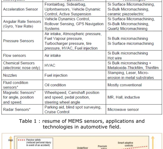
Table 1 : resume of MEMS sensors, applications and technologies in automotive field.
Figure 7: Evolution of passive and active safety features in cars [10].
1.5
Specifications for automotive electronics
The design of electronics for automotive applications must necessarily comply with the severe specifications of this field. A strict requirement of such devices concerns performances, first of all in terms of power consumption, area and cost. The high numbers of ECUs simultaneously working inside a car and the growing impact of electronics on the vehicle cost are pushing towards a reduction of available power for each electronic system, together with the need to combine multiple functionalities inside a smaller number of modules in order to optimize power
consumption and decrease the expensive demands of
interconnection resources. Regarding the edges of such complex units, i.e. the sensing elements, the related specifications may add further requirements with respect to the ECU functionality they belong to. While sensors working in the infotainment sphere share specifications with most of consumer electronics, those being part of active safety systems or body electronics have often stricter requirements in terms of noise, sensitivity and stability over temperature.
A maybe even bigger challenge for automotive electronics designers concerns the reliability issues. Car manufacturers are competing in a difficult and almost zero-growth market. Robustness is a powerful mean to attract customers and claim superior quality with respect to competitors. For this reason they tend to raise as much as possible the expectations on the operative life of the vehicle (the so called "mission profile"), resulting in always tighter specifications for the related electronics. BMW for example, assumes a car service life of 15 years, with 300000 Km distance and 6000 hours of operation, 12000 engine starts and environment temperature between -40°C and +85°C [11]. Moreover OEM customer quality level requirements increased from defects over 100 units produced to parts per million and are expected to raise to parts per billion in the near future in the quest for absolute zero defects.
Electronics, as a part of the vehicle, has to guarantee the compliance to such standards, with the added difficulty of operating in harsh environment. The electronics products in vehicles, especially under-hood components, work in severe conditions, including petroleum vapours, vibration (up to 10g rms near the engine), moisture, various fluids, dirt, chemicals and electro-magnetic interference. Besides all these, automotive
microelectronics must sustain temperatures well above the traditional maximum operating temperatures for consumer electronics, as in Table 2.
Electronics Operating Temperature
Consumer 0 °C to +70 °C
Industry -40 °C to +85 °C
Automotive -40 °C to +125 °C
Military -55 °C to +125 °C
Table 2: Thermal operating environments [12].
Protract exposure to high temperature can affect badly the behaviour of an integrated circuit. The main consequence of high operating temperature is a faster wearing of the device: as a matter of fact, during testing the average life expectancy of a component is calculated statistically from the faults detected in a set of samples working continuously at high T or subject to a number of temperature cycles. According to experimental laws [13], the medium junction temperature shortens the device life time exponentially. This implies that when the specified operating temperature gets too high (also considering the physical limits of working T for the silicon substrate, around 125 °C) it becomes critical (or too time consuming) to evaluate correctly the life expectancy of the electronic system. Such issues obviously conflict with the long term reliability required from the car manufacturers. Table 3 resumes the worst conditions to be faced by automotive electronic devices according to their position inside the vehicle.
Location Typical Continuous
Max Temperature Vibration Level Fluid Exposure On engine
On transmission 140°C Up to 10 g rms Harsh
At the engine
(intake manifold) 125°C Up to 10 g rms Harsh
Under hood
(near engine) 120°C 3 – 5 g rms Harsh
Undrer hood
(remote location) 105°C 3 – 5 g rms Harsh
Exterior 70°C 3 – 5 g rms Harsh
Passenger
compartment 70-80°C 3 – 5 g rms Benign
Table 3: Automotive temperature extremes (Delphi Delco Electronic Systems) [14].
1.6
Technologies and electronics design issues
Increasing time-to-market pressures and the availability of shrinking process technologies (as the Moore’s law is showing no sign of outdating) are the two fundamental forces driving designers, design methodologies, and EDA tools and flows today.
Figure 8: Moore’s law: projections and integration capability over the last 30 years [source: Intel Corporation].
On one hand, market pressures together with the added integration afforded by the latest technologies, have forced a move to higher levels of abstraction to cope with the added complexity in design. On the other hand, shrinking processes have also caused a move in the opposite direction: because of the increasing significance of physical effects, there has been a need to observe lower levels of detail. Signal integrity, electro-migration, and power analysis are adding severe complications to design methodologies already stressed by the increasing device count.
Figure 9: Design drivers and design methodology gaps [15]. These stresses uncover significant methodology gaps, which occur both between abstraction layers as well as within them. Design methodologies, tools, and flows, evolve to try to hold the design “system” together. Designers are driven to take advantage of the smaller process technologies, putting entire systems on chips: analog blocks, digital hardware, microcontrollers with memories and so on. In this way they succeed in reducing the product cost and fulfil the market demands, but also have to deal with a complexity difficult to be handled. In this scenario, top-down design methodologies have become a must [16]. In a basic top-down approach, the chip architecture is defined as a block diagram and simulated and optimized using either a Mixed Signal HDL simulator or a system simulator. From the high-level simulation, requirements for the individual circuit blocks are derived. Circuits are then designed individually to meet these specifications. Finally, the entire chip is laid out and verified against the original requirements.
Designers and EDA tools have to keep under control an increasing number (and various categories) of constraints when implementing mixed signal SoCs. Physical constraints apply to the physical entities used to implement the layout. Examples are distances, area and aspect ratio, alignment between instances. Electrical constraints apply to specific signals in the circuit. Examples are timing, parasitics, IR drop, crosstalk noise, substrate coupling noise and electro-migration. Design constraints are used to characterize the behavior of individual components in terms of their I/O signals and performance. Examples are throughput, slew rate, bandwidth, gain, phase margin, power dissipation, jitter, etc. With complex AMS chips, design constraints might include specifications on sophisticated measurements such as distortion, noise and frequency response.
Due to the high complexity of modern SoCs and the large design effort thus required, it is hoped that the mixed-signal blocks can
be designed in advance as relatively generic components and incorporated into many designs. To support this, the mixed-signal blocks must be designed for reuse: at a minimum this implies that should be available certain documentation that describes the block. Standards that specify what type of documentation is required have been set by the Virtual Socket Interface Alliance (VSIA) [17]. In addition, if the block is large it may be required to be embedded in special interface collars to make it easier to import them into an ASIC-SOC. Design for reuse is effective only in case that developing a module for future reuse and customizing it takes significantly less effort than redesigning the block for a new application. An important task when preparing a block for reuse is generating a high-level model of the block that captures its essential behavior in order to be able to evaluate the suitability of the block for use in follow-on projects.
For what concerns more specifically the technologies for automotive applications, Figure 10 explains the trend over the last ten years. While pure digital devices can follow the pace of consumer and industry electronics, affording the front-end CMOS processes, mixed signal SoCs often employ derivate technologies (such as HVCMOS or BCD), which fit better the implementation of high performance analog cells and also allow the integration of power devices.
Figure 10: Technologies in automotive ICs [source: Robert Bosch GmbH]
In terms of dimensioning the automotive technologies have the same shrinking trend as front-end CMOS, simply with a few years gap that the latest BCD processes are trying to reduce (for example 0.35 µm BCD6 comes almost 10 years after the corresponding CMOS size appearance). This gap originates from the need to provide sufficient analog characterization of the
featured devices, after the CMOS process modification for the integration of bipolar transistors and DMOS. Moreover, the strict requirements of automotive standards (as mentioned in paragraph 1.5) impose accurate process verification before release.
Bibliography
[1] ‘World Automotive Semiconductor Markets’,
http://www.electronics.ca/reports/ic/semiconductor_markets.html
[2] Navet, N.; Song, Y.; Simonot-Lion, F.; Wilwert, C.; “Trends in Automotive Communication Systems”, Proceedings of the IEEE Volume 93, Issue 6, June 2005 Page(s):1204 - 1223
[3] ‘World Markets for Mixed Signal SoC in Automobiles’ , www.marketresearch.com
[4] ‘Inertial MEMS sensors for consumer applications’ by Richard Dixon and
Jérémie Bouchaud, Wicht Technologie Consulting
http://www.memsinvestorjournal.com/2006/05/inertial_mems_s.html
[5] ‘World Automotive Sensors’,
http://www.electronics.ca/reports/instruments-sensors/automotive_sensors.html
[6] Vigna, B.; “Future of MEMS: An industry point of view”, Thermal, Mechanical and Multiphysics Simulation and Experiments in Micro-Electronics and Micro-Systems, 2006. EuroSime 2006. 7th International Conference on, 24-26 April 2006 Page(s):1 - 8
[7] ‘MEMS Applications Automotive’,
http://www.st.com/stonline/products/technologies/mems/applications/auto. htm
[8] ‘Automobile Safety’, Wikipedia
[9] AWAKE, System for Effective Assessment of Driver Vigilance and Warning According to Traffic Risk Estimation, http://www.awake-eu.org/ [10]G. Leen, D. Heffernan, “Expanding automotive electronic systems,”
Computer, Vol. 35, no. 1, January 2002, pp. 88-93.
[11]‘Targets and Requirements for Robust Automotive Electronics’, BMW group
[12]Ohadi, M.; Jianwei Qi; “Thermal Management of Harsh-Environment Electronics”, Semiconductor Thermal Measurement and Management Symposium, 2004. Twentieth Annual IEEE 9-11 Mar 2004 Page(s):231 - 240
[13]R. Amro; J. Lutz; A. Lindemann; “Power Cycling with High Temperature Swing of Discrete Components based on Different Technologies” Proc. Of 35th annual IEEE power electronics specialists conference, pp.2593-2598, Aachen, Germany,2004
[14]M. R. Fairchild, R. B. Snyder, C. W. Berlin, and D. H. R. Sarma, “Emerging substrate technologies for harsh-environment automotive electronics applications,”, SAE Technical Paper Series 2002-01-1052. [15]Ken Kundert, Henry Chang, Dan Jefferies, Gilles Lamant, Enrico Malavasi,
Fred Sendig, “Design of Mixed-Signal Systems on Chip”, IEEE Transactions on Computer-Aided Design of Integrated Circuits and Systems, vol. 19, no. 12, pp. 1561-1571, December 2000.
[16]H. Chang, E. Charbon, U. Choudhury, A. Demir, E. Felt, E. Liu, E. Malavasi, A. Sangiovanni-Vincentelli, I. Vassiliou, “A Top-Down, Constraint-Driven Design Methodology for Analog Integrated Circuits”, Kluwer Academic Publishers, 1997.
Chapter 2
D
ESIGN OF SENSOR INTERFACES
2.1
State of the art
The designer of electronic devices for automotive applications has to make his way in a fast growing but very competitive market. The key to success resides in the ability to handle the always increasing technology options (from MEMS advances to shrinking BCD processes), developing high performance products and fulfilling all the safety and reliability demands with short time-to-market. This leads to an inevitable trade-off between the need for the highest degree of optimization (in term of area, power and overall performances) and the market pressures for low cost and fast developed devices. While a full optimized ASIC requires noteworthy design efforts and often results in higher development costs (both time and money), a more generic and flexible chip can meet the market demands by addressing at once several similar applications and reduce its costs by having a longer production life. From these basic considerations comes the Universal Sensor Interface (USI) approach, a first answer to the issues concerning the design of sensor interfaces.
The USI implementation proposed in [18] integrates a number of high performance optimized analog front-ends, in order to address the different conditioning needs of the various sensor classes (for example capacitive, resistive or inductive sensors). Using a voltage-to-period converter, the signal coming from the analog front-end is digitalized and a microcontroller or DSP handles the data and performs further digital processing.
Figure 11: Block diagram of the USI [18].
This approach aims to reduce costs by merging and re-evaluating the functions of the sensors, actuators, analog interfacing circuits and digital processors in overall design [19]. In practice, under the assumption that a complex system needs to process at the same time the information of many different sensors, a lot of conditioning electronics can be shared between several functionalities and thus a global area and cost saving is achieved. Unfortunately, such system does not foresee any customization possibility for specific sensor needs, therefore resulting in good performances but not up to the strict requirements of demanding fields like the automotive one.
Figure 12: Example of complex sensor system architecture with USI [20].
A similar approach more specifically oriented towards MEMS and called Universal Micro-Sensor Interface (UMSI) [21] expands the capability of the USI circuits. It implements a network-capable sensor bus, integrates programmable readout circuits for multiple signal modes, and includes a standard interface for application-specific peripherals. Up to 255 UMSI chips can be connected in a complex sensor system and each UMSI can interface with up to 8 capacitive, resistive, and/or voltage output devices.
Such implementation eases the construction of a sensor network with numerous nodes (which is indeed a need in several applications, among which also the automotive stands), yet the featured basic and generic analog front-end does not fit the performance demands of modern automotive sensor interfaces.
Figure 13: UMSI chip and optional external components.
2.2
Platform Based Design
The technical difficulties exposed in Paragraph 1.6 have not been overcome by approaches like Universal Sensor Interface. In the last years, the progress of silicon technology has been followed by the definition and the increasing application of Platform Based Design [22], a methodology conceived to cope with the most significant issues of modern ASIC development:
1. Manufacturing cost depends mainly on the hardware components of the product. Minimizing the size of the chip implies tailoring the hardware architecture to the functionality of the product. However, the cost of a state-of-the-art fabrication facility continues to rise.
2. NRE (Non-Recurrent Engineering) costs associated with the design and toolings of complex chips are growing rapidly. The cost of masks will grow even more rapidly for the most shrunk geometries, adding even more to the up-front NRE for a new design. Furthermore, the cost of developing and implementing a comprehensive test for such complex designs will continue to represent an increasing fraction of a total design cost unless new approaches are developed.
3. Design costs are exponentially rising due to the increased complexity of the products, the challenges posed by physical effects for deep sub-micron and the limited human resources. Design productivity is falling behind exponentially with respect to the technology advances. Time-to-market constraints are also growing at such a fast pace that even if costs were not an issue, it is becoming plainly impossible to develop complex parts within the constraints. An additional problem is the lack of skilled work force that could implement future IC’s considering the system aspects of the design and all second order physical effects that will be of primary importance in deep sub micron.
A platform [23] represents a layer in the design flow for which the underlying, subsequent design flow steps are abstracted. Thus a design from conception to implementation can be seen as a set of platforms (abstraction layers) and of methods to transform the design from one platform to the next. Platform based design provides a rigorous foundation to design re-use, correct-by-construction assembly of pre-designed and pre-characterized components (versus full-custom design methods), design flexibility (through an extended use of reconfigurable and programmable modules) and efficient compilation from specifications to implementations. At the same time, it allows to trade-off various components of manufacturing, NRE and design costs while sacrificing as little as possible potential design performance.
In general, a platform is made of a library of components that can be assembled to generate a design at that level of abstraction. The library may contain both computational blocks and communication components and each element of the library has a characterization in terms of performance parameters and supported functionality.
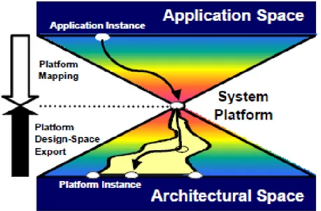
Figure 14: System platform layer and design flow. The system platform effectively decouples the application
development process (the upper triangle) from the architecture implementation process (the lower triangle). For every platform level, there is a set of methods used to map the upper layers of abstraction into the platform and a set of methods used to estimate performances of lower level abstractions.
A platform instance is a set of architecture components that are selected from the library and whose parameters are set, according to needs imposed by specifications.
Platforms should be defined to eliminate large loop designs iterations: they should restrict design space via new forms of regularity and structure that surrender some design potential for lower cost and first-pass success.
A critical step of the platform-based design process is the definition of intermediate platforms to support predictability, which enables the abstraction of implementation detail to facilitate higher-level optimization, and verifiability, i.e. the ability to formally ensure correctness.
2.3
Generic platform for inertial sensors
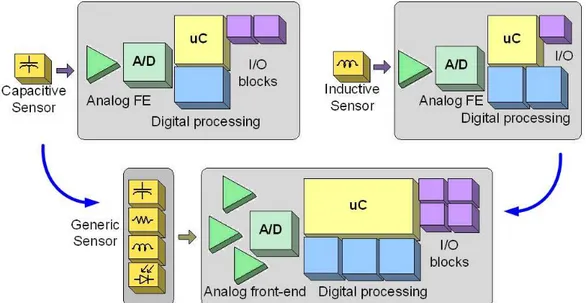
The theory of Platform Based Design expressed in previous paragraph has been employed in the development of a platform for inertial sensors conditioning in automotive applications. With respect to the USI approach, the aim is not to implement a single chip which can address a wide range of inertial sensors in MEMS technology (as it would result in a lower level of performances and an overhead of resources that the automotive field cannot afford),
but to keep the generality only at the system platform level (thus only as a design concept instead of a silicon implementation), while the highest level of optimization can be pursued in the platform implementations (each one dedicated to a target sensor). Figure 15 basically resumes the development of a Universal Interface: according to the blocks needed for conditioning each sensor class, they are integrated into the USI, which can save some hardware as few blocks can be shared by more than one sensor application. Of course some of them can’t be the optimal choice for specific conditioning purposes, and others won’t be used for certain application, therefore resulting in area and power overhead and increased parasites.
Figure 15: Building a Universal Sensor Interface
In the platform based approach instead [24], all the required blocks for different applications are collected inside the generic platform as a library of building blocks, which aim to be part of the signal processing path for inertial sensors. This platform represent the highest level of abstraction and thus its components are described as behavioural blocks in a proper language (for example MATLAB™), without any specification about their physical implementation (for instance whether they will be hardware or software, analog or digital). The platform itself doesn’t even contain any indication of the processing architecture, as this choice will be made at a further step considering the target application.
2.4
Design flow
prototyping System Level Description (MATLAB) MATLAB sim. VHDL Behavioral VHDL RTL VHDL Gate Level HDL sim. partitioning VHDL-AMS Schematic SPICE sim. Software ASIC FPGA AFE + sensorFigure 16: Design flow.
In the sensor conditioning field, the use of MATLAB™ language for the system platform eases the design space exploration phase and the subsequent tightening of each component specification before passing to the next platform at a lower abstraction level. In fact, the target sensor itself can be modelled and employed in simulations to evaluate the best conditioning architecture. In this way the computational blocks can be first generically modelled in their behaviour and then better defined through a set of specifications: for example, a basic multiplier block during the architecture evaluation can be provided step by step with more specification (for example output saturation limit, input dynamic range, etc…) in order to gather enough information for deciding
the best implementation for the block (analog or digital) and setting the final specifications (in the digital case for instance, the proper bit true model, clock frequency and data-paths width).
The aim of the MATLAB™ simulation at system level is to find a suitable conditioning architecture for the target sensor and perform a proper partitioning of the used blocks between analog cells, digital hardware and software routines. If the MATLAB™ evaluation has been comprehensive enough, the partitioning entails:
- the matching of in-detail-specified (but implementation independent) blocks with the nearest (for functionality and requirements) already available IP.
- the design from scratch of the remaining IPs (in the case none of those available fulfils the block requirements).
Except for the first run, a platform based design flow addresses a set of similar applications which are supposed to share several functionalities. For this reason, in this phase the reuse of existing IPs prevails on the development of new blocks and the more this design technique is exploited (i.e. the more applications are addressed), the less is needed to create new IPs.
In both cases anyway, at the HDL abstraction level, each block has to provide different views in order to guarantee the possibility to verify step by step the functionality of the block itself together with the overall system architecture. For example, digital hardware IPs need first of all a behavioural description (in VHDL) which resumes the block functionality hiding the details of the internal architecture and the possible implementation choices. The corresponding descriptions for the analog domain are VHDL-AMS models [25][26], which allow a first system level simulation (at the HDL abstraction level) that must match the results of the MATLAB™ investigation, thus validating the architectural and partitioning choices.
The use of VHDL-AMS has two main purposes. First, it summarizes the block specifications in a top-down approach before the design of the analog cell, constituting a reference for the analog designer and allowing a preliminary system validation during the development of the block (so the system level verification environment can be set up before the completion of each single block implementation). Once the schematic is ready, the same model can be updated with more detailed and realistic information coming from SPICE simulations, in a bottom-up data flow. The model can be then completed at the highest level of detail after layout, allowing the platform verification with even higher accuracy.
The main benefit of the VHDL-AMS approach is the possibility to check, at each stage of the design progress, the coherency of the whole system with respect to the initial behavioural model. In fact, though mixed signal HDL/SPICE simulation are supported by most tools, they result to be extremely slow (and may have convergence troubles) as the analog complexity raises over hundreds of transistors. VHDL-AMS instead, allows the extraction from the huge complexity of the schematic of only few parameters which depict the cell behaviour, in a way that the system simulation is dramatically speeded up but with no substantial loss of global accuracy [26].
Another important feature of the VHDL-AMS modelling is the possibility to detect bugs, shorts and system faults that can’t be seen by simply simulating cells or macro-blocks. A mixed-signal sensor interface parts itself almost equally between analog and digital sections. Each analog cell has tens of configuration switches, added to the routing configurability of input and test signals, which lead to a huge number of configuration strings, some of which may cause dangerous (or even killing) shorts or misbehaviours. Being as a matter of fact impossible to check all the possible configurations manually, VHDL-AMS allows the insertion of safety checks within each model (for example current or voltage over boundaries on a wire or node) that signal the potential bug during simulation, helping to implement a first time success silicon.
After the platform verification by means of VHDL/VHDL-AMS/C++ system simulations, the HDL abstraction level can be mapped to last developing stage before silicon, the prototype. In this phase, the needs of verification may depend strongly on the application and the implementation choices made at the higher levels. For instance, in case the design results to be mostly digital oriented (i.e. analog section much smaller than the digital one) the verification of the digital part assumes a predominant role and a suitable strategy can be the emulation of the analog functionality with a discrete-components front end, connected with a FPGA implementing all the ASIC digital blocks plus few add-ins for further test, evaluation and debug. This approach reduces development time and cost, but does not cover in a comprehensive way all the possible interactions between analog and digital domains. Moreover, it is not fit for half-digital-half-analog (or mostly analog) designs and the prototype can provide little information on final ASIC performances, because of the excessive level of parasites and disturbs in the discrete components setup with respect to the corresponding integrated analog front-end. In order to have a realistic and reliable prototype (for what concerns
performance estimation and feedback information for further improvements) the only possibility is to integrate the analog section into a test chip, at the cost of a substantial increase of design expenses and stretching of time-to-market. An effective solution to this drawback will be described in Chapter 3.
The prototyping phase concludes the design iteration with a bottom-up propagation of all the data collected by the prototype working with the target sensor, in order to update the HDL description and VHDL-AMS analog models and, in the end, the original MATLAB™ blocks, allowing a system evaluation with coherent results at each abstraction level. If the system specifications haven’t been met, improvements are to be evaluated and carried out at the top level and then propagated down to the physical implementation.
2.5
Case study: gyro sensor
In this paragraph a case study for the above mentioned platform based design flow is presented. The generic platform architecture has been customized for conditioning a gyroscopic angular rate sensor, and implemented in collaboration with Sensordynamics AG for a commercial chip.
i.
Gyro sensor
Vibrating ring gyroscopes consist of a circular ring provided with drive, sense and control electrodes [27]. Even though they are also available as discrete components, automotive applications push towards MEMS implementations [28], requiring stand-alone devices able to provide accurate yaw rate measurement.
Gyro sensors base their working on the Coriolis force acting on a vibrating mass: while the driving electrodes keep the ring vibrating along the primary direction (with fixed amplitude, around the z-axis in Figure 17 [28]), the rotation of the device (Ωx) causes
an energy transfer to the second vibrating mode, which is located at 90° from the primary mode (on the y-axis). The amplitude of this vibration is proportional to the angular rate, and in open loop mode it can be detected through a differential capacitance measure on the sense electrodes placed on the rectangular structure. A closed loop configuration exploits the control electrodes, by means of which the secondary vibration can be compensated, in order to let the sensor work around its rest point, thus achieving more linearity and accuracy.
Figure 17: Gyro sensor: Cross-section (a) and top view (b). The conditioning electronics for such sensors basically requires a Phase Locked Loop (PLL, for primary drive), which has to keep the ring in resonance (at a frequency of approximately 6 KHz), an Automatic Gain Control (AGC, to control the amplitude of this vibration) and a chain including demodulators, filters, temperature/offset compensation and modulators for secondary drive and rate sensing.
ii.
System architecture
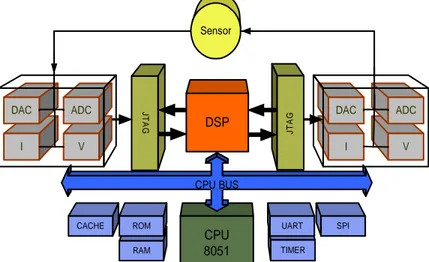
The generic platform architecture depicted in Figure 18 has been customized to the gyro sensor conditioning requirements, in order to achieve an almost optimal implementation for interfacing this kind of sensor, together with several communication resources for easier debugging, development and performance improvement. For what concerns the analog front end, it can be critical in automotive applications to meet the required noise, area and power consumption constraints within a wide temperature range (-40°C÷125°C). These limitations do not apply to the digital
counterpart: for this reason it’s preferable to use as little analog signal processing as possible and to perform most of the conditioning in the digital domain. Thus the analog section only absolves functions of driving sensor’s electrodes (through couples of DACs for each loop) and performing signal acquisition (by means of SAR ADCs, amplifiers and low pass filters). It also provides stable voltage and current references and clock to the digital section. CPU 8051 CACHE SPI J T A G CPU BUS V I DAC ADC V I DAC ADC RAM ROM TIMER UART Sensor J T A G DSP
Figure 18: Platform architecture
Each analog cell in the front-end is digitally controlled, and this programmability can be of paramount importance for the whole system functioning. Particular effort has been placed in building a reliable and efficient interface between the analog and digital world. A JTAG-like interface has been selected for the following reasons:
- The standard protocol has largely been studied and tested for several applications, so it guarantees high reliability since first implementation.
- JTAG bases on asynchronous communication, which limits clock skew issues that may lead to undetectable faults. - It employs a short number of wires (only 4 per chain),
thus resulting easy to route also on very complex chips. - It allows for full read-back capability (for fast verification
or debugging).
The digital section performs almost all the signal processing (within the DSP block), and manages the communication resources (through the CPU core). The DSP contains a chain of IPs for signal elaboration, featuring the blocks schematically depicted in Figure 19: its architecture and sub-blocks dimensioning are derived from the MATLAB™ model set up during the design space exploration phase.
Figure 19: DSP chain for gyro sensor conditioning.
Though all the required processing can be performed independently by analog front end and DSP block, a CPU core is also present to fulfil control, monitoring and communication tasks. These functionalities naturally find their best implementation via software routines, as they may vary through system updates and new system requirements.
SPI TIMER WDOG
UART 16-bit bus BRIDGE SFR bus 8051 CPU CACHE RAM ROM PC CACHE FPGA SPI EEPROM External SRAM SRAM ctrl
Figure 20: CPU core architecture with communication resources.
Control and monitoring are performed real-time by the processor on both DSP and analog front end: a routine constantly checks the system status by accessing the several readable registers spread along the processing chain (for example makes sure that the PLL is locked). Meanwhile other routines handle communication services,
Gyro
Analog FE JTAG like
PLL DEMOD DSP AGC DEMOD Temp, DC offset comp MOD primary drive primary pick-up secondary pick-up secondary drive RATE OUT
![Figure 2: Number of ECUs inside Volkswagen cars in the last 10 years [source: Volkswagen AG]](https://thumb-eu.123doks.com/thumbv2/123dokorg/7284551.85044/14.892.167.782.453.739/figure-number-ecus-inside-volkswagen-years-source-volkswagen.webp)
![Figure 3: Growth forecast for MEMS gyros and accelerometers up to year 2009 [4].](https://thumb-eu.123doks.com/thumbv2/123dokorg/7284551.85044/15.892.162.679.594.877/figure-growth-forecast-mems-gyros-accelerometers-year.webp)
![Figure 6: Value added electronics in cars. [source: BMW Group]](https://thumb-eu.123doks.com/thumbv2/123dokorg/7284551.85044/20.892.199.750.132.535/figure-value-added-electronics-cars-source-bmw-group.webp)
![Figure 8: Moore’s law: projections and integration capability over the last 30 years [source: Intel Corporation]](https://thumb-eu.123doks.com/thumbv2/123dokorg/7284551.85044/26.892.173.778.312.705/figure-moore-projections-integration-capability-source-intel-corporation.webp)
![Figure 9: Design drivers and design methodology gaps [15]. These stresses uncover significant methodology gaps, which occur both between abstraction layers as well as within them](https://thumb-eu.123doks.com/thumbv2/123dokorg/7284551.85044/27.892.132.710.132.345/figure-design-drivers-methodology-stresses-significant-methodology-abstraction.webp)
![Figure 10: Technologies in automotive ICs [source: Robert Bosch GmbH]](https://thumb-eu.123doks.com/thumbv2/123dokorg/7284551.85044/28.892.171.785.680.940/figure-technologies-automotive-ics-source-robert-bosch-gmbh.webp)