Performance and Reliability Comparison of 1T-1R
RRAM arrays with Amorphous and Polycrystalline
HfO
2
Alessandro Grossi
∗, Eduardo Perez
†, Cristian Zambelli
∗, Piero Olivo
∗, and Christian Wenger
†∗Universit`a degli Studi di Ferrara, Dip. di Ingegneria, ENDIF, Via G. Saragat 1, 44122 Ferrara, Italy
†IHP, Im Technologiepark 25, 15236 Frankfurt (Oder), Germany
E-mail: [email protected]
Abstract—In this work, a comparison between 1T-1R RRAM 4kbits arrays manufactured either with amorphous or polycrys-talline HfO2 in terms of performance, reliability, Set/Reset op-erations energy requirements, intra-cell and inter-cell variability during 10k Set/Reset cycles is reported. Polycrystalline array shows higher current ratio, lower switching voltages, lower power consumption, minor endurance degradation and higher overall yield than amorphous array. The drawbacks are represented by the higher Forming voltage, the larger read current distribution after Forming and the higher Reset voltage dispersion.
I. INTRODUCTION
Resistive Random Access Memories (RRAM) technology gathered significant interest for several applications [1]–[3]. RRAM behavior is based on the possibility of electrically modifying the conductance of a Metal-Insulator-Metal (MIM) stack: the Set operation moves the cell in a low resistive state (LRS), whereas Reset brings the cell in a high resistive state (HRS) [4], [5]. To activate such a switching behavior, some technologies require a preliminary Forming operation [6]–[8]. The choice of a proper MIM technology for RRAM cells, exhibiting good uniformity and low switching voltages, is therefore a key issue for array structures fabrication and reli-able electrical operation [9]. Such a process step is mandatory to bring this technology to a maturity level. In this work, a comparison between 1T-1R RRAM 4kbits arrays manu-factured either with amorphous [5] or polycrystalline [10]
HfO2is performed. In amorphous HfO2the conduction mainly
occurs through a conductive filament created during the Form-ing operation with highly variable concentration of defects,
whereas in polycristalline HfO2 the conduction occurs only
through grain boundaries with a very low defect concentration. These differences in terms of conduction properties and defect concentrations translate into different switching properties [9], with several implications on inter-cell (variations between cells) and intra-cell (cycle-to-cycle variations of any given cell) variability. In this work a comparison in terms of performance, reliability, Set/Reset operations energy requirements, intra-cell and inter-intra-cell variability during 10k endurance cycles is reported.
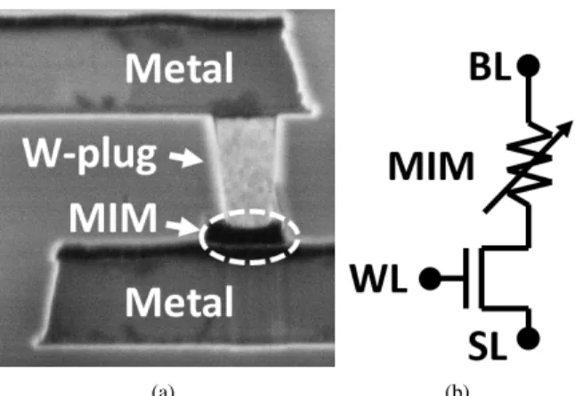
(a) (b)
Fig. 1. Cross-sectional STEM image (a) and schematic (b) of the 1T-1R cell integrated in the arrays.
II. EXPERIMENTALSETUP
The 1T-1R memory cells in the 4kbits arrays are constituted
by a select NMOS transistor manufactured with a 0.25 µm
BiCMOS technology whose drain is in series to the MIM stack. The wordline (WL) voltage applied to the gate of the NMOS transistor allows setting the cell current com-pliance. The cross-sectional Scanning Transmission Electron Microscopy (STEM) image of the cell and the 1T-1R cell schematic are reported in Fig. 1. The variable MIM resistor is composed by 150 nm TiN top and bottom electrode layers deposited by magnetron sputtering, a 7 nm Ti layer, and a 8
nm HfO2 layer deposited with two different Atomic Vapour
Deposition (AVD) processes resulting either in amorphous
(A) or polycrystalline (P) HfO2 films, respectively. The
re-sistor area is equal to 0.4 µm2. For amorphous films it has
been integrated also a resistor with larger area that shows
improved reliability and performance (i.e., 1 µm2) [4]. The
Forming/Set/Reset operations on the arrays were performed by using an Incremental Pulse and Verify algorithm [11]. The bitline (BL), sourceline (SL) and WL voltages applied during Forming, Set, Reset and Read operations are reported in Tab. I. Reset operations were performed by applying the WL voltage that allows maximizing the cells switching yield © 2016 IEEE. Personal use of this material is permitted. Permission from IEEE must be obtained for all other uses, in any current or future media, including reprinting/republishing this material for advertising or promotional purposes, creating new collective works, for resale or redistribution to servers or lists, or reuse of any
copyrighted component of this work in other works.
This is the accepted version of the paper. The published version can be found at ieeexplore.ieee.org/abstract/document/7440057/ The DOI of the published version is: 10.1109/ULIS.2016.7440057
TABLE I
FORMING, SET, RESET ANDREADVOLTAGEPARAMETERS. Operation VSL[V] VBL [V] VW L[V]
Forming 0 2-3.2 1.5
Set 0 0.2-3.2 1.5
Reset 0.2-3.2 0 2.5 (A)/ 2.8 (P)
Read 0 0.2 1.5
(2.8 V on array A and 2.5 V on array P) while avoiding
the breakdown of the HfO2 [12]. Pulses were applied during
Forming by increasing VBL with ∆VBL=0.01V, whereas
during Set and Reset ∆VBL=0.1V and ∆VSL=0.1V have been
used, respectively. Each pulse featured a duration of 10µs, with a rise/fall time of 1µs to avoid overshoot issues. Set operation was stopped on a cell when the read-verify current reached at least 20µA, whereas Reset was stopped when reached al least 10µA. Forming, Set and Reset BL/SL voltages necessary to reach the requested read-verify current targets are extracted
from the characterization data and labelled as VF ORM, VSET,
and VRES, respectively.
III. EXPERIMENTALRESULTS
1T-1R cell arrays integrated with A-HfO2 (A-array) with
small (0.4 µm2) and large (1 µm2) resistor area, and
P-HfO2 (P-array) resulted in a Forming Yield (calculated as
the cell percentage having a read verify current after
form-ing Iread ≥ 20µA) of 58%, 90%, and 95%, respectively.
Fig. 2 shows the average current ratios between Low Resistive State (LRS) and High Resistive State (HRS) read currents
(ILRS/IHRS), calculated on the entire cells population during
Set/Reset cycling, and their relative dispersion coefficient. The
dispersion coefficient, defined as (σ2/µ), has been used to
evaluate the cell-to-cell variability. The minimum current ratio that allows to correcly discriminate between HRS and LRS
(ILRS/IHRS >2) is indicated for comparison purposes [5].
Due to the faster cell degradation, the average ratios of
A-arrays with resistor area of 0.4 µm2 and 1 µm2 cross the
minimum ratio limit after 200 and 1k cycles, respectively. P-array showed higher ratio (≈ 2.8) even after 10k cycles, but also a higher dispersion coefficient after Forming (i.e., cycle 1). The grain boundaries conduction mechanism in the
polycrystalline HfO2 structure could be the reason of the
higher cell-to-cell variability in P-arrays [13]. A-array with
resistor area of 1 µm2 shows a slightly higher average ratio
and a slower degradation than A-array with resistor area of
0.4µm2. In smaller cells the presence of defects in the HfO
2
stack has a stronger impact on the performance since makes the switching operations more difficult to control, speeds up the degradation and increases the overall inter-cell variability [14].
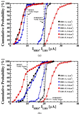
Fig. 3 shows a comparison between ILRS and IHRS
cu-mulative distributions measured at cycle 1 and after the 10k Set/Reset cycling test: A-arrays show more compact distribu-tions at cycle 1, however after cycling P-array shows a higher percentage of correctly switching cells reaching the Set/Reset
verify targets. IHRS cumulative distribution in P-array shows
100 101 102 103 104 Switching Cycles 0 0.5 1 1.5 2 2.5 3 3.5 4 ILRS /IHRS A (1µm2) A (0.4 µm2) P (0.4 µm2) Min. Ratio (a) 100 101 102 103 104 Switching Cycles 0 2 4 6 8 10 12 14 16 I LRS /I HRS Disp. Coeff. A (1 µm2) A (0.4 µm2) P (0.4 µm2) (b)
Fig. 2. ILRS/IH RScurrent ratio average values (a) and dispersion coefficients (b) calculated during cycling.
0 10 20 30 40 IHRS, ILRS [µA] 0 10 20 30 40 50 60 70 80 90 100 Cumulative Probability [%] HRS (A, 1µm2) LRS (A, 1µm2) HRS(A, 0.4µm2) LRS (A, 0.4µm2) HRS (P, 0.4µm2) LRS (P, 0.4µm2) RESET Verify Target FORM/SET Verify Target (a) 0 10 20 30 40 IHRS, ILRS [µA] 0 10 20 30 40 50 60 70 80 90 100 Cumulative Probability [%] HRS (A, 1µm2) LRS (A, 1µm2) HRS (A, 0.4µm2) LRS (A, 0.4µm2) HRS (P, 0.4µm2) LRS (P, 0.4µm2) RESET Verify Target FORM/SET Verify Target (b)
Fig. 3. IH RSand ILRScumulative distributions at cycle 1 (a) and at cycle 10k (b).
a larger distribution tail at cycle 1 compared to A-arrays. After 10k cycles the cells degradation makes more difficult to break or re-create the filament, hence the voltage requested to reach the verify target increases as well as the number of cells not able to reach the verify target. An enlargement of the upper tail in P-array HRS distribution can be observed whereas on A-arrays a strong shift of the distributions towards higher currents occurs, since a higher number of cells is not able reach the Reset threshold. The reason of the lower ratio in A-array with small resistor area can be explained by the cumulative
distributions, since they show lower ILRS and higher IHRS
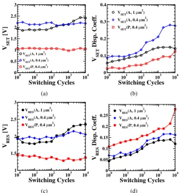
100 101 102 103 104 Switching Cycles 0 0.5 1 1.5 2 2.5 3 VSET [V] VSET(A, 1 µm 2 ) VSET(A, 0.4 µm 2 ) VSET(P, 0.4 µm 2 ) (a) 100 101 102 103 104 Switching Cycles 0 0.1 0.2 0.3 0.4 VSET Disp. Coeff. VSET(A, 1 µm2) VSET(A, 0.4 µm2) VSET(P, 0.4 µm2) (b) 100 101 102 103 104 Switching Cycles 1 1.5 2 2.5 3 VRES [V] VRES(A, 1 µm2) VRES(A, 0.4 µm2) VRES(P, 0.4 µm2) (c) 100 101 102 103 104 Switching Cycles 0 0.05 0.1 0.15 0.2 0.25 VRES Disp. Coeff. VRES(A, 1 µm2) VRES(A, 0.4 µm2) VRES(P, 0.4 µm2) (d)
Fig. 4. VSET and VRES average values (a,c) and dispersion coefficients (b,d) calculated during cycling.
10k cycles. In ILRScumulative distributions the cells not able
to reach the Set verify target generate a lower tail on P-arrays after 10k cycles, whereas on A-arrays a higher number of cells is not able to reach the Set verify target especially when
cells with resistor area of 0.4µm2are considered. This results
into a strong shift of the distributions towards lower currents, especially in A-array with small resistor area that shows a high number of cells not reaching the Set verify target even at cycle 1.
Fig. 4 shows the average Set and Reset switching voltages
(VSET, VRES) and their relative dispersion coefficients: lower
VSET and VRES are required on P-array which also shows
no variations during Set/Reset cycling, whereas VSET, VRES
increase on A-arrays during cycling. VRES on P-array shows
the highest variability: such operation is critical and very difficult to control in RRAM arrays since it strongly depends on how the filament is created: over Forming, as well as endurance degradation, can make the filament difficult to
disrupt, increasing the VRES variability [11]. A-arrays show
similar behavior of the average VSET and VRES (a lower
average VSET is observed on A-array with larger resistor
area only up to 500 cycles), while a higher VSET and VRES
dispersion can be observed in A-array with smaller resistor area.
Fig. 5 shows the cumulative distributions of switching voltages during Forming, while Fig. 6 shows the Set and Reset switching voltages cumulative distributions at cycle 1 and after the Set/Reset cycling. Forming, Set and Reset incremental pulse algorithms starting point and last attempt are indicated, corresponding to the first and the last voltage pulse available in the incremental pulse and verify procedure [11]. P-array
re-0.0 0.5 1.0 1.5 2.0 2.5 3.0 3.5 4.0 VFORM[V] 0 10 20 30 40 50 60 70 80 90 100 Cumulative Probability [%]
Forming Algorithm Start
Forming Algorithm Last Attempt A, 1µm2 A, 0.4µm2 P, 0.4µm2
Fig. 5. VF ORM cumulative distributions.
0.0 0.5 1.0 1.5 2.0 2.5 3.0 3.5 4.0 VSET, VRES [V] 0 10 20 30 40 50 60 70 80 90 100 Cumulative Probability [%] A, 0.4µm2 A, 1µm2 P, 0.4µm2 SET RES Set/Reset Algorithm Start Set/Reset Algorithm Last Attempt (a) 0.0 0.5 1.0 1.5 2.0 2.5 3.0 3.5 4.0 VSET, VRES [V] 0 10 20 30 40 50 60 70 80 90 100 Cumulative Probability [%] A, 0.4µm2 A, 1µm2 P, 0.4µm2 SET RES Set/Reset
Algorithm Start Set/ResetAlgorithm Last Attempt
(b)
Fig. 6. VSETand VREScumulative distributions at cycle 1 (a) and at cycle 10k (b).
quires lower VSET and VRESbut higher VF ORM if compared
to A-array with the same resistor area. A-array with larger
resistor area requires higher VF ORM. Moreover, it can be
observed that ≈ 40% of the devices with smaller resistor area
reached the forming threshold at VF ORM=2 V, corresponding
to the first attempt of the Forming Algorithm. Since P-array
shows a more compact distribution on VSET and a larger
VRES than A-arrays, faster Set operation could be reliably
used on P-array, whereas on Reset an incremental pulse with verify technique is required to ensure good reliability. A-arrays
show large distributions on both VSET and VRES, hence
the adaptation of incremental pulse with verify techniques is mandatory on such arrays.
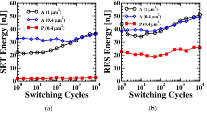
100 101 102 103 104 Switching Cycles 0 10 20 30 40 50 60 SET Energy [nJ] A (1 µm2) A (0.4 µm2) P (0.4 µm2) (a) 100 101 102 103 104 Switching Cycles 0 10 20 30 40 50 60 RES Energy [nJ] A (1 µm2) A (0.4 µm2) P (0.4 µm2) (b)
Fig. 7. Energy required to perform Set (a) and Reset (b) operations as a function of the Set/Reset cycle number.
Fig. 7 shows the average energy required to perform Set and Reset operations on a single cell. The overall energy required to create/disrupt the conductive filament during Set/Reset operations has been calculated as [11]:
E =
n
X
i=1
Vpulse,i∗Ipulse,i∗Tpulse+ Vread∗Iread,i∗Tread (1)
Where n is the number of reset pulses applied during
incremental pulse operation, Vpulse,i is the pulse voltage
applied at stepi, Ipulse,iis the current flowing through RRAM
cell during pulse i application, Tpulse = 10µs is the pulse
length,Vread =0.2 V is the read voltage applied during verify
operation,Iread,iis the current read on the RRAM during read
verify stepi, and Tread= 10µs is the verify pulse length.
P-array shows lower power consumption with a lower increase
during cycling thanks to a lower VSET and VRES. A-arrays
with different resistor area show similar power consumption during Reset operation, whereas a lower consumption during Set is observed on A-array with larger resistor area only up to 500 cycles since cells with larger resistor area require lower
VSET.
IV. CONCLUSIONS
1T-1R RRAM arrays manufactured with P-HfO2 shows
several advantages compared to A-HfO2even considering their
improved process: higher current ratio, lower switching volt-ages, lower power consumption, minor endurance degradation and higher overall yield. Moreover, P-array show very low
VSET variability, hence faster Set operation could be reliably
performed. P-array disadvantages are represented by the larger HRS distribution after Forming, the higher Reset voltage
dispersion and the higher VF ORM if compared to A-array
with the same resistor area, however but it must be pointed out that Forming operation is performed only once. The grain boundaries conduction mechanism in the polycrystalline
HfO2 structure could be the reason of the higher cell-to-cell
variability in P-arrays.
ACKNOWLEDGMENTS
This work was supported by the European Union’s H2020
research and innovation programme under grant agreement No
640073.
REFERENCES
[1] S. Tanachutiwat, M. Liu, and W. Wang, “FPGA Based on Integration of CMOS and RRAM,” IEEE Trans. on Very Large Scale Integration
(VLSI) Systems, vol. 19, no. 11, pp. 2023–2032, Nov 2011.
[2] D. Garbin, E. Vianello, O. Bichler, Q. Rafhay, C. Gamrat, G. Ghibaudo, B. DeSalvo, and L. Perniola, “HfO2-Based OxRAM Devices as Synapses for Convolutional Neural Networks,” IEEE Trans. on Electron
Devices, vol. 62, no. 8, pp. 2494–2501, Aug 2015.
[3] T. Xu and V. Leppanen, “Analysing emerging memory technologies for big data and signal processing applications,” in Digital Information
Processing and Communications (ICDIPC), 2015 Fifth International Conference on, Oct 2015, pp. 104–109.
[4] C. Zambelli, A. Grossi, D. Walczyk, T. Bertaud, B. Tillack, T. Schroeder, V. Stikanov, P. Olivo, and C. Walczyk, “Statistical analysis of resistive switching characteristics in ReRAM test arrays,” in IEEE Int. Conf. on
Microelectronics Test Structures (ICMTS), Mar 2014, pp. 27–31. [5] C. Zambelli, A. Grossi, P. Olivo, D. Walczyk, J. Dabrowski, B. Tillack,
T. Schroeder, R. Kraemer, V. Stikanov, and C. Walczyk, “Electrical characterization of read window in ReRAM arrays under different SET/RESET cycling conditions,” in IEEE Int. Memory Workshop (IMW), May 2014, pp. 1–4.
[6] D. Walczyk, T. Bertaud, M. Sowinska, M. Lukosius, M. A. Schubert, A. Fox, D. Wolansky, A. Scheit, M. Fraschke, G. Schoof, C. Wolf, R. Kraemer, B. Tillack, R. Korolevych, V. Stikanov, C. Wenger, T. Schroeder, and C. Walczyk, “Resistive switching behavior in TiN/HfO2/Ti/TiN devices,” in Int. Semiconductor Conf.
Dresden-Grenoble (ISCDG), Sept 2012, pp. 143–146.
[7] P. Lorenzi, R. Rao, and F. Irrera, “Forming kinetics in HfO2-based RRAM cells,” IEEE Trans. on Electron Devices, vol. 60, no. 1, pp. 438–443, 2013.
[8] A. Grossi, D. Walczyk, C. Zambelli, E. Miranda, P. Olivo, V. Stikanov, A. Feriani, J. Sune, G. Schoof, R. Kraemer, B. Tillack, A. Fox, T. Schroeder, C. Wenger, and C. Walczyk, “Impact of Intercell and Intracell Variability on Forming and Switching Parameters in RRAM Arrays,” IEEE Trans. on Electron Devices, vol. 62, no. 8, pp. 2502– 2509, Aug 2015.
[9] K. Morgan, R. Huang, S. Pearce, and C. de Groot, “The effect of atomic layer deposition temperature on switching properties of HfOx resistive RAM devices,” in IEEE Int. Symp. on Circuits and Systems (ISCAS), June 2014, pp. 432–435.
[10] H.-D. Kim, F. Crupi, M. Lukosius, A. Trusch, C. Walczyk, and C. Wenger, “Resistive switching characteristics of integrated polycrys-talline hafnium oxide based one transistor and one resistor devices fabricated by atomic vapor deposition methods,” Journal of Vacuum
Science and Technology B, vol. 33, no. 5, pp. 052 204.1–052 204.5, 2015. [11] A. Grossi, C. Zambelli, P. Olivo, E. Miranda, V. Stikanov, C. Walczyk, and C. Wenger, “Electrical characterization and modeling of pulse-based forming techniques in RRAM arrays,” Solid-State
Electronics, vol. 115, Part A, pp. 17 – 25, 2016. [Online]. Available: http://www.sciencedirect.com/science/article/pii/S0038110115002828 [12] A. Grossi, C. Zambelli, P. Olivo, E. Miranda, V. Stikanov, T. Schroeder,
C. Walczyk, and C. Wenger, “Relationship among current fluctuations during forming, cell-to-cell variability and reliability in RRAM arrays,” in IEEE Int. Memory Workshop (IMW), May 2015, pp. 1–4.
[13] V. Iglesias, M. Porti, M. Nafra, X. Aymerich, P. Dudek, and G. Bersuker, “Dielectric breakdown in polycrystalline hafnium oxide gate dielectrics investigated by conductive atomic force microscopy,” Journal of Vacuum
Science and Technology B, vol. 29, no. 1, 2011.
[14] S. Balatti, S. Ambrogio, A. Cubeta, A. Calderoni, N. Ramaswamy, and D. Ielmini, “Voltage-dependent random telegraph noise (RTN) in HfOx resistive RAM,” in IEEE Int. Reliability Physics Symposium, June 2014, pp. MY.4.1–MY.4.6.