1/29
A Review on Efficient Self-Heating in Nanowire Sensors:
Prospects for Very-Low Power Devices
C. Fàbrega1,2, O. Casals1,2, F. Hernández-Ramírez1,2, J. D. Prades1,2,*
1 MIND, Department of Electronic & Biomedical Engineering, Universitat de Barcelona 2 Institute of Nanoscience and Nanotechnology (IN2UB), Universitat de Barcelona
C/ Martí i Franquès 1, E-08028 Barcelona, Spain *Corresponding author e-mail: [email protected]
Abstract:
Self-heating operation, or the use of the resistance-probing signal to warm up and control the temperature of nanowire devices, has been the subject of research for more than a decade. In this review, we summarize the most relevant achievements reported to date in the specialized literature. The state-of-the-art shows that this approach is serving to lower the power demand in temperature-activated devices, especially in conductometric gas sensors, but the simplicity of eliminating the heating element comes with the complexity of integrating 1-dimensional nanomaterials in electronic devices. Results show however that this is feasible, and in some cases, even cost-effective.
To contribute to the further development and optimization of the self-heating approach, we compile here a set of recommendations on how to increase the efficiency of the future devices. These suggestions aim at clarifying the impact on the power efficiency of factors like the nanowire cross-section, the electrical and thermal conductivities of the material, the thermal insulation characteristics, and the operating conditions.
To facilitate the comparison of the performances obtained in past and future works, we also propose a figure of merit: the efficient self-heating coefficient (ESH), which accounts for the maximum temperature increase (in Kelvin) per microwatt of Joule power dissipated in the material. In this way, ESH values about 1 or above are indicative of highly efficient technologies, capable of raising the temperature over hundreds of degrees with less than a milliwatt of dissipated power.
2/29
I
NDEX:
1 Introduction ... 3
1.1 Conductometric Gas Sensors ... 3
1.1.1 Power Consumption of Conductometric Gas Sensors ... 4
1.1.2 Nanomaterials for Conductometric Gas Sensors ... 5
1.2 Self-Heating in 1D Nanomaterials ... 5
2 State-of-the-Art in Self-Heating ... 8
2.1 Efficient Self-Heating ... 8
2.2 Control of the Self-Heating Effect ... 8
2.3 Calibration of the Self-Heating Effect ... 9
2.4 Towards Self-Heated Sensor Devices ... 10
2.5 Advantages ... 10
2.5.1 Low Power Consumption ... 10
2.5.2 Fast Thermal Response Times ... 11
2.5.3 Other Applications ... 12
2.6 Limitations: The Challenge of Integration ... 12
3 Designing Efficient Self-Heating: How-To? ... 13
3.1 Materials shape and dimensions ... 14
3.2 Electrical transport properties ... 15
3.3 Heat transport properties ... 16
3.4 Thermal loses with the substrate ... 17
3.5 Multiple Nanowires ... 18
3.6 Accurate Temperature Control ... 19
3.7 Recommendations for an Efficient Self-Heating ... 21
4 Conclusion ... 21
5 Acknowledgement ... 21
3/29
1 I
NTRODUCTIONControlling the operating conditions of a sensor is crucial to obtain accurate, repeatable, and long-term stable readings. Otherwise, factors like vibration, ambient light, or temperature can interfere with the sensor signal, leading to readings not related to the magnitude being monitored. To prevent this cross-talk interference, many sensor technologies integrate some kind of actuator, either mechanical, optical or thermal. This is, in most of the cases, the main power hungry part of the device [1].
Concerning temperature control, it is mostly based on electrical resistors (for heating) and thermoelectric elements (for heating and cooling). The optimization of their power budget has usually relayed on more miniaturization (to reduce the thermal masses to be heated up [2,3]), and on better thermal isolation (to minimize the thermal losses related to heat conduction through solid parts [4–6]). This trend already started in the first generation of sensors with active areas at a millimeter scale [7], which was later reduced to tens-to-hundreds of microns with the use of microfabrication techniques (MEMS) [3,5,8–11]. Today, with the advent of nanotechnology (NEMS), we are approaching to the sub-micron regime [12,13]. In fact, nanotechnology enables the use of a nanowire-based heating method with potential for ultra-low power consumption, the self-heating effect, which is the subject reviewed in the following pages.
1.1 C
ONDUCTOMETRICG
ASS
ENSORSChemical sensing is one of the fields in which the control of temperature is more critical. When there is an interaction between molecules in a fluid phase and a transducing substance (e.g. a liquid or a solid electrolyte [14,15], a semiconductor [16,17], a polymer [18–20], a catalyst [21,22], etc.), the temperature is usually a key parameter. In fact, the ambient temperature at which theses sensors operate has a strong influence on the sensing performance. To minimize this interference, sensors are normally operated at temperatures above the expected operational environment (e.g. above room temperature for environmental sensing, much higher temperatures for combustion monitoring in engines, boilers, etc.). This solution is more effective and simple than attempting to compensate temperature fluctuations by continuously cooling and heating the sensor.
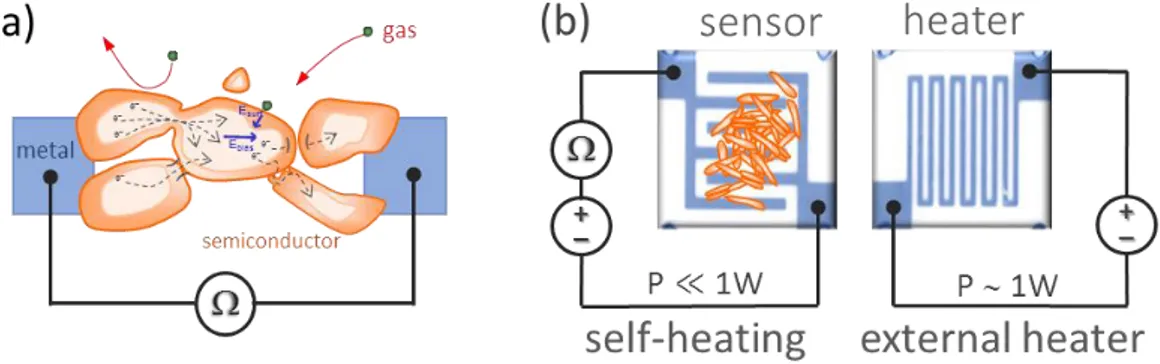
Conductometric gas sensors based on semiconductor materials are a paradigmatic example of the need for temperature control and the challenges related to achieving it in a power efficient manner [23]. In this type of sensors, the presence of gases is detected by monitoring the electrical resistance of a gas-sensitive material (typically a metal oxide [16,24], a polymer [18–20], a carbon-based material [25,26], or other semiconductors [27,28]) (see Figure 1.a). In the presence of gases, the resistance changes due to the chemical-electrical interactions between the gas molecules and the semiconductor surface, being most of these processes thermally activated [29].
The most accepted models describe this phenomenon as a steady balance between chemisorbed species at the surface, followed by their immediate desorption [30–32]. This dynamic picture is crucial to explain the recovery of the sensor baseline when the target gas is removed. From an energy point of view, the gas-solid interactions are ruled by a Lennard-Jones type of potential [33]. First, molecules may need some energy to approach the semiconductor surface to be adsorbed onto or to initiate a dissociative process. Later, some more energy might be needed to desorb the molecules back again into the gas phase. These steps define two energetic barriers for adsorption and desorption, which can normally be overcome by thermal means. That is the reason why, in most cases, the sensor response
4/29 displays a bell-shaped behavior versus the operating temperature, with a maximum corresponding to the optimal operating temperature at which adsorption and desorption are finely balanced [30,31]. Such temperatures are typically in the range of a few hundreds of degrees Celsius.
Figure 1: (a) A conductometric gas sensor based on a semiconductor material. Gas molecules interact with the semiconductor surface (Esurf), influencing the electron transport properties within the material. To measure these effects, an external bias signal (Ebias) is applied to the semiconductor placed across a pair of conducting electrodes. Ultimately, gas interactions are recorded as changes in the resistance/conductance of the device. (b) Physical construction of a conventional conductometric gas sensor: a two-sided substrate containing the sensor element (a semiconductor material and a pair of interdigitated metal electrodes) and the heating element (a metal meander). Both elements must be biased: the former to probe the resistance of the material, the latter to heat up the device. The amounts of power in each element are very dissimilar. In self-heating operation, the small amount of power used to probe the sensor resistance is enough to reach the optimum temperature for working, saving the need of a power-hungry heater.
1.1.1 Power Consumption of Conductometric Gas Sensors
The reduction of the optimal operating temperature in conductometric gas sensors has deserved much attention in the last decades, since the heating demand is the main source of power consumption of current technologies [23]. In fact, these high temperatures hamper the use of these sensors in temperature sensitive applications, such as explosive environment monitoring [34].
Research efforts demonstrate that operation temperature strongly depends on the physical and chemical properties of the semiconductor used and on the target gas. Therefore, studies have focused on new material combinations, such as the use of catalysts that could trigger the surface chemical reactions at lower temperatures [35–38]. In parallel, reducing the power consumption of the heating elements has also been a major topic of interest, and followed the same strategies used in other fields: reducing the thermal masses and minimizing the thermal losses [3,5,8–11].
Mature technologies, which have been commercially successful and available in the market for more than 20 years, require power figures in the range of a fraction of a watt (e.g. TGS68XX family from Figaro among many others). This is clearly too much for continuous operation in battery-operated systems or in sensor networks with strong constraints in the power budget.
The most advanced proposals based on MEMS (e.g. BME680 from Bosch Sensortec, TGS8100 from Figaro, AS-MLV-P2 from AMS, among others), offer figures in the order of tens of milliwatts, similar to the values reported for MEMS in the scientific literature [5,10,11]. Despite being a remarkable jump ahead, these values might be still excessive for power limited systems, if continued operation is required.
5/29 There are also reports proposing alternative methods for conductometric-like sensing operation that feature zero power consumption [39–42]. These systems are mostly based on integrating a source of energy collection/harvesting with the sensing element in a way that no further energy is needed to activate the gas-sensor interactions, providing even an energy surplus that can be used to read the sensor signal.
Anyhow, to build up a real sensor system, other components in demand of power must be considered. Typically, at least processing and communication units are always needed [43]. Even in the most austere configurations (e.g. with aggressive duty cycling), these components demand at least a few tens of microwatt [44]. Therefore, from a full-system perspective, this is a practicable true power threshold below which a sensor is regarded as an ultra-low, or an effectively-zero power component.
1.1.2 Nanomaterials for Conductometric Gas Sensors
It is well known that nanomaterials offer remarkable advantages in surface sensitive applications due to their large surface-to-volume ratio. Over the last 15 years, a number of reports demonstrated that reducing the size of the sensing materials is a systematic path towards larger responses and sensitivities [38,45–48]. These investigations also concluded that the shape of the materials plays an important role [49]. Specifically, sphere-type nanoparticles offer the largest surface-to-volume ratio, and therefore the larger sensor responses. In contrast, 1D-type nanoparticles (i.e. nanowires, nanorods, nanotubes, nanobelts, nanoribbons) offer also a convenient shape for integration in devices, since they already resemble a conduction channel or a 1D-path. It has also been argued that they exhibit better crystalline quality at the surface and bulk, which results into a better signal quality (e.g. higher stability, lower drift, more reversibility, faster response, etc.) [46].
These are the reasons why 1D nanomaterials have thoroughly been investigated for electrical sensing, concluding that they offer advantages in terms of signal quality provided that they are integrated into cost-effective devices [50,51]. Despite their functional advantages, this final integration step has hampered the widespread use in electronic devices to date.
1.2 S
ELF-H
EATING IN1D
N
ANOMATERIALSResearch with 1D nanoparticles has revealed an additional and unforeseen advantage when electrically driven. They can reach relatively high temperatures going through electrical tests (e.g. electrical resistance measurements), even with the small amounts of electrical power dissipated during the electrical probing [52,53] (Figure 2.b). This so-called self-heating effect makes it possible to reduce the power consumption of nanoscale devices down to the microwatt regime. In the case of conductometric gas sensors, this is a factor 1,000 lower than state-of-the-art microsensors mentioned above [54].
From a fundamental point of view, the self-heating effect is just the consequence of the Joule dissipation of power at a very small scale. Simple figures about the power dissipated per unit volume (i.e. the power density) can help to realize the dramatic differences when the device scale is reduced. As a matter of fact, one nanowire in self-heating operation can easily reach power densities 10,000 times larger than a conventional domestic heater (assuming 1 μW in a (100 nm)2 x 10 μm nanowire and 1 kW in a (1 mm)2 x 1 m heater filament).
The reason why self-heating is so efficient relays on the large power densities directly dissipated in the material that needs to be heated (e.g. a gas-sensitive nanowire). This is a
6/29 huge difference with conventional device architectures based on an independent heating element that warms up the sensor material (see Figure 1.b). Also, the heater needs to be electrically insulated from the sensor material, which adds even more material to heat. Therefore, the promise of the self-heating approach is double: (1) removing the need for an external heating element, and (2) reduction of the power consumption by eliminating the power consumption associated with this external heater.
A decade of research on self-heated devices has shown that this is a quite general phenomenon in nanowire-like structures with huge potential for efficient heating in miniaturized devices, which could be of application in several fields of sensing and actuation. This is illustrated in Table 1, which summarizes some of the works reporting self-heating effects in electronic devices. In the following section, we review this literature survey and present a detailed discussion about the advantages, requirements, and limitations of the self-heating approach.
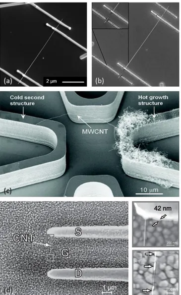
Figure 2: (a) A single SnO2 nanowire contacted with electron-beam assisted platinum deposition in a four-probe configuration before and (b) after a few hours of operation under electrical bias showing that the platinum contacts and the nanowire itself (inset) were destroyed by the high temperatures reached. (a & b) Reprinted figures with permission from Ref. [52]. Copyright 2007 by the American Physical Society. (c) The first single-wire type sensor displaying thermal effects in self-heating operation: a MWCNT detecting gas pressure changes due to changes in heat transfer with ambience. Adapted with permission from Ref. [55]. Copyright 2007 American Chemical Society. (d) General view and two detailed regions of an in situ grown SWCNT in a suspended configuration, which lead to record low power figures due to the good thermal insulation of the nanostructure. Reprinted from Ref. [12], with the permission of AIP Publishing.
7/29
Type Configuration Material Application Styp Rtyp
(Ω) T(K) max Vbias (V) I bias (A) P bias (W) ESH (K/W) τresp (s) Ref Year
@Tmax Tmax @Tmax @Tmax
Thin film Sputtered film SnO2 Gas sensor (CO) 1 mm x ? nm 1.3·10-3 150 50 3.9·10-2 1.9·106 9·10-5 - [56] 2003
Single wire Direct growth, bridging MWCNT Pressure-gas sensor (N2/Ar) 50 nm x 50 nm 1.0·105 - 1 1.0·10-5 10 - - [55] 2007
Single wire SnO2 Gas sensor (H2) 300 nm x 50 nm 2.0·106 200 10 5.0·10-6 50 4 - [57] 2008
Single wire SnO2 Gas sensor (NO2, CO, RH) 45 nm x 45 nm 3.0·108 300 90 3.0·10-7 27 10 10000 [54,58–60] 2008-10
Single wire Thin film + lithography Pd Gas sensor (H2) 65 nm x 65 nm 7.0·103 100 0.8 1.8·10-4 140 0.8 - [61] 2009
Single wire Thin film + lithography Pd Gas sensor (H2) 75 nm x 27 nm 8.8·104 128 19 2.2·10-4 4000 0.03 - [62] 2010
Single wire Nanoribbon Graphene Electron device 86 nm x 2nm 1.2·1015 10 3 2.6·10-5 78 0.1 - [63] 2011
Single wire Thin film + lithography Si -nc Thermoelectric device 200 nm x ? nm 2.0·104 1390 300 1.5·10-2 4.5·106 3·10-4 1 [64] 2011
Networked wires W18O49 - Pt Gas sensor (H2) 50 nm x 50 nm 7.0·102 25 6 8.6·10-3 5.1·104 5·10-4 - [65] 2011
Nanowire array Vertical nanowires InAs Gas sensor (NO2, NO) 75 nm x 75 nm 1.0·103 - 3.4 3.4·10-3 1.2·104 - - [66] 2012
Cross bar Thin film + etching C60 Electron device 200 nm x 200 m 9.6 183 3 3.1·10-1 9.4·105 2·10-4 - [67] 2012
Single wire Thin film + lithography Si - nc Thermoelectric device 130 nm x 1430 nm 2.5·103 1390 20 8.0·10-3 1.6·105 0.009 - [68] 2012
Single wire Suspended wire CNT Gas sensor (NO2) - 6.2·105 100 1.3 2.1·10-6 2.9 30 - [12] 2013
Single wire Thin film + lithography Si/Pd Gas sensor (H2) 100 nm x 50 nm - 60 18 - - - 0.1 [69] 2013
Single wire Vertical nanowires CNT Field emission 80 nm x 160 nm 1.6·106 1400 800 5.0·10-4 4.0·105 0.004 - [70] 2013
Single wire SnO2 Gas sensor (NO2) 60 nm x 60 nm 1.8·107 125 25 1.4·10-6 35 4 - [71] 2014
Multiple wires SnO2 Gas sensor (NO2) < 200 nm x 200 nm 1.8·107 - 40 2.3·10-6 90 - - [71] 2014
Networked wires SnO2 Gas sensor (NO2) < 200 nm x 200 nm 2.9·107 - 40 1.4·10-6 56 - - [71] 2014
Single wire Transistor InGaAs MOSFET 40 nm x 30 nm 2.7·103 15 4 1.5·10-3 6000 0.002 0.3 [72] 2015
Single wire Si - Pd Gas sensor (H2, CO, RH) 40 nm x 110 nm 4.6·104 35 1 2.2·10-5 160 0.2 - [73] 2015
Single wire Thin film + lithography In2O3 Gas sensor (NO2) 350 nm x 150 nm 6.5·103 140 5 9.0·10-4 4500 0.003 - [74] 2015
Multiple wires SnO2 Gas sensor (CO) 30 nm x 30 nm 4.9·1011 125 3730 7.5·10-9 28 5 17000 [75] 2015
Single strip Patterned, bridging Graphene Gas sensor (NO2, …) 3 graph. lay. x 5 μm 1.0·105 51 60 6.0·10-4 3.6·104 0.001 - [76] 2015
Single strip Patterned, bridging Graphene Visible light emitter 1 gr. lay. x <40 μm 1.5·104 2500 2.3 1.5·10-4 340 7 - [13] 2015
Networked wires Drop casting CNF Gas sensor (NO2, NH3, RH) 40 nm x 120 nm 1.0·104 270 20 2.0·10-3 4.0·104 0.008 <1000 [77–80] 2015-16
Multiple wires SnO2 Gas sensor (H2, NH3, H2S, …) 95 nm x 95 nm 1.0·104 275 18.4 1.9·10-3 3.5·104 0.01 - [81] 2017
Table 1: Summary of publications reporting quantitative information about self-heated devices based on nanomaterials. Styp and Rtyp, stand for the typical cross-section of the conduction path and its typical resistance, Tmax is the maximum increase of temperature reported in the paper (with respect to a reference temperature, usually 25ºC). Vbias, Ibias and Pbias are the electrical bias point at which this maximum temperature increase was achieved. ESH is the figure of merit Efficient Self-Heating coefficient, calculated at the maximum temperature reported. resp is the typical thermal response time of the materials submitted to a self-heating pulse. Plain faced figures correspond to number reported in the cited papers. Bold italic figures are values deduced in this work by simple calculations.
8/29
2 S
TATE-
OF-
THE-A
RT INS
ELF-H
EATING2.1 E
FFICIENTS
ELF-H
EATINGSince 1847, it is well-known that the electrical power dissipated in a resistive component leads to a temperature increase of the same [82]. The self-heating effect is nothing else than this effect, brought to such small scale that the temperature increase is remarkable, even when only small amounts of electrical power are applied. Therefore, it is only meaningful to talk about the self-heating effect in nanodevices, when it is efficient in terms of the amount of power needed for it to happen.
To make this discussion in quantitative terms, we propose here the definition of the following figure of merit: the Efficient Self-Heating coefficient (ESH),
𝐸𝑆𝐻 ∶= Δ𝑇
𝑃 (1)
where T is the temperature increase experimented by the device when it is subject to electrical power dissipation P. As said before, the advantages of the self-heating effect become relevant when power consumptions in the range of microwatts are achieved. Therefore, it is convenient to express the ESH coefficient in K/W units.
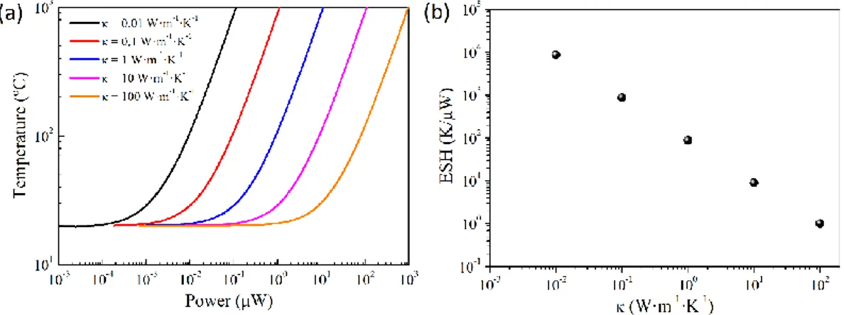
The literature works reviewed in Table 1 show that different materials and device configurations lead to a broad range of ESH values. It seems reasonable to state that the advantages of using the self-heating effect are evident when ESH figures larger than 1 are achieved (ESH > 1). This means an increase of a several Kelvin per microwatt consumed. In other words: if hundreds of Kelvin were needed, power consumptions well below the milliwatt regime were still attainable. As a reference, state-of-the-art microheaters (T 500C and P 10mW [5]) lead to ESH 0.05.
Finally, a word of caution regarding the interpretation of the ESH coefficients is needed. Our ability to measure the temperature with sub-micron spatial resolution in operando conditions is honestly limited (a full section is devoted to this issue below). With today’s technology, the ESH figures might only be relied on their order of magnitude. Therefore, the ESH values summarized in Table 1 should mostly be regarded as a rough guide to compare the overall performances achieved with alternative approaches.
2.2 C
ONTROL OF THES
ELF-H
EATINGE
FFECTIt is evident that the self-heating effect in nanowire-based devices can damage or destroy them, similarly to well-known equivalent effects in other microelectronic components [83,84] (Figure 2.a & .b). That is the reason why the effect was first described and regarded as a threat or as an experimental challenge to prevent in nanowire devices [52]. In fact, suppliers of electronic instruments for research offer the know-how and the developed specific tools to avoid these problems (e.g. pulsed-operation modules) [85].
In 2007 it was demonstrated that the self-heating effect could be controlled, not only with costly lab-class equipment but also with inexpensive commercial electronic components [86], paving the way to use nanowire-devices in consumer electronic products. In that work, self-heating was controlled and minimized in constant current operation. Today, we also know that a similar level of control can be achieved in constant voltage operation (see many examples in Table 1). In any case, special care must be taken during
9/29 device manipulation, connection, and start-up stages to avoid static discharge effects and power peaks.
2.3 C
ALIBRATION OF THES
ELF-H
EATINGE
FFECTEstimating the temperature at the nanoscale is still a challenge. Techniques based on the thermal equilibrium between sample and probe are normally not suitable for nanosized systems, due to the huge perturbations in the temperature caused by the measurement itself.
Optical methods offer the possibility of determining the sample temperature without direct contact and, potentially, with a minimum perturbation. Besides, they offer the chance of mapping the temperature profile throughout the samples [63,87]. These techniques include well-known infrared imaging microscopy (with an optical resolution above the micron range due to diffraction) [88], Raman-shift mapping (with potential for nanoscale resolution in combination with SNOM stages) [80,89], scanning thermal microscopy (SThM) [90] or light polarization methods [91,92]. Despite being useful for many research problems, they are impractical for a fast calibration of a self-heated device e.g. in a sensor production line.
The problem of calibrating the power-temperature characteristics of a nanowire-device is normally addressed with the help of indirect estimates of the temperature [93] (Figure 3.a). First, the resistance of the nanowire is measured at different well-controlled temperatures, which are set with an external heating element (a heater or a furnace). Then, the resistance values at different self-heating bias conditions are measured and related to the previous ones, stablishing a correspondence between the bias conditions and the equivalent temperatures. It is important to remark that these temperatures are macroscopic equivalents (i.e. averaged thought the equivalent resistance) of the actual temperatures achieved locally at different points of the nanoscale-materials (see examples of these local variations in Figure 9 and Figure 10.b).
Similar equivalences can also be established comparing the response to gases or the response time in self-heating and in external heating operation (Figure 3.b and .c). These lead to alternative calibrations, more oriented to finding equivalent working conditions [54,93].
Despite the simplicity, these indirect methods are fast and effective. It has also been shown that in some cases, the power-temperature characteristics are almost linear, at least for some temperature ranges, allowing a two-point calibration strategy [78]. For convenience, these two temperatures can be picked, e.g. the first at room temperature, and the second at the usual working conditions.
10/29
Figure 3: Calibration of the self-heating temperatures. Three different indirect methods: based on (a) resistance change, (b) response magnitude, (c) response time. (a) Reprinted from Ref. [78], with permission from Elsevier. (b & c) Reprinted from Ref. [54], with the permission of AIP Publishing.
2.4 T
OWARDSS
ELF-H
EATEDS
ENSORD
EVICESAlready in 2007, the group of L. Lin reported the first application of self-heating effect in sensing [55]. It was a single MWCNT device in conductometric operation. Results showed that the resistance measured depended both on the bias conditions (i.e. the amount of Joule power dissipated), and the pressure of the atmosphere surrounding the MWCNT (Figure 2.c). They related this result to the different thermal losses by convection due to different gas pressures, and concluded that this dependence influenced the effectiveness of the self-heating, leading to resistance changes in the MWCNT that could be recorded.
One year later, works of Strelcov et al. [57] and Prades et al. [54] reported the first chemical gas sensors based on self-heating, both working with individual SnO2 nanowires. The former work demonstrated that the bias conditions influenced the response to gases and suggested that it was related to the self-heating mechanism. The latter work proved that different electrical biases lead to gas responses fully equivalent to those obtained at different temperatures controlled with an external heater, showing that it was a temperature-related effect. The second work also demonstrated that the electrical power required to reach thermal conditions suitable for sensing was remarkably small: already in the range of tens of microwatts to temperature increases of hundreds of Kelvin.
In the following years, other works reported similar self-heating effects in sensor devices based on one-dimensional nanostructures of different materials and configurations leading a broad range of performances and power consumptions, which are reviewed in the following sections [12,13,52–81,93–101]. In Table 1 we summarize the figures and performance reported in a few of them.
2.5 A
DVANTAGES2.5.1 Low Power Consumption
This decade of investigation has demonstrated that self-heating in nanowires offers a path for extremely low power consumption, typically in the range of tens of microwatts, with record figures of 2.9 W for 100 K (ESH 30) in direct-grown single CNT devices [12] (Figure 2.d). Of course, the exact figures that can be achieved depend on many factors, related to the device configuration and materials properties, as discussed in sections below. But, as shown in Table 1, the best figures reported so far are already in the range of ultra-low-power applications.
In fact, the applicability of self-heated nanowire sensors to power limited system was demonstrated by Prades et al., reporting a fully autonomous gas sensor based on the combination of a thermoelectric generator to harvest thermal energy from the ambience and convert it into electrical power, and a single-wire SnO2 self-heated sensor [60]. This system reached the temperatures optimum for sensing (300ºC), producing a readable signal exclusively using the thermal energy available in the palm of the hand (c.a. 10 K thermal gradient with respect to the ambience).
From then on, a number of papers reported significant energy savings in gas sensing applications, by using this efficient self-heating approach in a great variety of materials, like metal oxides, carbon-based materials and metal catalysts [12,53,61,62,65–67,69,71,73–81].
11/29 2.5.2 Fast Thermal Response Times
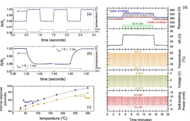
Temperature modulation over time is a well-known methodology to improve the sensor signal in temperature activated devices [102,103]. Pulsed self-heating operation was also demonstrated as a natural extension of the temperature modulated modes [58,59,79]. In the case of self-heating, pulsed operation requires probing the sensor resistance with a specific waveform. In the simplest case, it can be just a train of squared pulses of voltage or current, leading two temperature states: hot and cold. This signal is the most widely used and served to directly measure the thermal response time of the device (Figure 4).
In single wire devices, thermal response times ranging from fractions of microseconds to a few milliseconds have been reported (see Table 1). These values are much faster than those reported for fast MEMS. From a practical point of view, it has been demonstrated that the thermal response times in self-heated nanowires relate to the presence of different gases at different concentrations [59]. In fact, the fast cooling and heating dynamics of self-heated nanowires could be used as a fingerprint to distinguish different gases and observe directly the interaction between the nanowire surface and the gas molecules.
More recently, reports on pulsed operation of large networks of carbon nanofibers revealed a complex structure in the thermal transients, involving several processes of characteristic times ranging from less than 1 millisecond to several seconds [79]. These different processes are still under investigation but seem all related to thermal and gas interaction effects. As a result, certain temperature pulsing modes have already been used to improve the quality of the sensor response, for example, preventing signal drift or accelerating the response time by digital means (Figure 4.d).
Figure 4 (a) Resistance record of a self-heated nanowire operated with a square-pulse bias signal. (b) The resistance changes, due to changes in the nanowire’s temperature, following the bias signal, with response times in the range of 10 ms. (c) These thermal response times depend on the span of the temperature change. Reprinted from Ref. [58], with the permission of AIP Publishing. (d) From a functional point of view, the pulsed operation mode can be used to generate a differential signal (e.g. cold/hot signal) in response to gases. Reprinted from Ref. [79], with permission from Elsevier.
12/29 2.5.3 Other Applications
Although most of the research efforts in self-heated nanowire devices have been focused on conductometric sensors, there are remarkable examples of applications of the self-heating principle to heat up another type of devices, showing that it could be applied to improve energy efficiency in diverse applications [13,64,68,70,72,94–101].
In gas ionization sensors, the chemistry of the working electrode material is used to dissociate gaseous molecules into charged ion species that can be collected and read in a counter electrode [96]. In micron-sized devices based on nanowires, the distance between the electrodes and the shape of the wire, intensifies the ionization field lowering the voltage levels required from kilovolts to a few volts [95]. This fact significantly simplifies the operation of this kind of devices. Still, a heating element is typically needed to trigger the dissociation of certain molecules into ions. It has been reported that sufficiently high temperature can be reached using the self-heating effect in the working electrode nanowire [96].
Self-heating has also been applied to heat up radiation sources. Kim et al. reported on a bridging channel made of a few monolayers of graphene used as a highly efficient infrared light source for optical sensing applications [13]. Sun et al. reported electron emission from CNT arrays operated at over 1700C achieved by means of self-heating [70].
Moreover, thermal effects due to self-heating in nanowires have been investigated to thermally activate memristor behaviors [94], thermoelectricity [64,68], and single wire transistors [72,97–101].
2.6 L
IMITATIONS:
T
HEC
HALLENGE OFI
NTEGRATIONThe first reports on self-heating in nanowires lead to the misconception that the benefits of the self-heating effects (i.e. low power consumption [54], fast thermal response time [58], no need of an additional heater) could only be achieved in devices based on a single nanowire. Consequently, self-heating in nanowires became closely associated to nanofabrication, and to the challenges of gaining electrical access to individual nanowires.
At that point, the community followed mainly two bottom-up strategies: either transferring a fully grown nanowire to a chip, placing it in a certain position, orienting it, and connecting it [52]; or alternatively, attempting the direct growth of the nanowire in the right position in the final chip [12].
Relying on the idea that the minute dimensions of the nanowire were the exclusive responsible for efficient self-heating, Afshar et al. [74] attempted the top-down fabrication of wires based on an In2O3 thin film etched down to form a 100 nm wide conduction channel using laser writing lithography. Despite the resemblance to the single wire scenario, this kind of devices requires much larger amounts of power to exhibit significant heating leading to a valuable conclusion: thermal isolation of the self-heated channel is crucial.
Anyhow, an effective method to produce single-nanowire devices at a wafer scale with high throughput and good reproducibility, is still distant. This fact has systematically discouraged industry from using the self-heating approach.
To circumvent this issue, Chinh et al. thoroughly investigated the self-heating effect in multiple wire systems [71]. Interestingly, they observed that self-heating appeared also in devices based on a few nanowires but being slightly less efficient. This kind of system is relatively simple to fabricate as it is based on the deposition of a few random wires followed
13/29 by a metallization step with conventional lithography methods. However, due to the random nature of the few nanowires involved, the dispersion in the electrical properties and in the self-heating behavior was very large.
To palliate this aspect, Guilera et al. recently reported that the use of dielectrophoresis to orienting the wires between a pair of electrodes contributes to increase the degree of order and reduce the dispersion between samples while keeping efficient self-heating properties [75].
More recent works also show that the self-heating effect can be observed in devices based on large random networks of 1D nanostructures with relatively good efficiencies [78,81], considering the simplicity of the approach. These systems are extremely easy to produce (e.g. by drop casting of nanostructures dispersed in a solvent [78], or just by the direct growth of the 1D-nanomaterials [81]) and exhibit good reproducibility (i.e. in contrast with small arrangements of a few nanowires, these networks contain thousands of wires and they are large enough to offer a macroscopic average of the distribution and properties of the individual nanowires) [77].
According to further investigations, the reason why the temperature of large networks of nanowires can be elevated with a few milliwatts (ESH 10-3) [80,81] is that heat dissipation concentrates in certain regions of the network: the so-called hot spots (see Figure 10.a). In fact, the most effective regions for heat dissipation seem to be the most resistive segments. In other words: the use of 1D nanostructures leads to mesh-like structures that define current paths in which efficient heating is locally possible. Therefore, despite the macroscopic dimensions of the system, ESH figures comparable to those obtained in the moderately efficient nanosystems are possible. From the point of view of the sensing signal, these works also demonstrated that the hot spots are also the ones that generate most of the sensor response, leading to a consistent control of the sensor temperature, precisely in the points relevant for sensing.
3 D
ESIGNINGE
FFICIENTS
ELF-H
EATING:
H
OW-T
O?
The advantages of the efficient self-heating effect in nanowires have already been probed in a broad range of systems and materials. But when it comes to transfer this operating principle to new systems and materials natural doubts arise: how to do it?, to what extend the desired features will be achieved?
This section aims at providing general guidelines for the achievement of efficient self-heating in new materials and system configurations. These suggestions are built upon knowledge available in a broad literature, the own experience of the authors, and finite elements simulations (FEM) carried out specifically to clarify some grey points. To that end, we used the COMSOL Multiphysics software to perform the modeling with the Joule Heating module [104].
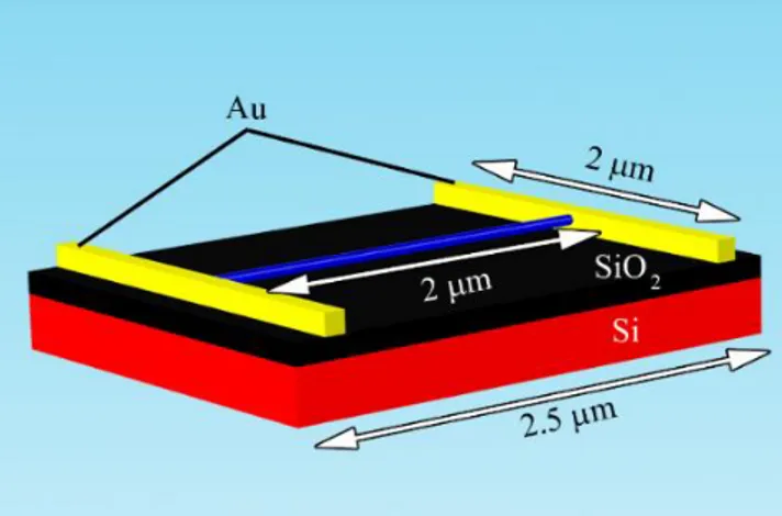
For the sake of simplicity, in this section only an individual suspended nanowire has been considered. The electrical access was made through two gold pads on top of a silicon bulk with a SiO2 insulator layer (Figure 5). Simulation parameters, such as electrical conductivity, thermal conductivity and nanowire dimensions, were selected in a broad range of values, considering most of the materials used in the literature for sensing devices [105–114]. In all cases, a convective cooling boundary condition with a heat transfer of h = 5 W·m-2·K-1 has been applied.
14/29
Figure 5: 3D scheme of the single-wire model between to metal contacts used for FEM simulations.
3.1 M
ATERIALS SHAPE AND DIMENSIONSAs described in the previous section, there are many reports on devices taking advantage of the self-heating effect in nanostructured materials. Today, it is out of question that relatively efficient self-heating can be achieved in typical semiconductor materials (e.g. Si, Ge, GaN), metal oxides (SnO2, ZnO, TiO2, In2O3), carbon allotropes (CNT, CNF, graphene, etc.) if they are shrunk down to the nanoscale in some of their dimensions.
The need for providing a clear and thin path for the current flowing from end to end, along the heated material, suggests a certain preference for 1D (i.e. nanowire, nanotube) or 2D (e.g. graphene) nanostrucutres. In fact, no efficient self-heating effects have been reported for 3D nanoparticles, which typically form aggregates offering thicker current paths.
Concerning sizes, efficient self-heating usually emerges from nanoparticles with characteristic confinement dimensions well below 100 nm. However, as shown in the following sections, this number is strongly dependent on the transport properties of the materials. Still, there is a general trend that suggest that, for the same material and in the same device configuration, the thinner the nanostructure, the higher the heating efficiency (Figure 6). According to our simulations, the increment of the temperature is inversely proportional to the cross-section of the 1D nanostructure being heated. In the case of a cylindric nanowire, this relationship can be written as
∆𝑇 ∝ 1
𝑟𝑛𝑤2 (2)
where rnw is the radius of the nanowire, or in a more general 1D material, any characteristic
15/29
Figure 6 (a) Temperature reached at the center of the nanowire model, and (b) efficient self-heating coefficient (ESH) as a function of the nanowire diameter and the dissipated power with constant thermal and electrical conductivities.
3.2 E
LECTRICAL TRANSPORT PROPERTIESThe fact of measuring the efficiency of the self-heating effect in terms of the electrical power needed to achieve a certain temperature usually leads to the misconception that the efficiency of this heating phenomena is closely related to the electrical transport properties of the materials used (e.g. electrical conductivity). This is, however, not the case.
To illustrate this question we carried out FEM simulations of the self-heating effect in one single nanowire of 2 m in length and 60 nm in diameter bridging between two Au electrodes, considering different electrical conductivities, from = 1 S·m-1 to = 104 S·m-1 and a constant thermal conductivity of = 1 W·m-1·K-1. This range of variation corresponds to typical values of relevant materials, from SnO2 to carbon nanofibers, in a nanostructured form, which is usually higher than their bulk counterparts [105–109]. Figure 7.a clearly shows that, independently on the electrical conductivity, nearly identical temperatures are achieved for the same power consumption (i.e. the same ESH).
However, the electrical transport properties have a major impact on the convenience and practicability of implementing a self-heated device. The electrical conductance determines how the electrical power required for heating must be applied. As illustrated in Figure 7.b, large conductivities involve lower voltages and higher currents. Conversely, low conductivities require lower current levels at a much higher voltage. From the point of view of convenience, the first case might be simpler to implement with conventional electronic components, typically designed for operation in the range of a few volts. Also, the need of higher voltage levels may lead to additional energy losses (e.g. due to the voltage boosting), detrimental for a low power operation mode. Of course, there are also limits on the amount of current that low power devices could provide, but this aspect is usually easier to circumvent with a proper electronic design.
Again, no universal rule seems to exist but, in the authors’ experience, electrical resistances in the range of thousands of ohm provide a good balance in terms of convenience for operation. Beware that this rule of thumbs relates to the macroscopic resistance, which involves not only the conductivity of the material but also its geometrical arrangement. This means that given a material, its final electrical behavior can be adjusted, to some extent by tailoring the device geometry.
16/29
Figure 7: Temperatures reached at the center of the nanowire with different electrical conductivities as a function of (a) the power dissipated, and (b) the voltage applied to a nanowire diameter of 60 nm and a thermal conductivity of κ = 1 W·m-1·K-1. Clearly, given a level of power dissipation, the same temperature is reached, independently of the electrical conductivity of the material. In terms of voltage, higher values must be applied to reach equivalent temperatures, as the material conductivity decreases. The dotted lines connect points operated at the same current value. Therefore, the same current level leads to increasing temperatures, as conductivity decreases.
3.3 H
EAT TRANSPORT PROPERTIESContrary to the case of electric transport, the properties related to heat transport play a crucial role in the effectiveness of the heating.
Figure 8: (a) Temperature reached at the center of the nanowire as function of the power dissipated with different thermal conductivities and (b) efficient self-heating coefficient (ESH) as a function of the thermal conductivity with a nanowire diameter of 60 nm and a electrical conductivity of σ = 100 S·m-1.
Specific simulations, in which the thermal conductivity κ of a nanowire with = 100 S·m -1 was swept from 10-2 to 102 W·m-1·K-1 [110–114] showed that the decrease in κ leads to smaller amounts of electrical power needed to reach the same temperature (Figure 8).
In conventional bulk materials, modifying the thermal conductivity is complex. In contrast, big modifications are relatively simple in nanomaterials, due to the strong influence on the phonon scattering properties of confinement and shape. For example, bulk SnO2 has a thermal conductivity in the range of 50-100 W·m-1·K-1 [110], while its nanometric counterpart can be one or two orders of magnitude lower, 1-5 W·m-1·K-1 [111].
Thus, the modification of the thermal conductivity offers a path for further research in the optimization of heat and electron transport, with the aim of a more efficient heating.
17/29
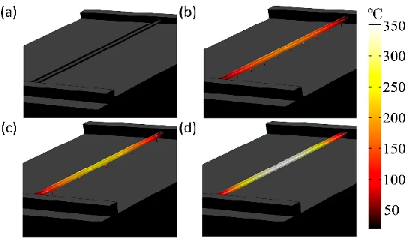
3.4 T
HERMAL LOSES WITH THE SUBSTRATEIn addition to the transport of energy trough the materials under Joule heating, the losses of thermal energy play a fundamental role in the discussion of efficient heating achievement. The early works exploring the effects of Joule heating in thin films (reporting moderate heating with large amounts of power dissipated) suggested [56] and the more recent works, (exploring the possibility of shrinking the conduction path of a thin film in a top-down attempt to build up an energy efficient wire) confirmed [74] that the thermal losses by conduction with the substrate and/or the contacts are the major threat for the self-heating efficiency. To circumvent this problem and optimize the heating efficiency, some authors chose to separate the material from the substrate in suspended configurations [12]. This approach proved to be successfully reaching record power efficiency figures despite the complexity. However, there are also many works showing nanowire-like structures lying apparently in direct contact with a substrate that report efficient heating.
Figure 9: 3D model of the simulated temperature profile along a nanowire with d = 60 nm, σ = 100 S·m-1 and = 1 W·m-1·K-1 in four different scenarios: (a) full flat contact with the substrate; (b) with 10 contact points; (c) with 5 contact points; and (d) fully suspended. A power of 3.7 W was applied in all cases.
To better understand this issue, we carried out again specific FEM simulations adjusting the degree of contact between one single nanowire in self-heating operation and a flat substrate. Detailed studies of the thermal transfer mechanism at the nanoscale [97,98], not only with the substrate but also with the ambience [99], contacts [100,101], etc. are found elsewhere.
Figure 9 shows the thermal behavior in the case of (.a) full flat contact, (.b and .c) discontinuous contact, and (.d) no contact (i.e. suspended wire). In all cases, the same amount of power was dissipated in the wire. Clearly, in accordance with the qualitative trends observed in the experiments, a full an intimate contact between the wire and the substrate hampers all sort of efficient heating. On the other hand, fully suspended nanostructures, even at distances from the substrate as small as 1 nm, show the best results in terms of heating efficiency, as expected from many of the experiments reported elsewhere. Interestingly, the intermediate situations also lead to significant, but lower, temperature increases for the same amount of power (ESH 47, 68 and 88 for the simulations in Figure 9.b, .c and .d, respectively). This last result suggests that, possibly, the contact with the substrate is not complete in devices based on nanowires laying on a substrate. It is plausible thinking that, at such small scale, minor effects like surface roughness, wire bending, etc. easily lead to a discontinued contact scenario.
18/29
3.5 M
ULTIPLEN
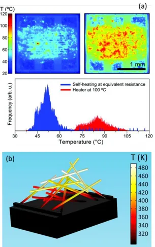
ANOWIRESAs mentioned above, efficient self-heating can also be achieved in systems containing multiple nanowires. Apparently, a network of 1D wires forms a thermal insulating scaffold structure that prevents the direct contact between the substrate and most of the material. This way, the spots in the network that combining sufficient insulation with proper electrical connectivity concentrate most of the heating (Figure 10.a) [65,71,75,77–81]. To illustrate this phenomenon, a structure made of multiple nanowires randomly interconnected has been simulated (Figure 10.b). Clearly, the nanowire portions in direct contact with the substrate reach temperatures well below the ones achieved in the upper nanowire parts. For the sake of comparison, the efficiency of this structure was ESH 32, in contrast with the ESH 88 found for a single nanowire (Figure 9.d). Despite this three-fold reduction of the efficiency, the approach is much simpler to implement and still allows for very low power operation. The questions of how these efficiencies scale with the number of wires in the network and how the network size average out the differences between different random arrangements in different devices are still unanswered, but are crucial to elucidate the future of this approach.
Figure 10: (a) Experimental observations (thermal micrographs) of hot-spots in random networks of CNF operated (left) in heating mode and (right) with an external heater. Clearly, the temperature pattern in self-heating mode concentrates in some central regions of the nanowire network. This is also seen as disperse high-temperature spikes in the blue histogram of the micrographs above, corresponding to the self-heating operation. Reproduced from Ref. [80] with permission from the Royal Society of Chemistry. (b) 3D model of the simulated temperature profile in a random network of nanowires (d = 60 nm, σ = 100 S·m-1, and = 1 W·m-1·K-1) operated at 6.8 W. The nanowire portions in direct contact with the substrate remain cooler than those located further away from the substrate.
19/29
3.6 A
CCURATET
EMPERATUREC
ONTROLThe combination of the heating and the sensing functionalities in one single element entails, however, some additional complexities. In conductometric sensors, the resistance depends both on the gas concentration and the operating temperature,
𝑅(𝑝, 𝑇) = ℱ(𝑇) + 𝒢(𝑝, 𝑇) , (3)
where p stands for the partial pressure of the target gas (i.e. a measure of concentration) and T is the temperature. In eq.(3) we choose to write explicitly two independent contributions to the electrical resistance. On the one hand, ℱ(𝑇) stands for the resistance changes exclusively due to thermal activation. This function could represent the thermal generation of electron-hole pairs in semiconductors, or the electron scattering with lattice phonons in metals; among other phenomena ruling the dependence between electronic transport and temperature. On the other hand, 𝒢(𝑝, 𝑇) stands for the response to gases. These are resistance changes due to the interaction with gaseous molecules. Clearly, this term will depend on the number of molecules p available for the interaction, and on the temperature T at which this interaction occurs as well.
Therefore, the variations of resistance can be expressed in general as 𝑑𝑅(𝑝, 𝑇) = 𝜕ℱ 𝜕𝑇𝑑𝑇 + 𝜕𝒢 𝜕𝑝𝑑𝑝 + 𝜕𝒢 𝜕𝑇𝑑𝑇 = 𝜕𝒢 𝜕𝑝𝑑𝑝 + ( 𝜕ℱ 𝜕𝑇+ 𝜕𝒢 𝜕𝑇) 𝑑𝑇 . (4)
If an external heater is used, the operating temperature can be regarded as a constant, which is fully independent on the materials resistance
𝑇ℎ𝑒𝑎𝑡𝑒𝑟= 𝑐𝑡. (5)
Therefore, eq.(3) is reduced to 𝑑𝑅(𝑝, 𝑇ℎ𝑒𝑎𝑡𝑒𝑟= 𝑐𝑡. ) =
𝜕𝒢
𝜕𝑝𝑑𝑝 , (6)
which is the relationship usually expected in conventional sensors, where the resistance exclusively depends on the presence of gases.
However, in self-heating operation the situation is a bit more complex. In this scenario, the electrical bias point, either a voltage (Vbias) or a current (Ibias), sets the working conditions. This electrical bias dissipates power to heat up the material to a certain temperature, but the power itself depends at the same time on the materials’ resistance. This can be expressed as
𝑇𝑠ℎ(𝑉𝑏𝑖𝑎𝑠= 𝑐𝑡. , 𝑅) or 𝑇𝑠ℎ(𝐼𝑏𝑖𝑎𝑠= 𝑐𝑡. , 𝑅) . (7) Consequently, eq.(4) in the case of self-heating operation results into
𝑑𝑹(𝑝, 𝑇𝑠ℎ) = 𝜕𝒢 𝜕𝑝𝑑𝑝 + ( 𝜕ℱ 𝜕𝑇+ 𝜕𝒢 𝜕𝑇) 𝑑𝑇𝑠ℎ(𝑉𝑏𝑖𝑎𝑠= 𝑐𝑡. , 𝑹) = =𝜕𝒢 𝜕𝑝𝑑𝑝 + ( 𝜕ℱ 𝜕𝑇𝑠ℎ+ 𝜕𝒢 𝜕𝑇𝑠ℎ) 𝜕𝑇𝑠ℎ 𝜕𝑅 𝑑𝑹 (8)
We will not proceed developing eq.(8), as this form is enough to illustrate the discussion about the dependence of the self-heating resistance variations with its own value (bold symbol in eq.(8)).
20/29 According to eq.(8), if a change in the gas concentration dp occurs, this will produce a change in the resistance 𝑑𝑅 that will bring the system towards another operation temperature Tsh. This effect is sometimes argued as a drawback of the self-heating methods: the temperature is unstable because of the resistance variations during sensing.
However, this does not seem to be a true issue in the works reported so far. On the contrary, it is a good strategy to carry out the calibration of the self-heating sensors just by controlling the electrical bias point, without paying much attention to the effective temperature achieved in the devices. In other words, the calibration of the sensor response in constant bias conditions accounts for the temperature variations that may occur because of the presence of gases, and the final sensor outputs are perfectly usable, irrespective of the stability of the true temperature achieved during the experiments. Moreover, this is clearly not a problem in applications of self-heating where no resistive-sensing is needed (e.g. emitters [13,70], transistors [63,72], memristors [94], thermoelectricity [64,68]).
Alternatively, if a behavior similar to the one found with an external heater were needed, it is illustrative to see the dependencies observed in eq.(8). Clearly, to eliminate the dependence on the temperature, and preserve exclusively the dependence on the gas concentration, one could search for a system where 𝜕𝒢 𝜕𝑝⁄ ≫ 𝜕𝑇𝑠ℎ⁄𝜕𝑅. In other words, a system where the variations of the resistance due to temperature were very small, compared to the variations caused by the presence of gases. According to the literature, this is not a rare situation. For example, in carbon-based materials, the resistance variations due to temperature progress at a much slower rate than the response to gases [78] (see Figure 11).
Figure 11: Resistance record of a CNF film operated with self-heating and with an external heater. The variations in temperature due to the resistance variations caused by the gas pulses was estimated to be in the order of 1C. Therefore, the coupling between sensing and heating effects in self-heating operation were nearly negligible in this kind of material. Reproduced with permission from Ref. [78].
In conclusion, it is important to bear in mind the coupling between thermal and sensing effects in self-heating operation, but this is an effect that does not hamper implementing fully functional gas sensors.
21/29
3.7 R
ECOMMENDATIONS FOR ANE
FFICIENTS
ELF-H
EATINGFrom the previous considerations (dimensions, electrical and heat transport properties, and thermal losses), the following conclusions can be drawn:
i. For obvious reasons, the cross-section dimensions of the wires are crucial, as the temperature is inversely proportional to the square of the characteristic width of the nanoparticle (e.g. radius in the case of a cylindrical nanowire).
ii. In terms of materials properties, thermal conductivity is the determining factor for an efficient self-heating. Confinement effects at the nanoscale can modify the thermal conductivity in the direction of improving the efficiency.
iii. The electrical properties (i.e. electrical conductivity or resistivity) are not the key factors to achieve efficient self-heating, but they are accountable for the conditions in which the electrical power should be applied.
iv. Thermal loses with all elements in contact with the self-heated material (usually, substrate and electrical contacts) are greatly detrimental for the efficiency. While some thermal insulation is needed, just a few nanometers might be enough to dramatically reduce these thermal losses.
v. Multiple-wire configuration may help to create the suitable thermal insulation conditions, facilitating device integration, but opening new challenges in device reproducibility.
vi. The coupling between sensing effects and temperature effects on the nanowire resistance affects the amount of power being dissipated. This effect does not compromise the ability to increase the temperature of the material, but limits the accuracy in controlling the actual temperature reached in self-heating mode.
4 C
ONCLUSIONIn this work, we have reviewed the progress made to date in nanowire devices operated with self-heating. It is proposed an objective parameter to quantify and compare the efficiencies achieved in different devices and configurations: the Efficient Self-Heating coefficient. Finally, we compile a set of recommendations (based on own experience, literature, and finite-element simulations) to guide the design of future devices of this kind. After a decade of research, the potential of this approach for lowering the power consumption in temperature-activated sensors has been undoubtfully demonstrated. The future of the approach hangs on our ability to overcome the challenges of integrating one single 1D nanoparticle in an electronic device, or on our ingenuity to recover the same low-power features in much simpler configurations.
5 A
CKNOWLEDGEMENTThe research leading to these results has received funding from the European Research Council under the European Union's Seventh Framework Program (FP/2007-2013)/ERC Grant Agreement n. 336917. J.D. Prades acknowledges the support from the Serra Húnter Program.
22/29
6 R
EFERENCES[1] Clarence W. de Silva, Sensors and Actuators: Engineering System Instrumentation, 2nd ed., CRC Press, 2015.
[2] S. Semancik, R. Cavicchi, Kinetically Controlled Chemical Sensing Using Micromachined Structures, Acc. Chem. Res. 31 (1998) 279–287. doi:10.1021/ar970071b.
[3] S. Semancik, R.E. Cavicchi, M.C. Wheeler, J.E. Tiffany, G.E. Poirier, R.M. Walton, J.S. Suehle, B. Panchapakesan, D.L. DeVoe, Microhotplate platforms for chemical sensor research, Sensors Actuators, B Chem. 77 (2001) 579–591. doi:10.1016/S0925-4005(01)00695-5.
[4] M. Graf, D. Barrettino, H.P. Baltes, A. Hierlemann, CMOS Hotplate Chemical Microsensors, Springer-Verlag, 2007.
[5] I. Elmi, S. Zampolli, E. Cozzani, F. Mancarella, G.C. Cardinali, Development of ultra-low-power consumption MOX sensors with ppb-level VOC detection capabilities for emerging applications, Sensors Actuators B Chem. 135 (2008) 342–351. doi:10.1016/j.snb.2008.09.002.
[6] A. Giberti, V. Guidi, D. Vincenzi, A study of heat distribution and dissipation in a micromachined chemoresistive gas sensor, Sensors Actuators, B Chem. 153 (2011) 409–414. doi:10.1016/j.snb.2010.11.007.
[7] N. Taguchi, Gas-detecting device, 3,631,436, 1971.
[8] D. Briand, A. Krauss, B. Van Der Schoot, U. Weimar, N. Barsan, W. Göpel, N.F. De Rooij, Design and fabrication of high-temperature micro-hotplates for drop-coated gas sensors, Sensors Actuators, B Chem. 68 (2000) 223–233. doi:10.1016/S0925-4005(00)00433-0.
[9] J. Puigcorbé, D. Vogel, B. Michel, A. Vilà, I. Gràcia, C. Cané, J.R. Morante, Thermal and mechanical analysis of micromachined gas sensors, J. Micromechanics Microengineering. 13 (2003) 548–556. doi:10.1088/0960-1317/13/5/304.
[10] T. Iwaki, J.A. Covington, J.W. Gardner, F. Udrea, C.S. Blackman, I.P. Parkin, SQI-CMOS heaters for gas sensors, IEEE SENSORS. 1–3 (2006) 460–463.
[11] S. Vallejos, I. Grácia, O. Chmela, E. Figueras, J. Hubálek, C. Cané, Chemoresistive micromachined gas sensors based on functionalized metal oxide nanowires : Performance and reliability, Sensors Actuators B. Chem. 235 (2016) 525–534. doi:10.1016/j.snb.2016.05.102.
[12] K. Chikkadi, M. Muoth, V. Maiwald, C. Roman, C. Hierold, Ultra-low power operation of self-heated, suspended carbon nanotube gas sensors, Appl. Phys. Lett. 103 (2013). doi:10.1063/1.4836415.
[13] Y.D. Kim, H. Kim, Y. Cho, J.H. Ryoo, C.-H. Park, P. Kim, Y.S. Kim, S. Lee, Y. Li, S.-N. Park, Y.S. Yoo, D. Yoon, V.E. Dorgan, E. Pop, T.F. Heinz, J. Hone, S.-H. Chun, H. Cheong, S.W. Lee, M.-H. Bae, Y.D. Park, Bright visible light emission from graphene, Nat. Nanotechnol. 10 (2015) 1–7. doi:10.1038/nnano.2015.118.
[14] J.R. Stetter, J. Li, Amperometric gas sensors - a review., Chem. Rev. 108 (2008) 352– 366. doi:10.1021/cr0681039.
[15] L. Xiong, R.G. Compton, Amperometric gas detection: A review, Int. J. Electrochem. Sci. 9 (2014) 7152–7181.
23/29 [16] N. Barsan, D. Koziej, U. Weimar, Metal oxide-based gas sensor research: How to?,
Sensors Actuators B Chem. 121 (2007) 18–35. doi:10.1016/j.snb.2006.09.047. [17] A. V., Semiconductor Gas Sensors, Woodhead Publishing Limited, 2014.
doi:10.1016/B978-0-85709-236-6.50018-6.
[18] J. Janata, M. Josowicz, Conducting polymers in electronic chemical sensors, Nat. Mater. 2 (2003) 19–24. doi:10.1038/nmat768.
[19] K.C. Persaud, Polymers for chemical sensing, Mater. Today. 8 (2005) 38–44. doi:10.1016/S1369-7021(05)00793-5.
[20] H. Bai, G. Shi, Gas Sensors Based on Conducting Polymers, Sensors. 7 (2007) 267– 307. doi:10.3390/s7030267.
[21] N.G. Wright, A.B. Horsfall, SiC sensors: a review, J. Phys. D. Appl. Phys. 40 (2007) 6345–6354. doi:10.1088/0022-3727/40/20/S17.
[22] D. Gupta, D. Dutta, P.B. Barman, S. Basu, S.K. Hazra, A Review on Palladium with Low Dimensional Configurations for Chemical Gas Sensor Applications, Sens. Lett. 14 (2016) 211–233. doi:10.1166/sl.2016.3653.
[23] G. Neri, First Fifty Years of Chemoresistive Gas Sensors, Chemosensors. 3 (2015) 1– 20. doi:10.3390/chemosensors3010001.
[24] G. Korotcenkov, Metal oxides for solid state gas sensors : What determines our choice ?, Mater. Sci. Eng. B. 139 (2015) 1–23.
[25] E. Llobet, Gas sensors using carbon nanomaterials: A review, Sensors Actuators, B Chem. 179 (2013) 32–45. doi:10.1016/j.snb.2012.11.014.
[26] N.L.W. Septiani, B. Yuliarto, Review—The Development of Gas Sensor Based on Carbon Nanotubes, J. Electrochem. Soc. 163 (2016) B97–B106. doi:10.1149/2.0591603jes.
[27] D.-S. Lee, J.-H. Lee, Y.-H. Lee, D.-D. Lee, GaN thin films as gas sensors, Sensors Actuators B Chem. 89 (2003) 305–310. doi:10.1016/S0925-4005(03)00008-X. [28] D.M.A. MacKenzie, S.A. Brown, Germanium nano-cluster films as humidity and
hydrogen sensors, J. Appl. Phys. 112 (2012) 2–7. doi:10.1063/1.4758284.
[29] G. Korotcenkov, Practical aspects in design of one-electrode semiconductor gas sensors: Status report, Sensors Actuators, B Chem. 121 (2007) 664–678. doi:10.1016/j.snb.2006.04.092.
[30] P.K. Clifford, D.T. Tuma, The steady state gas sensing characterlstlcs of SnOz gas sensors , as exemplified by the Taguchl Gas Sensor ( TGS ), are comprehensively studied Resistance responses to hydrogen , methane , carbon monoxide and water vapor are experimentally characterized, Sensors and Actuators. 3 (1982) 233–254. [31] P.K. Clifford, D.T. Tuma, Characteristics of semiconductor gas sensors II. transient
response to temperature change, Sensors and Actuators. 3 (1982) 255–281. doi:http://dx.doi.org/10.1016/0250-6874(82)80027-9.
[32] N. Yamazoe, K. Shimanoe, Theory of power laws for semiconductor gas sensors, Sensors Actuators B Chem. 128 (2008) 566–573. doi:10.1016/j.snb.2007.07.036. [33] N. Barsan, U. Weimar, Conduction model of metal oxide gas sensors, J.
Electroceramics. 7 (2001) 143–167. doi:10.1023/A:1014405811371.
24/29 electrochemical gas sensor, Sensors Actuators B Chem. 227 (2016) 185–190. doi:10.1016/j.snb.2015.11.138.
[35] J. Arbiol, A. Cirera, F. Peiró, A. Cornet, J.R. Morante, J.J. Delgado, J.J. Calvino, Optimization of tin dioxide nanosticks faceting for the improvement of palladium nanocluster epitaxy, Appl. Phys. Lett. 80 (2002) 329–331. doi:10.1063/1.1433903. [36] I. Jiménez, M. a. Centeno, R. Scotti, F. Morazzoni, J. Arbiol, A. Cornet, J.R. Morante, NH
3 interaction with chromium-doped WO 3 nanocrystalline powders for gas sensing applications, J. Mater. Chem. 14 (2004) 2412–2420. doi:10.1039/B400872C.
[37] C. Wang, L. Yin, L. Zhang, D. Xiang, R. Gao, Metal oxide gas sensors: Sensitivity and influencing factors, Sensors. 10 (2010) 2088–2106. doi:10.3390/s100302088. [38] A. Kolmakov, M. Moskovits, Chemical Sensing and Catalysis By One-Dimensional
Metal-Oxide Nanostructures, Annu. Rev. Mater. Res. 34 (2004) 151–180. doi:10.1146/annurev.matsci.34.040203.112141.
[39] M.W.G. Hoffmann, A.E. Gad, J.D. Prades, F. Hernandez-Ramirez, R. Fiz, H. Shen, S. Mathur, Solar diode sensor: Sensing mechanism and applications, Nano Energy. 2 (2013) 514–522.
[40] M.W.G. Hoffmann, L. Mayrhofer, O. Casals, L. Caccamo, F. Hernandez-Ramirez, G. Lilienkamp, W. Daum, M. Moseler, A. Waag, H. Shen, J.D. Prades, A Highly Selective and Self-Powered Gas Sensor Via Organic Surface Functionalization of p-Si/n-ZnO Diodes, Adv. Mater. 26 (2014) 8017–8022. doi:10.1002/adma.201403073.
[41] A. Gad, M.W.G. Hoffmann, O. Casals, L. Mayrhofer, C. Fàbrega, L. Caccamo, F. Hernández-Ramírez, M.S. Mohajerani, M. Moseler, H. Shen, A. Waag, J.D. Prades, Integrated Strategy toward Self-Powering and Selectivity Tuning of Semiconductor Gas Sensors, ACS Sensors. 1 (2016) 1256–1264. doi:10.1021/acssensors.6b00508. [42] K. Jenkins, V. Nguyen, R. Zhu, R. Yang, Piezotronic effect: An emerging mechanism for
sensing applications, Sensors (Switzerland). 15 (2015) 22914–22940. doi:10.3390/sl50922914.
[43] M. Belleville, H. Fanet, P. Fiorini, P. Nicole, M.J.M. Pelgrom, C. Piguet, R. Hahn, C. Van Hoof, R. Vullers, M. Tartagni, E. Cantatore, Energy autonomous sensor systems: Towards a ubiquitous sensor technology, Microelectronics J. 41 (2010) 740–745. doi:10.1016/j.mejo.2010.01.009.
[44] B. Martinez, M. Monton, I. Vilajosana, J.D. Prades, The Power of Models: Modeling Power Consumption for IoT devices, IEEE Sens. J. 15 (2015) 5777–5789. doi:10.1109/JSEN.2015.2445094.
[45] N. Yamazoe, Toward innovations of gas sensor technology, Sensors Actuators, B Chem. 108 (2005) 2–14. doi:10.1016/j.snb.2004.12.075.
[46] F. Hernandez-Ramirez, J.D. Prades, R. Jimenez-Diaz, T. Fischer, A. Romano-Rodriguez, S. Mathur, J.R. Morante, On the role of individual metal oxide nanowires in the scaling down of chemical sensors, Phys. Chem. Chem. Phys. 11 (2009) 7105. doi:10.1039/b905234h.
[47] E. Comini, G. Sberveglieri, Metal oxide nanowires as chemical sensors, Mater. Today. 13 (2010) 36–44. doi:10.1016/S1369-7021(10)70126-7.
[48] E. Comini, Metal oxide nanowire chemical sensors: innovation and quality of life, Mater. Today. 0 (2016). doi:10.1016/j.mattod.2016.05.016.