Formation of silicon nanocrystal chains induced via Rayleigh instability in
ultrathin Si/SiO
2
core/shell nanowires synthesized by an inductively
coupled plasma torch process
To cite this article: Marta Agati et al 2019 J. Phys. Mater. 2 015001
View the article online for updates and enhancements.
PAPER
Formation of silicon nanocrystal chains induced via Rayleigh
instability in ultrathin Si/SiO
2
core/shell nanowires synthesized by
an inductively coupled plasma torch process
Marta Agati1,2,3,6 , Simona Boninelli3 , Paola Castrucci4 , Guillaume Amiard3 , Rajesh Pandiyan1 , Gitanjali Kolhatkar1 , Richard Dolbec5 , Andreas Ruediger1
and My Ali El Khakani1,6
1 Institut National de la Recherche Scientifique, Centre-Énergie, Matériaux et Télécommunications, 1650 Blvd. Lionel Boulet, Varennes,
QC, J3X 1S2 Canada
2 Dipartimento di Fisica e Astronomia, Università di Catania, Via S. Sofia 64, Catania, I-95123 Italy 3 CNR IMM, Via S. Sofia 64, Catania, I-95123 Italy
4 Dipartimento di Fisica, Università di Roma‘Tor Vergata’, Via della Ricerca Scientifica 1, Roma, 00133 Italy 5 Tekna Plasma Systems Inc., 2935 Industrial Blvd., Sherbrooke, QC, J1L 2T9 Canada
6 Author to whom any correspondence should be addressed.
E-mail:[email protected]@emt.inrs.ca
Keywords: hybrid nanostructures, Rayleigh instability, inductively coupled plasma, silicon nanowires, silicon nanohybrids
Abstract
A new class of silicon
(Si) nanohybrids is formed exploiting the Rayleigh instability experienced by Si
nanowires
(SiNWs) synthesized via inductively coupled plasma. These nanohybrids consist of three
main categories of Si nanostructures:
(i) core/shell silicon/silicon oxide nanowires (where the inner Si
cores have diameters as small as 2–3 nm), (ii) sequences of almond-shaped silicon nanocrystals
(SiNCs), having diameters in the range of 4–5 nm, connected by an ultrathin silicon nanowire
(diameter of 1–2 nm) and embedded in a silica nanowire, and (iii) sequences of isolated spherical
SiNCs
(having diameters in the range of 4–7 nm) embedded in an otherwise continuous silica
nanowire. The predominance of one morphology over the others can be tuned via post-synthesis
thermal treatments, with a clear predominance of the spherical SiNC chain con
figuration after
high-temperature annealing
(1200 °C). It is demonstrated that the Rayleigh model describes very well the
morphological transformations undergone by the Si core of the nanostructures when subject to the
capillarity-related instability induced by the thermal annealing. More interestingly, we have been able,
for the
first time to our knowledge, to follow in situ the occurrence of Rayleigh instability in SiNWs
leading to the breakage of their inner core and formation of smaller SiNCs. Finally, the optoelectronic
properties of the Si nanohybrids, studied via photoluminescence measurements, have con
firmed the
occurrence of quantum confinement effects in the ultra-small SiNCs present in these new
nanohybrids.
1. Introduction
Silicon(Si) nanostructures have been attracting a renewed interest in recent years because of their quantum confinement (QC)-induced visible light emission. In particular, the system formed by Si nanocrystals (SiNCs) embedded in silica matrix has been designated as a suitable material for optical emission at room temperature [1–3]. On the other hand, ultrathin Si nanowires (SiNWs) have recently shown remarkable optoelectronic properties due to the occurrence of QC effects in these unidimensional nanostructures[4,5]. In the case of inductively coupled plasma(ICP) torch synthesized Si nanostructures, we have recently reported a new class of Si hybrid nanostructures consisting of a random mixture of SiNCs and SiNWs wrapped by a silica shell, which emit strong photoluminescence over the 600–900 nm range [5]. The idea of modulating the size of 0D, 1D, and 2D materials and mixing them to form new nanohybrids has emerged as an original approach to access
enhanced properties or even new functionalities[6–10]. As an example, Heiss et al [8] reported on the controlled
OPEN ACCESS
RECEIVED
7 August 2018
REVISED
28 August 2018
ACCEPTED FOR PUBLICATION
20 September 2018
PUBLISHED
5 November 2018
Original content from this work may be used under the terms of theCreative Commons Attribution 3.0 licence.
Any further distribution of this work must maintain attribution to the author(s) and the title of the work, journal citation and DOI.
synthesis of GaAs quantum dots inside core–shell GaAs/AlGaAs nanowires and their quantum-confinement-induced photoluminescence, which can be efficiently funnelled into a waveguide mode in the nanowire. In the case of Si hybrid nanostructures, few papers have reported the occurrence of mixed SiNCs and SiNWs, where the SiNCs are generated via the periodic instability of the catalyst during the vapor–liquid–solid growth of SiNWs and promoted by the surface oxidization of the SiNWs, or are the result of renucleation and growth direction changes induced by the formation of unfavorable nuclei[11–14]. Another alternative nanostructuring approach, based on the Plateau–Rayleigh assisted growth [15,16], has recently demonstrated the possibility of in situ diameter modulation of SiNWs having initial core diameters of 100 nm[10]. Despite the increasing effort on hybridization of Si nanostructures(generally with the smallest feature of 10 nm and above), the
nanostructuring of ultrathin SiNWs(with diameter of only a few nm and where QC is expected to occur) and their subsequent hybridization with other Si nanostructures via the Rayleigh instability effect have not been reported yet. In fact, the investigation of size-dependent thermal and optoelectronic properties of ultrathin Si nanohybrids has been mainly hindered by the absence of a reliable and reproducible synthesis source of ultrathin SiNWs.
In this paper, we report on the thermal-annealing-induced nanostructuring of ultrathin SiNWs synthesized by means of an ICP-based process[5]. The as-synthesized SiNWs consist of a mixture of ultrathin SiNWs (as thin as 2–3 nm) and SiNCs as small as 3 nm wrapped into a silica nanoshell. By subjecting these core/shell Si/SiO2nanostructures to high annealing temperatures, we were able to achieve novel Si nanohybrids with a
high level of nanostructural order. Indeed, the ICP nanostructures evolve into a system of equally sized SiNCs (with unprecedented ultra-small crystals having sizes of 2–3 nm) periodically placed inside the SiO2NWs as a
result of the Rayleigh instability[15–17]. In fact, while Rayleigh instability theory dates back to the 1800s [15,16], it is widely used for modelingfluid jet instabilities in heterogeneous studies [18], as well as for describing the dewetting of thinfilms induced by laser heating [19,20]. More recently, Rayleigh instability has been applied to investigate instability offilamentary nanostructures and has been effectively used for the synthesis of novel nanocomposites[21–24]. Thus, the Rayleigh instability is shown in the present work to lead to the formation of novel Si nanohybrids, whereby the inner continuous Si core of the SiNWs evolves towards almond-shaped
SiNCs(diameter ∼2–3 nm) connected by a very thin SiNW (∼1–2 nm-diameter) and then into separated
spherical SiNCs(having diameters ranging from 2 to 8 nm) wrapped in an otherwise continuous silica nanocylinder(having an outer diameter in the 10–20 nm range). In these Si hybrid nanostructures, the equally sized SiNCs forming the chain with a regular pitch were found to fairly adhere to the Rayleigh model
expectations. To experimentally demonstrate the formation of these Si nanohybrids induced by the Rayleigh instability, we used state-of-the-art in situ and ex situ transmission electron microscopy(TEM) analyses. The TEM characterizations were mainly exploited in the energy-filtered mode (EFTEM), providing a useful tool to discriminate clearly between the Si core and SiO2shell of the various Si nanohybrids. In particular, the in situ
EFTEM annealing experiments led to the observation, for thefirst time to our knowledge, of real-time transformation of the structure of the Si core of the ICP-SiNWs. These in situ studies were complemented by ex situ annealing experiments on the ICP-SiNWs followed by EFTEM observations. Finally, the blueshifted photoluminescence(PL) of our novel Si nanohybrids confirmed the predominance of QC effects in these
ultra-small SiNCs(with diameters 5 nm as determined from direct EFTEM observations).
2. Methods
The investigated SiNW powder was synthesized by means of an ICP technique commonly used by Tekna Plasma Systems Inc.[25] for the fabrication of Si microspheres [26]. The TEM analyses were accomplished by means of a JEOL JEM 2010F TEM operating at an acceleration voltage of 200 kV and equipped with a Gatan imagefilter (GIF) in order to conduct the analyses in EFTEM mode, selecting the Si plasmon energy loss (17 eV). To perform the in situ TEM analyses, the as-grown SiNW powder was dissolved in isopropyl alcohol, sonicated for about 5 min, and drop-casted onto Si3N4TEM grids, which are resistant up to 1000°C. The sample was in situ
annealed via a heated stage from room temperature up to 990°C. The sample temperature inside the TEM was increased by steps of 200°C every ∼5 min up to 900 °C, then by steps of 15 °C every 4 min until 990 °C was reached. This temperature was then maintained for about 1 h. Focus was put on different regions of the sample in order to observe in real-time the structural changes induced by the heating over time.
Ex situ thermal treatments were performed by annealing the as-grown SiNW powder in a horizontal tube furnace for 1 h under N2flux. The flux of the gas was set at 5 LPM. The powder samples were annealed at
different temperatures ranging from 800 up to 1200°C, dissolved in isopropyl alcohol, sonicated for about 5 min, and drop-casted onto carbon lacey TEM grids for subsequent observations. Statistical EFTEM studies were conducted on each sample through the examination of hundreds of Si nanostructures, in order to evaluate the structural changes as a function of the annealing temperature. Finally, to characterize the optoelectronic
properties of the SiNWs, PL spectroscopy on the annealed samples was performed by means of an AIST-NT
OmegaScope 1000 equipped with a Nanofinder 30 Raman spectrometer and a cooled charge-coupled device
detector, which provides both PL and Raman spectra as well as imaging. For the PL measurements, we used the brightfield configuration by exciting the sample with a green laser (solid-state Cobolt 04-01 series, λ=532.1 nm) focused through a 100×, 0.7 numerical aperture (NA) objective. A 150 lines/mm grating was employed, and the incident power on the samples was equal to 5.4 mW.
3. Results and discussion
3.1. Formation of Si nanohybrids
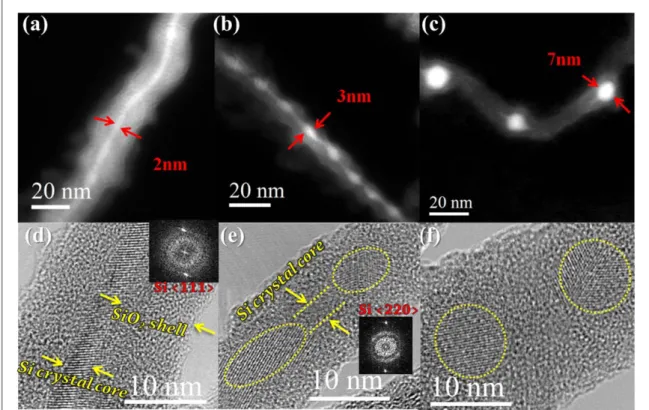
By examining the structural and morphological characteristics of the as-grown ICP-Si nanopowder, we found that three main families of Si nanostructures can be distinguished[5], as shown in figure1:(i) cylindrical SiNWs presenting a rod-shaped Si nanocore(mean diameter of 2.7 nm), as depicted in figure1(a); (ii) chaplet-like SiNWs featuring a chain of almond-shaped SiNCs(mean diameter of 4.5 nm) connected by a very thin Si wire (diameter of 1–2 nm), as illustrated in figure1(b); and (iii) SiNC chains consisting of a sequence of isolated spherical Si nanocrystals(mean diameter of 7 nm) embedded in a continuous SiO2cylinder, as those shown in
figure1(c). The nano-crystalline nature of all these three configurations was ascertained by high-resolution TEM (HRTEM) analyses, as shown in the figures1(d)–(f). In fact, the silicon crystallographic plans are seen in the three respective different configurations: (i) continuous cylindrical crystalline core (figure1(d)), (ii) almond-shaped Si nanocrystals connected by an ultrathin Si nanowire(figure1(e)), and (iii) isolated crystalline Si nanospheres dispersed into an otherwise continuous silicon oxide wire(figure1(f)). The fast Fourier transform (FFT) in the insets of the figures1(d) and (e) corresponds to the very thin crystalline SiNWs, which may feature the cylindrical configuration (figure1(d)) or connect the almond-shaped SiNCs (figure1(e)). The presence of these different families of Si nanostructures in the ICP-synthesized Si nanopowder results, a priori, from the temperature gradient and residence time of the silicon species in the hot plasma region of the ICP torch[27]. In fact, many concomitant phenomena occur during the complex ICP synthesis process, which makes it difficult to single out the effect of the temperature on the synthesized Si nanostructures.
In order to better understand the temperature-related effects on the morphologies of the Si nanostructures, we carried out on-purpose annealing experiments of ICP-SiNWs under two different scenarios:(i) through real-time EFTEM observations of Si nanowires being in situ heated up to a temperature of 990°C; and (ii) via classical
Figure 1.(a)–(c) Typical EFTEM images of the different morphologies of the ICP-synthesized Si nanostructures: (a) cylindrical SiNW, (b) chaplet-like SiNW, (c) SiNC chain. (d)–(f) HRTEM images of the configurations shown in (a)–(c) as evidenced better by the yellow dotted line, which indicates(e) the interconnected almond-shaped particles and (f) the separated spherical particles. The FFTs in the insets of(d) and (e) refer to the very thin crystalline SiNWs.
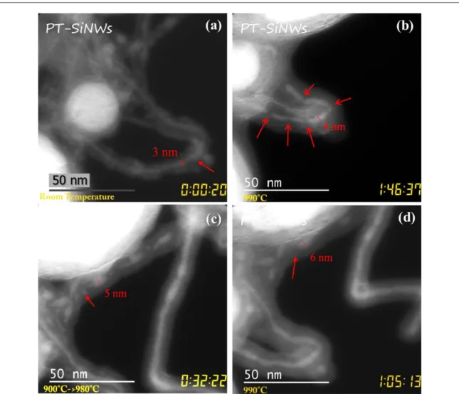
annealing treatments in a furnace at temperatures up to 1200°C. Thus, for the in situ heating of the ICP-SiNWs inside the TEM, the EFTEM images were taken at the plasmon energy loss of Si(17 eV). Figure2(a) shows an EFTEM image depicting a cylindrical SiNW(red arrow) that emerges from a Si nanosphere at the beginning of our observation(initial time t is set = 0, when the sample is still at room temperature). The diameter of the SiNW is of∼3 nm. The EFTEM image of figure2(b) shows the same SiNW after ∼1 h and 45 min of heating, when the temperature reached 990°C. It can be seen that the Si core becomes thinner and breaks at periodic places (indicated by the red arrows), where the fragments (∼4 nm-diameter) are slightly thicker than the Si core of the non-annealed NW, most likely because of atomic diffusion of Si from the breaking points towards the
fragments. Figure2(c) shows another region of the sample after its heating for ∼30 min to reach a temperature of ∼940 °C. This EFTEM image depicts a chaplet-like nanostructure consisting of almond-shaped SiNCs (with a diameter of∼5 nm) connected with a residual ultrathin Si nanowire (red arrow in figure2(c)). After ∼1 h of heating, when the temperature reached 990°C, the ultrathin Si nanowire connecting adjacent SiNCs
disappeared and the almond-shaped SiNCs grew slightly in size(their lateral diameter increased from ∼5 to ∼6 nm when the heating temperature was raised from 940 to 990°C). This enlargement of the SiNCs can be also attributed to the diffusion of Si atoms from the vanishing ultrathin Si nanowire towards the more stable almond-like Si crystals. This heating induced restructuring, observed infigure2(d), leads towards the ultimate formation of spherical SiNC chains; the completion of this transformation may require heating temperatures higher than 1000°C, as will be shown later on. From these real-time, in situ EFTEM observations, it is clearly demonstrated that the annealing temperature can transform the Si inner core of the SiNWs from a continuous cylinder to either chaplet-like SiNWs or spherical SiNC chains. This highlights the important role played by temperature in the morphological evolution of these Si nanostructures. These in situ TEM analyses provided clear evidence of the temperature-induced structural changes of the ICP-SiNWs, suggesting the possible occurrence of a temperature-driven instability in these nanostructures. However, the accessible thermal budget inside the TEM
Figure 2. EFTEM images of(a) cylindrical SiNW at t ∼ 0 and (b) the same SiNW after ∼1 h and 45 min: it can be seen that the SiNW broke up into Si crystalline fragments after the annealing.(c) Chaplet-like SiNW subject to in situ thermal annealing after ∼30 min; (d) the same nanostructure after almost 1 h shows an evolution towards a SiNC chain morphology.
apparatus(990 °C being the highest achievable temperature inside our TEM) is quite likely insufficient to investigate fully the thermally induced transformations.
In order to investigate further these thermally induced nanostructural changes in the ICP-SiNWs, we subjected them to ex situ thermal annealings at temperatures up to 1200°C in a conventional tubular furnace, under N2flux set at 5 liters per minute (LPM) for 1 h, and subsequently examined them by EFTEM. Figure3(a)
illustrates a representative EFTEM image of the samples annealed at 800°C, where one can note the presence of a combination of chaplet-like SiNWs and some SiNC chains, as well as nanowires with continuous cylindrical Si cores. The diameter of continuous cylindrical Si cores was∼3 nm, while that of the almond-shaped SiNCs forming the chaplet-like SiNW or of the spherical SiNCs can vary from 4 to 9 nm. Almost all the observed SiNCs were almond-shaped, with the occasional presence of a residual tail from the vanishing ultrathin connecting Si nanowire. Most interestingly, after annealing the ICP-SiNWs at 1200°C, the spherical SiNC chains were found to be the predominant structure in the sample, as illustrated infigure3(b).
To better account for the effect of annealing on the presence of the three different nanostructure families just defined, statistical analyses were performed on the EFTEM images of both as-grown and annealed ICP-SiNWs. Figures4(a)–(c) show the statistical distributions of the occurrence of the three different SiNW morphologies for the as-grown as well as the annealed ICP-SiNWs at 800 and 1200°C, respectively. It was found that the
cylindrical SiNWs constitute the major component(53% of the overall population) of the as-grown sample, while the percentages of the chaplet-like SiNWs and the SiNC chains represent respectively 35% and 12% of the total nanostructures constituting the as-grown ICP-SiNWs(see figure4(a)) [5]. When the sample was annealed at 800°C, the percentages of both cylindrical and chaplet-like SiNWs decreased to ∼44% and 32%, respectively, while the proportion of SiNC chains increased to 24%(see figure4(b)). This underlines a progressive decreasing of the number of the cylindrical and chaplet-like SiNWs to the benefit of the formation of SiNC chains, as it can be easily inferred from the comparison offigures4(a) and (b). After the 1200 °C annealing treatment, the SiNC
chain nanostructures were found to predominate by accounting for∼77% of the whole SiNW population (see
figure4(c)). This significant increase from 24% (at 800 °C) to ∼77% (at 1200 °C) of the proportion of the SiNC chains occurred to the detriment of the cylindrical and chaplet-like SiNW structures, which only represent ∼13% and ∼10%, respectively, of the 1200 °C annealed sample.
These results clearly confirm that the thermal annealing induces a structural transformation of cylindrical morphologies towards SiNC chains via the chaplet-like configuration, which can be considered as an
intermediate stage. While this structural transformation starts to take place at annealing temperature of ∼800 °C, it accelerates at higher temperatures, as demonstrated by the preponderance of the SiNC chains at 1200°C.
On the other hand, this structural transformation is accompanied by a progressive change in the size of the Si nanostructures, as a result of the annealing-induced atomic diffusion of Si among the nanostructures. To track the annealing-induced variations of the Si nanostructures’ size, direct measurements were taken on numerous EFTEM images for each annealing condition. Figures4(d)–(f) depict the size distributions of the three different Si nanocrystals encountered(i.e., cylindrical, almond-shaped, and spherical SiNCs). It can be seen that the average size of the cylindrical SiNCs(i.e., nanowire diameter) increases from ∼2.7±0.9 nm for the as-grown ICP-SiNWs up to∼8±5 nm in the sample annealed at 1200 °C, while drastically diminishing in proportion (as
shown infigure4(f)). The size distribution of the almond-shaped SiNCs was also found to shift towards a higher mean value upon annealing at 1200°C, as their average diameter increases from ∼4±1 nm for an as-grown sample up to∼5±1 nm for the sample annealed at 1200 °C. Moreover, the spherical SiNCs were found to exhibit a relatively large diameter distribution covering the whole 2–12 nm range (with a mean value around 6±2 nm) after annealing of the ICP-SiNWs at 1200 °C, while their average diameter was around 7±2 nm in the as-grown sample. After annealing at 800°C, the mean diameter of cylindrical SiNWs and almond-shaped and spherical SiNCs are, respectively: 2.5±0.9 nm, 3±1 nm, and 4±2 nm. These results indicate that thermal annealing favors the transformation of the cylindrical SiNWs(having smaller diameters) into chaplet-like SiNWs(as an intermediate step), and then finally towards spherical SiNC chains. The final Si nanostructures (obtained after annealing at 1200 °C) have an average size larger than that of the initial Si cylinders, suggesting that the Si diffuses towards periodic points in the SiNW, where the spherical SiNCs form. Nonetheless, one can notice that even for the sample annealed at 1200°C, there are still some residual cylindrical and chaplet-like
Figure 4.(a)–(c) Statistical distributions of occurrence of the three different SiNW morphologies in (a) as-grown ICP-SiNWs and ICP-SiNWs after annealing in N2at(b) 800 °C and (c) 1200 °C. (d)–(f) Size distributions of the diameters of SiNWs (blue color),
almond-shaped SiNCs(magenta color), and spherical SiNCs (orange color) in (d) the as-grown sample and in the samples annealed in N2at(e) 800 °C and (f) 1200 °C.
SiNWs having diameters larger than in the non-annealed samples. This indicates that higher annealing temperatures are required to fully transform those residual SiNWs into spherical SiNCs.
3.2. Rayleigh instability model
The results of both in situ heating and ex situ post-annealing analyses pointed out that the observed
nanostructures in the ICP-SiNWs are the result of a thermally driven phenomenon. In fact, the transformation of cylindrical nanostructures towards a periodic succession of spherical nanoparticles is explained in literature in terms of the phenomenon of Rayleigh instability[22,28,29]. This phenomenon is more generally due to perturbations of cylindricalfluids generating a capillarity-related instability and, eventually, leading to the fluid thread breakup[18]. Indeed, during the analysis of the instability phenomena in fluid threads, Plateau [15] found that the shape of cylindricalfluids becomes unstable under the influence of surface tension at elevated temperatures. By considering such thermally induced perturbations as the convolution of sinusoidal components characterized by their different wavelengths[15], Plateau demonstrated that the unstable perturbations have wavelengths(λm) such that λm>2πR0, where R0is the radius of the initial cylinder(more
details about the mathematical demonstration are reported in ref.[18]). The peak and trough of each sinusoidal component of the perturbation induce a disturbance at the surface of the cylinder with periodically positive and negative curvatures, thus forming pinched sections with higher pressure and bulging sections with lower pressure. At enough high-pressure gradient, thefluid flows from the pinched sections towards the bulged ones, leading to a more stablefinal state in which the cylinder breaks up at the pinched points. Rayleigh demonstrated that there is a specific perturbation with wavelength l that grows exponentially with respect to the others, and thus induces the breakup of the cylinder into spherical droplets at periodic points[16]. A schematic
representation of the three main structural transformation steps of the Rayleigh instability process is given in figure5(a). As demonstrated by Nichols and Mullins [17], a perturbation ruling the surface diffusion of atoms along the initial cylinder from the pinched regions towards the bulged ones is described by the wavelength l given in equation(1):
l= 2 2pR0=8.89R0. ( )1
The diameter of the resulting spherical droplet has been estimated by Muller et al[30]:
l
= = = ( )
D 2R 36 R0 3.78R0. 2
As a result, the ratiol/R, where R is the radius of thefinal spherical droplets and l is the inter-distance between them, is:
l/ R=constant 4.7.= ( )3
Hence, the Rayleigh instability induces the formation of chains of regularly spaced spheres with the same diameter, which basically depends on the radius of the initial cylinder, and where both the distance between the spheres and their size obey the mathematical relationship described in equation(3).
In order to ascertain that the Rayleigh instability was responsible for the thermally induced morphological
transformation observed in our annealed ICP-SiNWs, we compared the experimentalλ/R ratio of our SiNW
samples with the theoretical value predicted by the Rayleigh model. Thus, for each annealing condition, we have systematically measured the diameters of the SiNCs(both almond- and spherical-shaped) and their inter-distanceλ on the numerous EFTEM images (as illustrated in figure5(b)). About 100 (R, λ) pairs were measured for each annealing condition. The results of this analysis are represented infigure5(c), which displays the λ/R ratio as a function of the annealing temperature. It is worth noting that theλ/R value obtained for the as-grown SiNWs and even for those annealed up to 800°C is ∼10 (still far from the theoretical value of ∼4.7), indicating that the Rayleigh instability was still far from being fully activated at 800°C. The λ/R ratio reaches its lowest value of 5.2±0.4 at 1200 °C annealing temperature. In order to interpolate the data between 800 °C and 1200 °C, we performed a further annealing at 1000°C, which gave a value of the λ/R ratio equal to 8±0.4. The λ/R ratio at 1200°C, being 5.2±0.4, is comparable with the theoretical value (within the statistical margin), indicating that the structural transformation in ICP-SiNWs was driven by the Rayleigh instability for annealing temperatures 1200 °C. The presence of some residual cylindrical and chaplet-like SiNWs at 1200 °C is believed to be due to their relatively larger diameters(figure4(f)), which would require higher temperatures to activate their full conversion into SiNCs. This has been indeed reported in previous works, where the Rayleigh instability phenomenon was found to occur at higher temperature for larger nanowire diameters[22,29]. In conclusion, these results confirmed that the annealing treatments of the ICP-SiNWs induced a progressive thermal instability starting from 800°C and reaching the Rayleigh instability condition at 1200 °C, where the SiNWs were almost fully transformed into regular chains of SiNCs according to the just-outlined Rayleigh–Plateau model.
3.3. Optoelectronic characterization
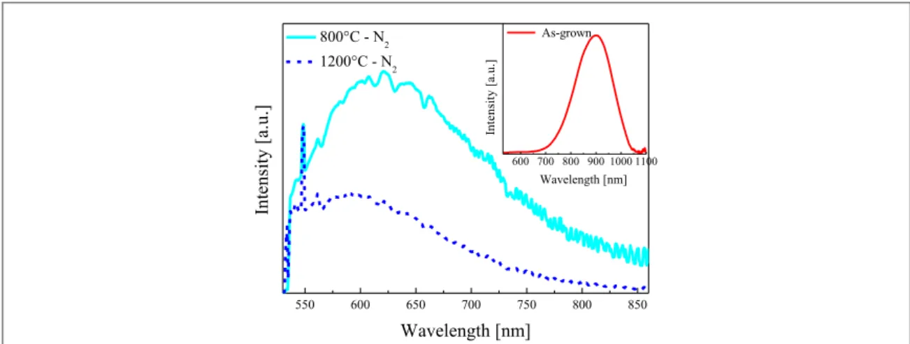
Finally, the optoelectronic properties of the ICP-SiNWs were characterized by means of PL spectroscopy. Figure6displays the PL spectra of the samples annealed at 800° and 1200 °C under N2flux, as well as the PL of
the as-grown sample for comparison[5]. For the as-grown sample, the PL emission of the Si nanohybrid structures, the sizes of which were revealed by EFTEM observations and presented infigure4(d), was found to be characterized by a wide emission band spanning over the 620–1000 nm range. This visible light emission is a clear indication of the occurrence of QC in these different Si nanostructures(bulk silicon is known to have an indirect bandgap in the IR around 1100 nm). This PL peak shifts towards shorter wavelength (∼620 nm) after annealing at 800°C (see figure6). This additional QC-induced blueshifting of the PL peak is attributed to the dimension reduction of the emitting Si nanocrystals. Indeed, the cylindrical Si nanostructures evolve at 800°C in a sequence of very small almond-shaped SiNCs(mean size of 3 nm, as discussed previously and evidenced in figure4(e)), connected by ultrathin SiNWs. These cylindrical and chaplet SiNWs are still predominant at 800 °C. On the other hand, the spherical SiNCs have rather comparable size in the as-grown sample and in the sample annealed at 800°C, as discussed previously. The PL peak of the 1200 °C annealed ICP-SiNWs is located around 590 nm, while its intensity decreases with respect to the PL of the sample annealed at 800°C. The optical emission at such short wavelength may sound contradictory with the general tendency discussed before, where increasing the annealing temperature from 800 to 1200°C was found to increase the average size of the SiNCs. In fact, at 1200°C, the majority of the Si nanostructures is represented by spherical SiNC chains, of which the sizes cover the 2–12 nm range (and where SiNCs having size larger than the Bohr radius of 5 nm are not expected to emit any PL). This indicates that the oxygen-based defects may contribute to the light emission of our ICP-SiNWs. Indeed, bridging oxygen-hole centers in silica NWs were reported to be responsible for the PL emission in the 620–650 nm spectral range [31]. However, such oxygen-based defects are expected to heal with annealing
Figure 5.(a) Schematic diagram of the Rayleigh instability mechanism. (b) HRTEM image of a SiNC chain where the physical quantitiesλ and R are illustrated. (c) Variation of the λ/R ratio of the ICP-SiNWs as a function of the annealing temperature. At 1200°C, the value of λ/R approaches the theoretical value of 4.7, represented here by the red dashed line.
treatments, particularly at temperatures higher than 1050°C [32]. In fact, for the ICP-SiNWs annealed at 1200°C, the PL component located at 650 nm has very low intensity, suggesting that the major part of the oxygen defects were indeed healed. In addition to the quantum-confinement-induced PL (expected for Si nanocrystals having a size5 nm), spatial confinement in nanosized crystals (larger than 5 nm) can also contribute to the PL emission of silicon nanostructures[33]. In fact, the long exciton lifetime (μs-ms) in a spatially confined volume (Si nanocrystals with diam. Bohr radius) favors the PL emission to the detriment of non-radiative recombination. Nevertheless, a more comprehensive and detailed analysis is still needed to better understand the photoluminescence of these Si nanohybrid materials and its blueshift upon annealing.
4. Conclusion
The formation of new Si-based nanohybrids was demonstrated via high-temperature thermal annealing of ultrathin core/shell Si/SiO2nanowires synthesized via an ICP-based process[5,34,35]. The formation
mechanisms of these Si hybrid nanostructures was described on the basis of instability phenomena undergone by the inner Si core of the ICP-SiNWs when subjected to high-temperature annealing conditions. These thermally induced instabilities are shown to lead to the shrinking of the SiNWs’ core at periodic places or their breaking into fragments(having ultimately a spherical shape), in accordance with the Rayleigh model. In this case, three main morphologies of the inner Si core have been identified, namely cylindrical SiNWs, chaplet-like SiNWs, and SiNC chains(where the size of adjacent spherical SiNCs and their inter-distance obey the Rayleigh λ/R ratio). The chaplet-like SiNW configuration represents the intermediate step in the transition from the cylindrical Si core to the SiNC chainfinal state. Retrospectively, these results suggest that the different Si nanostructures observed in the as-grown ICP-SiNWs are due to the Rayleigh instability that affects the nanowires in the ICP reactor known for its high temperature gradient. Thus, the ICP-SiNWs can undergo different temperature gradients and residence times in the hot plasma zone of the reactor, which will favor the development of one of the three stadia of the Rayleigh instability. Finally, the PL spectra of the annealed ICP-SiNWs showed a clear blueshift which could be attributed to the occurrence of QC in these nanostructures as long as their size remains5 nm. Nevertheless, in addition to the QC-induced PL for smaller nanostructures, the overall PL emission of such Si nanohybrids can also originate from other effects such as oxygen defects in the surrounding silica layer and/or from spatial confinement in Si nanostructures larger than the Bohr radius.
Acknowledgments
The authors would like to acknowledge support from the Italian Ministry of Foreign Affairs and International Cooperation, Directorate General for the Promotion of the Country System. Most of this work was performed at
Beyondnano CNR-IMM, which was supported by the project Beyond-Nano(PON a3_00363). The authors
would also like to acknowledgefinancial support from the Natural Sciences and Engineering Research Council (NSERC) of Canada through the Discovery grants program, and the FRQNT (Le Fonds de Recherche du Québec-Nature et Technologies) through its strategic Network ‘Plasma-Québec’. Finally, the authors would like to thank Dr. Francesco Ruffino for interesting discussions about his previous works on Rayleigh instability.
Figure 6. PL spectra of ICP-SiNWs annealed at 800°C (cyan line) and 1200 °C (blue dashed line). In the inset, the PL of the as-grown SiNWs is shown for comparison(red line). Reproduced from [5].CC BY 4.0.
Con
flict of interest
The authors declare no conflict of interest.
ORCID iDs
Marta Agati https://orcid.org/0000-0002-2108-4800
Paola Castrucci https://orcid.org/0000-0001-8986-7185
Gitanjali Kolhatkar https://orcid.org/0000-0003-0848-4751
References
[1] Iacona F, Bongiorno C, Spinella C, Boninelli S and Priolo F 2004 Formation and evolution of luminescent Si nanoclusters produced by thermal annealing of SiOxfilms J. Appl. Phys.95 3723
[2] Boninelli S, Iacona F, Franzò G, Bongiorno C, Spinella C and Priolo F 2005 Thermal evolution and photoluminescence properties of nanometric Si layers Nanotechnology16 3012
[3] Franzò G, Miritello M, Boninelli S, Lo Savio R, Grimaldi M G, Priolo F, Iacona F, Nicotra G, Spinella C and Coffa S 2008 Microstructural evolution of SiOxfilms and its effect on the luminescence of Si nanoclusters J. Appl. Phys.104 094306
[4] Irrera A, Artoni P, Iacona F, Pecora E F, Franzò G, Galli M, Fazio B, Boninelli S and Priolo F 2012 Quantum confinement and electroluminescence in ultrathin silicon nanowires fabricated by a maskless etching technique Nanotechnology23 075204
[5] Agati M, Amiard G, Le Borgne V, Castrucci P, Dolbec R, De Crescenzi M, El Khakani M A and Boninelli S 2016 Growth mechanisms of inductively-coupled plasma torch synthesized silicon nanowires and their associated photoluminescence properties Sci. Rep.6 srep37598
[6] Peng K Q, Wang X, Wu X L and Lee S T 2009 Platinum nanoparticle decorated silicon nanowires for efficient solar energy conversion Nano Lett.9 3704
[7] Ka I, Le Borgne V, Ma D and El Khakani M A 2012 Pulsed laser ablation based direct synthesis of single‐wall carbon nanotube/PbS quantum dot nanohybrids exhibiting strong, spectrally wide and fast photoresponse Adv. Mater.24 6289
[8] Heiss M et al 2013 Self-assembled quantum dots in a nanowire system for quantum photonics Nat. Mater.12 439
[9] De La Mata M, Zhou X, Furtmayr F, Teubert J, Gradečak S, Eickhoff M, Fontcuberta i Morral A and Arbiol J 2013 A review of MBE grown 0D, 1D and 2D quantum structures in a nanowire J. Mater. Chem. C1 4300–12
[10] Day R W, Mankin M N, Gao R, No Y S, Kim S K, Bell D C, Park H-G and Lieber C M 2015 Plateau–Rayleigh crystal growth of periodic shells on one-dimensional substrates Nat. Nanotechnol.10 345
[11] Kohno H and Takeda S 1998 Self-organized chain of crystalline-silicon nanospheres Appl. Phys. Lett.73 3144–6
[12] Wang N, Tang Y H, Zhang Y F, Lee C S and Lee S T 1998 Nucleation and growth of Si nanowires from silicon oxide Phys. Rev. B58 R16024
[13] Kohno H, Takeda S and Tanaka K 2000 Plasmon-loss imaging of chains of crystalline-silicon nanospheres and silicon nanowires J. Electron Microsc.49 275–80
[14] Kohno H and Takeda S 2005 Chains of crystalline-Si nanospheres: growth and properties e-J. Surf. Sci. Nanotech.3 131–40
[15] Plateau J A 1873 Statique Expérimentale Et Theorique Des Liquides Soumis Aux Seules Forces Moléculaires (vol 2) (Paris: Gauthier-Villars) [16] Rayleigh L 1878 On the instability of jets Proc. London Math. Soc.10 4–13
[17] Nichols F A and Mullins W W 1965 Surface-(interface-) and volume-diffusion contributions to morphological changes driven by capillarity Trans. Metall. Soc. AIME 233 1840
[18] Eggers J and Villermaux E 2008 Rep. Prog. Phys.71 036601
[19] Wu Y 2011 Nanoscale metal thin film dewetting via nanosecond laser melting: understanding instabilities and material transport in patterned thinfilms PhD Thesis University of Tennessee (http://trace.tennessee.edu/utk_graddiss/1240)
[20] Ruffino F, Carria E, Kimiagar S, Crupi I and Grimaldi M G 2013 Rayleigh-instability-driven dewetting of thin Au and Ag films on indium–tin–oxide surface under nanosecond laser irradiations Micro Nano Lett.8 127
[21] Karim S, Toimil-Molares M E, Balogh A G, Ensinger W, Cornelius T W, Khan E U and Neumann R 2006 Morphological evolution of Au nanowires controlled by Rayleigh instability Nanotechnology17 5954
[22] Qin Y, Lee S M, Pan A, Gösele U and Knez M 2008 Rayleigh-instability-induced metal nanoparticle chains encapsulated in nanotubes produced by atomic layer deposition Nano Lett.8 114
[23] Qin Y, Vogelgesang R, Eßlinger M, Sigle W, van Aken P, Moutanabbir O and Knez M 2012 Bottom‐up tailoring of plasmonic nanopeapods making use of the periodical topography of carbon nanocoil templates Adv. Funct. Mater.22 5157
[24] Xu J, Zhu Y, Zhu J and Jiang W 2013 Ultralong gold nanoparticle/block copolymer hybrid cylindrical micelles: a strategy combining surface templated self-assembly and Rayleigh instability Nanoscale5 6344
[25] Teknawww.tekna.com(Accessed June 2018)
[26] Guo J Y, Gitzhofer F and Boulos M I 1995 Induction plasma synthesis of ultrafine SiC powders from silicon and CH4 J. Mater. Sci.
30 5589
[27] Guo J, Fan X, Dolbec R, Xue S, Jurewicz J and Boulos M 2010 Development of nanopowder synthesis using induction plasma Plasma Sci. Technol.12 188
[28] Toimil-Molares M E, Balogh A G, Cornelius T W, Neumann R and Trautmann C 2004 Fragmentation of nanowires driven by Rayleigh instability Appl. Phys. Lett.85 5337
[29] Rauber M, Muench F, Toimil-Molares M E and Ensinger W 2012 Thermal stability of electrodeposited platinum nanowires and morphological transformations at elevated temperatures Nanotechnology23 475710
[30] Müller T, Heinig K H and Schmidt B 2002 Template-directed self-assembly of buried nanowires and the pearling instability Mater. Sci. Eng. C19 209–13
[31] Shang N G, Vetter U, Gerhards I, Hofsäss H, Ronning C and Seibt M 2006 Luminescence centres in silica nanowires Nanotechnology
17 3215
[32] Jambois O, Rinnert H, Devaux X and Vergnat M 2006 Influence of the annealing treatments on the luminescence properties of SiO/SiO2multilayers J. Appl. Phys.100 123504
[33] Ross G G, Barba D and Martin F 2008 Structure and luminescence of silicon nanocrystals embedded in SiO2Int. J. Nanotechnol.5
984–1017
[34] Agati M, Amiard G, Le Borgne V, Castrucci P, Dolbec R, De Crescenzi M, El Khakani M A and Boninelli S 2017 Self-assembly of silicon nanowires studied by advanced transmission electron microscopy Beilstein J. Nanotechnol.8 440–5
[35] Le Borgne V, Agati M, Boninelli S, Castrucci P, De Crescenzi M, Dolbec R and El Khakani M A 2017 Structural and photoluminescence properties of silicon nanowires extracted by means of a centrifugation process from plasma torch synthesized silicon nanopowder Nanotechnology28 285702

![Figure 6 displays the PL spectra of the samples annealed at 800° and 1200 °C under N 2 flux, as well as the PL of the as-grown sample for comparison [5]](https://thumb-eu.123doks.com/thumbv2/123dokorg/7576337.112096/9.892.184.828.90.687/figure-displays-spectra-samples-annealed-flux-sample-comparison.webp)