DOTTORATO DI RICERCA IN
FISICA
CICLO XXII
COORDINATORE Prof. Filippo Frontera
Manipulation of charged particle beams
through coherent interactions with crystals
Settore Scientifico Disciplinare FIS/01
Dottorando Tutore
Index
1. Coherent interactions between charged particles and crystals 1.1. Channeling
1.2. The continuum potential approximation
1.3. Particle motion in the field of atomic planes and axes 1.3.1. Motion under planar channeling
1.3.2. Motion under axial channeling 1.4. Motion in a bent crystal
1.5. Volume Reflection (VR) and Volume Capture (VC) 1.6. Multiple Volume Reflection in One Crystal (MVROC) 1.7. References
2. Fabrication and bending of crystals for channeling 2.1. Strip like crystals fabrication
2.1.1. Isotropic etching
2.1.2. RBS and Channeling-RBS 2.1.3. RBS-Channeling
2.2. Anisotropic etching 2.3. Crystal bending
2.3.1. Anticlastic deformation in an anisotropic material 2.3.2. Simulation and experimental
2.3.3. Holders for strips and multi-strips crystals. 2.4. A crystals for low energy negative particles channeling 2.5. References
3. Coherent interactions between positively charged particles and crystals 3.1. The experimental setup
3.1.1. Silicon microstrip detectors 3.1.2. The goniometer
3.2. Setting up
3.2.1. Crystal pre-alignment 3.2.2. Lateral alignment 3.2.3. Torsion compensation
3.3. Planar channeling in short bent crystals.
3.4. Deflection of 400 GeV proton beam by means of axial channeling 3.5. Single volume reflection in a single crystal
3.6. Volume reflection dependence on crystal bending radius 3.7. Multiple volume reflections
3.7.1. Multiple volume reflections in QM-like crystals 3.7.2. MVR in multistrip crystals
3.7.3. Multiple volume reflection in a single crystal 3.8. Discussion
4.2. Deflection of negative particles by axial channeling 4.3. Emission of radiation in the VR process
4.3.1. Radiation from bent crystals 4.3.2. Experimental setup
4.3.3. The spectrometer method 4.3.4. The amorphous contribution 4.3.5. VR Spectra
4.4. Discussion 4.5. References
Introduction
In the last years, the field of channeling and related phenomena aimed to particle-beam steering has received a tremendous impulse by the advent of a new generation of silicon crystals, which resulted in significant performance increase and lead to the discovery of novel phenomena.
The first key factor was the usage of silicon crystals exploiting secondary deformations, which provide extremely uniform bending an optimal sample thickness across the beam. Moreover, the holder to impart the primary curvature is designed to keep apart all the material but silicon from the trajectory of the beam.
A second key factor which lead to performance improvement is the quality of the crystal surfaces by using properly tailored chemical etchings. In particular, the entry face of the crystal plays an important role, because it is the surface accepting incoming beam particles.
Lastly, significant contribution was due to the characterization of the samples with a variety of techniques. A thorough characterization allows fine adjustment of the experimental parameters for crystal fabrication and certification of its quality prior to installation in the accelerator.
In this thesis it will be shown the procedures for manufacturing of crystal realized at Sensors and Semiconductor Laboratory of Ferrara University. The fabrication methods, based on revisitations of micromachining techniques, allow obtaining high quality crystals, which lead to performance increase as well as to the discovery of new effects in the interaction with positively and negatively charged particle beams at CERN facilities.
As it will be shown in this thesis, the geometry and the quality of the realized crystals allowed attaining a record 83% efficiency when operated to deflect a 400 GeV proton beam at the H8 line at CERN by means of planar channeling and contributed to the observation of volume reflection.
The same crystal generation enabled to observe multiple volume reflection in both a series and in a single crystal and to successfully achieve deflection of negatively charged particle beams through either channeling or volume reflection.
Coherent phenomena in crystals may be the basis for halo collimation for current hadron colliders (e.g. the LHC). An efficient collimation system is a necessary condition to run the accelerator at its top luminosity and to prevent damage of its sophisticated superconductive magnets. This smarted collimation scheme is currently being under investigation in the pilot UA9 experiments, which investigate crystal-assisted schemes for halo collimation in the CERN SPS through channeling of protons. The first and preliminary results of UA9 experiment shows good perspectives on the possibility to collimate the LHC beam by using bent crystals.
Chapter 1
Coherent interactions between charged particles and crystals
1.1. ChannelingA large variety of physical phenomena may occur in interaction between charged particles and matter. For example Rutherford scattering, energy loss, nuclear reactions, x-ray production etc…If the target material is homogenous and isotropic the impact parameter of any interaction is independent of the orientation between particle beam and target. When the target material is monocrystalline the yields of physical processes and the impact parameters are function of orientation between target and particle beam. This is due to the so called “channeling” effect. From an intuitive point of view if the particle impinge on the crystal not so close to the atomic planes, in order to prevent strong interaction with nuclei, and with direction close to planes (planar channeling ) or an axis (axial channeling), with high probability it will be subject to correlated scattering events on the atomic planes. Because of the periodic crystal structure the particle will undergo a series of small-angle collisions, resulting in a steering effect which causes the particle to oscillate between atomic planes or wander among crystal axis, leading to a reduction of close-encounter related events.
Channeling was discovered during low energy ions implantation and by computer [1.1]simulations, which consider this effect as unwanted because it alters the desiderate ions implantations profile and then theoretically studied by Lindhard [1.2] and experimentally beams from Van der Graaf accelerators as tools for materials characterization[1.3]. Based on the ideas from Tsyganov [1.4] to deflect high energy particles beam using bent crystals, high energy channeling have been investigated by different institutes in USSR, USA, CERN. Apart from the possibility to deflect high energy particle beam, different subjects have been Figure 1.1: schematic representation of planar channeling
1.2. The continuum potential approximation
The potential describing the interaction between an ion (atomic number Z1) and an isolated atom (atomic number Z2) can in general be expected to be a quite complicated function of several parameters such as the masses, the distance between ion and atom, the relative velocity, the atomic numbers and the impact parameter. In order to simplify the problem it is usual to assume a two-body like interaction and it is neglected any velocity dependence of the atom-ion interaction potential. This is a reasonable assumption keeping in mind that channeling interactions are “gentle” small-angle. Under such assumption the interaction can be described by a static potential similar to the one of diatomic molecules. This still remain a complex problem to be treated theoretically, involving a Hartree-Fock approach. In order to further simplify the ion-atom potential a well working approximation consist in modeling the interaction potential following the Thomas-Fermi model, where the interaction potential is given by
2 ( ) i TF Z Ze r V r r a (1.1)
Here r is the distance between the particle and the atom, 1/ 3 0 1 2
0.8853 ( )
TF
a a Z Z and
a0 is the Bohr radius. The term
r a/ TF
is a screening function which takes into account the charge distribution of the atom. The Thomas-Fermi approach cannot take into account such detailed features as electronic shell structure of the atoms, but it is a good approximation to Hartree-Fock calculations. A widely used analytical form for is given by Molière [1.26]
3 1 / i TF r a TF i i r a e
(1.2) ,where α=(0.1;0.55;0.35) and β=(6.0;1.2;0.3). An alternative form for is given by Lindhard [1.2],
1/ 2 2 / TF 1 1 Ca r a r (1.3)Where C is a standard constant with value of 3.
From a classical point of view a particle is channeled if it is incident on the row or plane at an angle below the “critical angle”, i.e. an angle small enough so as not to feel the individual atom potential, but an averaged one[1.27]. Lindhard showed [1.2] that for incidence close to an axis (axial channeling) this angle is given by 2 1/ 2
1 2
(2 / )
a Z Z e dE
while for incidence close to a plane (planar channeling) we have 2 1/ 2 1 2
(2 / )
p nZ Z e a E
where d is the spacing in the atomic row, E is the particle energy, n the atomic areal density. Under this assumption we may consider the motion of the particle as the motion in an averaged potential. Considering a particle at distance ρ from an atomic row we have
w h e r e 2 2 1/ 2 (x R )
is the distance between the ion and an atom of the plane, see Fig. [1.2].
The potential experienced by the ion will be the sum of the potentials of all the atomic rows in the axial channeling regime, and of all the planes in the planar mode. Axial potential is the total potential at a point r in the plane normal to the axis, i.e.
min
( ) ( )
R R i R
i
U ρ
V r ρ U (1.6)where ρi are the positions of the atomic rows measured in the plane normal to the axis and
min
R
U is a constant subtracted in order to make the minimum value of U ρ equal to zero. For R( ) the planar potential we have
min
( ) ( )
P P P
i
U x
V r x i U (1.7)In Fig [1.3] the planar and axial potentials for silicon for planes (110) and axis <111> respectively are represented.
2 2 1/ 2 1 [( ) ] V V x dx d
(1.4)while for the planar case we have
2 2 1/ 2 0 ( ) 2 ( ) P V x n RV x R dR
(1.5)Figure 1.2: a collision of channeled particle with axis (a) or plane (b)
1.3. Particle motion in the field of atomic planes and axes
Channeled particles travels at small angles with respect to atomic rows or planes, so interactions with atoms of the crystal may be consider as elastic. Neglecting energy losses the longitudinal component of the momentum may be treated as constant.
1.3.1 Motion under planar channeling
Let’s consider as first the motion of a particle under planar channeling moving in the potential U(x), we have:
E p c2 2x p cz2 2m c2 4 U x( )const Eq (1.2)
Remembering that the angle θ=px/pz is small, we may write
2 2 ( ) 2 x z z p c U x E const E Eq (1.3)
whereEz p cz2 2m c2 4 . The sum of the first two terms of the last relation is often regarded as “transverse energy” in the literature. Since pz is constant it is easy to show that transverse energy is
conserved, i.e. 2 2 2 2 2 ( ) ( ) 2 2 x z T z z p c p c E U x U x const E E Eq (1.4)
Assuming Ez and remembering that E pc2 vEwhere v is the particle velocity, we have
2 ( ) 2 T pv E U x const Eq (1.5) Considering that x x x z z z p v d p v d Eq (1.6)
for any potential U(x) we may calculate the particle trajectory integrating the equation 2 [ T ( )] dx dz E U x pv Eq (1.7)
Differentiating (1.7) with respect to z we obtain
2
2 '( ) 0
d x
pv U x
dz Eq (1.8)
approximating the U(x) potential with an harmonic shape
2 0 2 ( ) h p x U x U d Eq (1.9)
0 2 sin 2 2 2 cos p T T d E z x U E z pv Eq (1.10) with 0 2 p pv d U Eq (1.11)
In planar channeling particles regime oscillates between atomic planes, for example for channeling among (110) silicon planes the oscillation period has an average value of 58 µm at 400 GeV.
During the passage through the crystal, some particles may leave their bound states due to multiple Coulomb scattering both on the nuclei (MSN) and electrons (MSE) of the crystal atoms (dechanneling process). The particle scattering on the crystal nuclei occurs in a “nuclear corridor” near the crystal planes, around which the atomic nuclei vibrate due to thermal energy. The vibration induces a Gaussian distribution ( )~exp( 2/ 2)
x u
x
Pn of the
effective transverse distance x of the nuclei from the planes, where u 2u1 and u1 is the
amplitude of the thermal vibrations at the operational temperature. The amplitude u1, which is the measure of the “nuclear corridor” width, is much smaller than the channel width dp for the main crystal planes. For instance, for (110) silicon channels at the room temperature one has 6u1/dp=0.23. Particles approaching too close, i.e. at a distance less than the so called “critical approach distance” are readily dechanneled due to MSN. Experimental data show that a good approximation for the critical approach distance is rc=2.5u1 [1.28].
This factor also limits the capture efficiency in channeling states at the entry face in the crystal to a maximum value of
1 2 / 0.805
c c p
P r d Eq (1.12)
Particles impinging on the crystal entry face at a distance with respect to the atomic planes less than rc are readily dechanneled due to scattering from atomic nuclei. The initial transverse energy of these particles is larger than the critical value Exc=Uef(rc). The MSN produces a rapid increase of the transverse energy, hence the particle dechannel. The probability of such a process grows exponentially with the distance l from the crystal entry face with a typical constant Ln called nuclear dechanneling length. The value of Ln is proportional to the quantity Uob-Exc[1.29]. Particles with an initial transverse energy smaller than the critical value Exc can
The nuclear dechanneling length Ln is much shorter than the electron dechanneling length Le, i.e. Ln<<Le.
In long crystals with a length L>>Ln, in a simplified scenario, particles with an initial transverse energy Exo in the range Exc<Exo< Uob(R) are quickly dechanneled due to the MSN. Particles with Exo<Exc are dechanneled due to the MSE all along the crystal length. The initial part of the crystal dominated by the MSN has a negligible length. For this reason, the particle dechanneling in long crystals is characterized by a dechanneling length, which is well approximated by the electron dechanneling length, i.e. Ld≈Le.
1.3.2 Motion under axial channeling
As previously described, particles incident on a crystal aligned with a crystalline axis may be subject to axial channeling provided that their incidence angle is less than a critical one. With good approximation it is possible to consider the potential of an isolated string as
2 2 2 3 ( ) ln 1 ( ) i TF i Z Ze a U a u Eq (1.14)
Where ai is the interatomic spacing in the string and ρ the distance from the string. In this case we have conservation of trasversal energy ET and of angular momentum J.
Considering a particle incident on a crystal axis at angle Ψ, then Ψρ=dρ/dz and Ψφ=ρdφ/dz are the projections toward the axis and perpendicular to it. The angular momentum is J=pΨφρ=pρ2 dφ/dz , so we may write
2 2 2 2 ( ) ( ) 2 2 2 T pv pv d J E U U dz M Eq (1.15)
From the last equation we find
2 2 2 2 [ T ( )] d z const J E U pv p
Eq (1.16)Considering that dφ=(J/pr2)dz we have
2 2 2 2 ( T ( )) J dr r const J M E U r r
Eq (1.17)1.4. Motion in a bent crystal
Intuitively if particles are channeled in a bent crystal, they will follow the bending of planes or axis provided that the centrifugal force acting on the particle does not overcome the force confining the particle between the atomic planes or axis. This idea was first proposed by Tsyganov in 1976 [1.4] and experimentally confirmed in Dubna in 1979 [1.31].
Let’s consider particles channeled in a bent crystal. Due to the presence of a centrifugal force, the equation of motion in a system comoving with the particle becomes
Assuming that the bending radius is constant we have
This means that we may consider the particle moving in a effective potential
( ) ( ) pv
U x U x x
R
Eq (1.20)
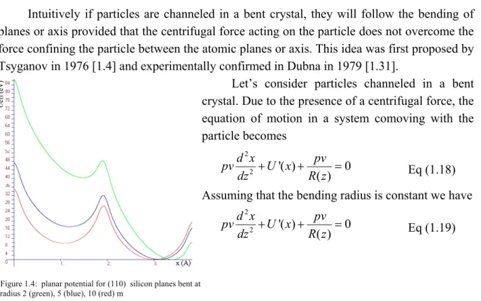
In Fig. [1.4] the Silicon (110) planar potential is plotted for different bending radius. Increasing the bending radius the depth of the potential well decreases, and its minimum becomes closer to the atomic planes. In correspondence of the “critical radius” [1.4],
2 '( ) c c p i pv pv R U x Nd Z Ze Eq (1.21) where U’(xc) is the interplanar electric field calculated at the critical approach distance xc, the well disappears and channeling is no more possible. Bending of the crystal lowers the depth of the potential well, decreasing the dechanneling length from the value ( )L Re Le( ) to
2
( ) ( )(1 / )
e e c
L R L R R , where ( )Le is the dechanneling length for a flat crystal
Particle deflection by axis is achieved by means of “hyperchanneling” and “doughnut-scattering” mechanisms. While in planar channeling a channeled particles travels between adjacent atomic planes, the majority of axially channeled particles are free to wander between
2 2 '( ) ( ) 0 d x pv pv U x dz R z Eq (1.18) 2 2 '( ) ( ) 0 d x pv pv U x dz R z Eq (1.19)
Figure 1.4: planar potential for (110) silicon planes bent at radius 2 (green), 5 (blue), 10 (red) m
doughnut-scattering mechanism provided that the “Shulga-Greenenko” condition [1.32-33] is satisfied, i.e. that
2 1 ( ) L k R Eq (1.22)
where L is the crystal thickness, R the bending radius and Ψ the axial critical angle. Assuming that such condition is fulfilled it is possible to achieve high efficiency deflection of the axial-channeled beam by means of both hyperchanneling and doughnut-scattering mechanism.
1.5. Volume Reflection (VR) and Volume Capture (VC)
Let us consider a bent crystal and a charged particle impinging on it. If the particle’s trajectory is aligned within the critical angle with crystal planes it is captured in channeling regime. Taratin [1.29, 34], by using computer simulations found that quasi-channeled particles, corresponding to such particles entering in the crystal at a distance smaller than the distance xr which defines the critical transverse energy for channeling, (see Fig [1.5]), are subject to Volume Capture (VC) or Volume Reflection (VR). Later, an analytical description of the VR process have been suggested by Maisheev [1.35]. Let us consider particles impinging on the crystal aligned with the crystal planes as in Fig [1.5] and at a distance with respect to the atomic planes less than the critical approach distance. A small fraction of particles, labeled as (1), are captured in channeling states (Volume Capture) due to dissipative processes which leads to a noticeable loss of transverse energy. The remaining fraction, labeled as (2), is subject to volume reflection, i.e. are deflected on the opposite side of the crystal bend. Deflection angle is comparable with the channeling critical angle.
Now let us consider the case that the crystal is aligned with respect to the particle beam in such a way that the particle trajectory becomes tangent to the crystal planes inside the bulk of the crystal, as in Fig. [1.6](b). Such particles will fall in quasi-channeling states inside the bulk of the crystal. Particles labeled as (1) are volume captured inside the volume of the crystal, while particles labeled as (2) are volume reflected of a quantity approximately 1.5 θc.
Figure 1.5: Changing of potential well shape and depth as function of crystal bending radius. xr is the interplanar region available for channeling
Figure 1.6 (a) particles subject to VR at the entrance on the crystal (b) particles subject to VR in the crystal bulk.
While VC has been used to increase the angular acceptance in channeling regime, and both experimentally [1.36-38] and theoretically [1.39-40] deeply studied in 1980 years, VR have been experimentally discovered only in recent experiments [1.41] and its features and peculiarities understood in experiments which will be described in this thesis. VC efficiency increases as decreasing beam energy [1.42]. Being VC antagonist to VR process the last one becomes highly efficient at high beam energy. For high energy particle beam manipulation VR offers big advantages with respect to channeling, providing a larger acceptance, (equal to the crystal bending radius) and efficiency close to 100%. In spite of this, the deflection angle is not so strongly dependant on crystal bending radius as it is for channeling and is comparable to the channeling critical angle.
Fig 1.7 summarizes interactions which can happen between a charged particle and a crystal. In Fig 1.7a-b straight crystal interacts with charged particles, which may see the crystal as an amorphous material or may be captured under channeling regime (only planar regime is shown for simplicity). In this case they will oscillate between the confining atomic planes with average period λ. If the crystal is bent as in Fig 1.7b-c and the particle trajectory becomes tangent to the crystalline planes inside the volume of the crystal it may be captured under channeling regime in the crystal bulk or it may undergo volume reflection.
Fig 1.7 Periodic planar potential in a straight crystal for positively charged particles. The arrows show a channeled particle with oscillatory motion in the potential depth and a nonchanneled particle, whose transverse energy is greater than the depth of the potential well Uo. (c) Schematic representation of the particle trajectories in a straight crystal. (b) Periodic planar potential in a bent crystal for positively charged particles. The arrows show volume-reflected, volume-captured, and channeled particles. (d) Schematic representation of the particle trajectories in a bent crystal.
In order to amplify the deflection angle it is possible to use a sequence of crystals properly disposed in such a way to multiply the deflection of each crystal (Multiple Volume Reflection from a sequence of crystals) or it is possible to use multiple volume reflection in one crystal (MVROC), which will be described in the following paragraph.
1.6. Multiple Volume Reflection in One Crystal (MVROC)
Under proper alignment between particle beam and crystal axis it is possible to excite VR from both crystal main plane and skew planes. This leads to multiple volume reflection in a single crystal, whose peculiarity is an increase of deflection angle and deflection efficiency about 90%. Let us consider a bent Silicon crystal with <111> axis and (110) channeling planes. Let the reference system xyz, oriented as in Fig. 1.7, be commoving with the impinging particle. Let us assume XYZ as a laboratory reference system. We consider the motion of the charged particle in the transversal xy plane. In laboratory frame the horizontal particle velocity is function of
the position in the crystal, we have infact vx=vx(z)=Vx-Vφ(z), φ(z)=z/R<<1. Differently, the vertical particle velocity is constant, Figure 1.7 Rapresentation of a particle incident on bent silicon crystal
close to <111> axis. XYZ is the laboratory reference system, while xyz is comoving with the particle and the z axis is always tangent to che crystal bent planes. Particle x component changes along the crystal, so the the vector (vx,vy) may become tangent to different planes
vy=Vy.
Due to changes in the horizontal component of velocity, under proper alignment between crystal and particle beam the particle transversal velocity (vx,vy) may become tangent to the skew planes, allowing VR from them. Reflection from skew planes will be characterized by deflection in both horizontal and vertical directions as Fig. 1.8 depicts. Deflection angles are given by θx=-θR*cosα and θy=-θR*cosα where α is the inclination angle of the plane, and θR is the deflection angle for a single VR from the given skew plane bent at radius R/sin(α). Since cos (π-α)=-cos α and sin α>0 for any 0< α< π, choosing the horizontal incidence angle such that θX0≈VX0/V=φ/2 horizontal deflections sum up, while vertical deflections from symmetrical skew planes cancels each other. In order to involve in the VR process the largest number of skew planes it necessary to minimize the angle θY0≈VY0/V. However such an angle should not be too small, otherwise particle will be subject to interaction with be volume captured by crystal axis instead of interacting with crystal planes. In order to exactly determine this angle it is necessary to realize simulations of the particle motion in the bent crystal, in any case a good criterion is to keep ΘY0 larger than about 4-5 times the axial critical angle.
To involve the reflection from a plane with inclination αpl a particle should impinge on the crystal at an angle α0=arctan(VY0/VX0)>αpl Due to this, the crystal bending angle has to satisfy the condition
0 0 0 0 0 0 0 2 X 2 X 2 cot 2 cot Y Y Y pl Y V V V V Eq (1.23)
For example, if we consider the skew planes (101) and (0 11) for which αpl=30° we have φ>3.46 . While for single volume reflection in a single crystal interaction is realized in the Y0 interaction with only the main plane, multiple volume reflection in a single crystal is due to interaction with many planes and involves alignment of the crystal in both horizontal and vertical directions. As a consequence the deflection angle depends on the vertical positioning of the crystal, which may allow or not interaction with some of the skew planes. In particular, deflection angle increases as the number of skew planes involved in the interaction with the Fig 1.8 a particle incident at angles Θx0, Θy0 is subsequently
reflected by skew planes and main plane. Vertical deflecions due to skew planes cancels each other, while deflections along horizontal directions sum up increasing deflection angle.
References
[1.1] Piercy G. R. et al., Phys. Rev. Lett. 10 399 (1963)
[1.2] Lindhard J., K. Dan. VVidensk. Selsk. Mat. Fys. Medd. 34 1 (1965)
[1.3] Feldman L. C. et al., Materials Analysis by Ion Channeling: Submicron Crystallography. 1982, Riverport Academic Press.
[1.4] Tsyganov E. N., Fermilab Preprint TM-682, TM-684 Batavia (1976) [1.5] Filatova N. A. et al., Phys. Rev. Lett. 48 488 (1982)
[1.6] Filatova N. A. et al., Nucl. Instr. and Meth. . 194 239 (1982)
[1.7] Carrigan R. A. and Ellison J., eds. Relativistic Channeling, pag 39. 1987, Plenum Press: New York.
[1.8] Andersen J. U. et al., Phys. Scr. 24 588 (1981)
[1.9] I. A. Grishaev G. D. K. a. B. I. S., Sov. Phys. JETP. 45 229 (1977) [1.10] Palazzi G. D., Rev. Mod. Phys. 40 611 (1968)
[1.11] Timm U., Fortschr. Phys. 17 765 (1969) [1.12] Carrigan R. A., Phys. Rev. Lett. 35 306 (1975) [1.13] Belkacem A. et al., Phys Rev. Lett. 54 2667 (1985) [1.14] Belkacem A. et al., Phys. Rev. Lett. 53 2671 (1984)
[1.15] Cue N. and Kimball J. C., Nucl. Instrum. Methods Phys. Res. B. 2 29 (1984) [1.16] Asseev A. et al., Phys. Rev. ST Accel. Beams. 1 22801 (1998)
[1.17] Murphy C. T. et al., Nucl.Instrum.Meth.B. 119 231 (1996) [1.18] Carrigan R. A. et al., Nucl. Instr. Meth. 90 128 (1994) [1.19] Afonin A. G. et al., Nucl. Instr. Meth. B. 234 14 (2005) [1.20] Afonin A. G. et al., Phys. Rev. Lett. 87 094802 (2001) [1.21] Baublis V. V. et al., Nucl. Instr. Meth. B. 90 150 (1994) [1.22] Chen D. et al., Phys. Rev. Lett. 69 3286 (1992)
[1.23] Khanzadeev A. V. et al., Nucl. Instr. Meth. B. 119 226 (1996) [1.24] Wang G. H. et al., Nucl. Instr. and Meth. 218 669 (1983) [1.25] Baker S. I. et al., Nucl. Instr. and Meth. B. 90 119 (1994) [1.26] Molière G., Z. Naturforsch A. 2 133 (1974)
[1.27] Leibfried C. L. G., J. Appl. Phys. 34 2821 (1963) [1.28] J.S.Forster, Nuclear Physics B 318(1989)
[1.29] Taratin A. M. and Scandale W., Nucl.Instr.Meth. B 262 (2007)
[1.30] Biryukov V. M. et al., Crystal Channeling and Its Application at High-Energy Accelerators. 1997 Berlin: Springer.
[1.31] Elishev A. A. et al., Phys . Lett. B. 88 387 (1979)
[1.32] Shulga N. F. and Greenenko A. A., Phys. Lett. B. 353 373 (1995) [1.33] Shulga N. F. and Greenenko A. A., Phys. Lett. B. 454 161 (1999)
[1.34] Taratin A. M. and Vorobiev S. A., Nucl. Instrum. Methods Phys. Res., Sect. B. 512 26 (1987)
[1.35] Maisheev V. A., Phys. Rev. ST Accel. Beams. 10 084701 (2007) [1.36] Andreev V. A. et al., Pis'ma Zh. Eksp. Teor. Fiz. 36 340 (1982) [1.37] Andreev V. A. et al., Pis'ma Zh. Eksp. Teor. Fiz. 39 340 (1984) [1.38] Andreev V. A. et al., Pis'ma Zh. Eksp. Teor. Fiz. 44 BII (1986) [1.39] Taratin A. M. and Vorobiev S. A., Zh. Theor. Fiz. 55 598 (1985) [1.40] Sumbaev D. I., Zh. Eksp. Theor. Fiz. 54 1352 (1968)
[1.41] Ivanov Y. M., Pis'ma Zh. Eksp. Teor. Fiz. 84 372 (2006) [1.42] Biryukov V., Phys. Lett. A. 205 340 (1995)
Chapter 2
Fabrication and bending of crystals for channeling
In a first generation of high-energy channelling experiments it was employed silicon crystals because of the availability of this material as single crystals of high crystalline quality. Such crystals were some centimetre thick along the beam, and bent through mechanical bending devices which were not able to impart a uniform bending radius [5.1-7]. Crystal bending exploited a primary bending imposed to the crystal. With the aim to realize shorter crystals and to provide uniform bending radius, two new generations of crystals were realized. Bending mechanism of such crystals relies either on “anticlastic deformation” (AD) use exploited by strip-like crystals [5.8] or on the “mosaic” (QM) effect exploited by quasi-mosaic crystals [5.9]. Both of them manifests as secondary curvatures due to a main imposed primary bending. Such curvatures are a multiple of the imposed main one, and for this reason are easily adjustable and allows realization of bending devices which can be placed far from the particle beam.
A second distinctive feature of the new generation of crystals is a higher quality of the crystal surfaces, i.e. of the surface over which the beam impinges and of the surface parallel to the particle beam. In the following we will describe as first the crystals preparation technique, and then their bending, focusing in particular to the strip-like crystals realized at the Sensors and Semiconductors Laboratory of Ferrara University.
2.1. Strip like crystals fabrication
Crystal fabrication requires dicing of the sample starting from either a wafer or an ingot to size the crystal to the wanted dimensions. This operation is normally accomplished by mechanical cut of base material. Such operation alters the original quality of the crystal, leading to the formation of a superficial “dead layer” with a great number of defects and crystalline disorder, which does not act as an active layer for channeling. Typically, preparation of suitably shaped crystals involves dicing of all crystal surfaces, both normal (entry face) and parallel to the beam direction. In order to realize crystals of the highest crystalline quality, we studied and optimized two methods based on wet isotropic and anisotropic chemical etchings. Such methods are borrowed from micro-fabrication techniques of silicon, were revisited and adapted to the case of sample preparation for channeling.
diffractometer (Philips MRD X-Pert PRO™) available at Physics Institute of Padova University. In particular, are selected crystals with miscut lower than 1 mrad.
2.1.1 Isotropic etching
A previous work [5.10] demonstrated that chemical etching was efficient for removal of the dead layer induced by mechanical dicing of the crystal surfaces. However, the process of etching resulted in significant roughness (Ra ~ 140 nm) of the surface in spite of its crystalline quality. Etching was conceived for application at the entry face of the crystal and thereby a relatively rough morphology was not a problem. On the strength of recently proposed usage of a crystal in modern hadron colliders and, in particular, of the constraint on the roughness of the lateral faces, an innovative methodology to treat the crystal’s surface was developed. Crystals were diced from a commercially available wafer using a “Disco DAD 3220” dicer, equipped with fine-grit blade to minimize the mechanical damage during the cut. In such machine is mounted a gentle diamond blade with average grains size of 1µm and thickness 150 µm rotating at the speed of 30.000 rpm. The wafer to be diced is mounted on a chuck and held in position by vacuum. The rotating blade accomplishes cutting operations positioning on the wafer with micrometer resolution. In order to remove the damaged region induced by the cutting process, we etched the whole crystal in
Figure 2.1 Removal of lattice damaged region induced by mechanical dicing. Region black in (a) rapresent damaged layer generated during crystal dicing. (b) The crystal is immersed in etchig solution, a layer of SiO2 (red) is created on all the crystal surfaces. SiO2 is removed by HF leaving a damage free crystal surfaces.
Figure 2.2 Schematic (not to scale) of the application of bent crystal for beam steering. The impact parameter b and the impinging angle of beam b are shown. The surface roughness Ra of the lateral face of the crystal (parallel to beam direction) is required to be lower than the impact parameter b (~ 100 nm for beam halo of LHC) for beam steering using the channelling effect.
an acid solution made of HF, HNO3, and CH3COOH (HNA) [5.11]. Such etching mixture is widely used in silicon micromachining.Nitric acid readily oxidizes Si to SiO2, which is eroded by HF, acetic acid serves as a solvent and makes the reaction more controllable. Such etching mixture is particularly suited to etch silicon isotropically, i.e. with the same rate independently of the crystallographic orientation. Silicon etching proceeds through the reaction
3 4 2
3Si12HF4HNO 3SiF 4NO8H O
Acetic acid is used as a diluent, it lowers in fact the etch rate of the reaction, making it more controllable. There is not much difference between the use of water or acetic acid, but
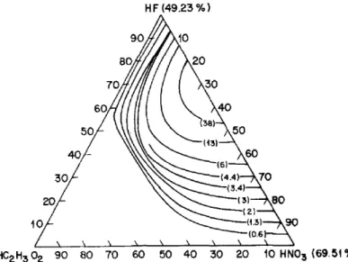
the last one is preferred because it results in less dissociation of the nitric acid, which preserves its oxidizing power over a wider range of dilution than water. From the tri-axial plot of Fig. 2.3 we gain the etch rate for any composition of the HNA etch solution. In the region of low HF concentration the etching process is diffusion-controlled, so different silicon materials are etched at the same rate. In the high HNO3 region the process is surface controlled, so we have a light dependence of the etch rate as function of crystallographic orientation.
Figure 2.3 Iso-etch curves for silicon etch in HF:HNO3 system, HC2H3O2 (acetic acid) is used as diluent
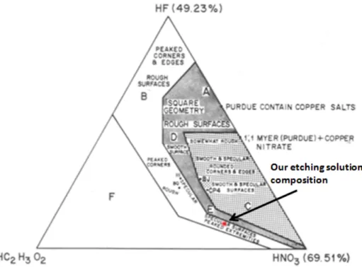
The morphology and geometry of etched surfaces is dependent of the relative etchants concentrations as showed in Fig. 2.4, where the red spot corresponds to HNA concentrations used in the etching solution employed for samples preparation. Assuming that lattice damage affect the diced crystal in the same way independently of the crystalline direction and with the aim to obtain a low roughness of the surfaces parallel to the beam we choose a composition of the etching mixture made of 2 parts of HF, 15 parts of HNO3 and 15 parts of acetic acid. This choice positions the HNA composition in a region of low HF concentration, and allows obtaining low roughness surfaces.
Figure 2.4 morphology of etched silicon crystals as function of HNA solution composition
After testing the solution on silicon wafers with different orientations we found that etch rate is 1 µm/min independently of crystal orientation. This confirmed that the etching solution isotropically etch silicon. The average size of the diamond grains contained in the dicing blade has size 1 µm, so it is reasonable that the lattice damage has an extension of the same order, so we choose and etching time of 2 min. The surface of the silicon crystals achieved through the procedure of dicing assisted by chemical etching was analysed from the standpoint of morphology and crystalline perfection, and compared to the surface just after the dicing process. Rutherford Back Scattering in Channelling condition (c-RBS) and Atomic Force Microscopy (AFM) were used for the purpose.
2.1.2. RBS and Channeling-RBS
Rutherford Backscattering (RBS) is a nuclear technique widely used to study composition of samples under analysis [5.12]. It is based on collisions between atomic nuclei and involves measuring the number and energy of ions in a beam which backscatter after colliding with atoms in the near-surface region of a sample at which the beam has been targeted. With this information, it is possible to determine atomic mass and elemental concentrations versus depth below the surface. In the case the target material is crystal, orienting it in channeling alignment (Channeling- RBS) it is possible to determine the crystalline quality. When a sample is bombarded with a beam of low energy particles, the vast majority of particles are implanted into the material and do not escape. Energy exchange occurs because of Coulombic forces between nuclei in close proximity to each other. However, the interaction can be modeled accurately as an elastic collision using classical physics. The energy measured for a particle backscattering at a given angle depends upon two processes. Particles lose energy while they pass through the sample, both before and after a
collision. The amount of energy loss is dependent on that material's stopping power. A particle will also loose energy as the result of the collision itself. The collisional lost depends on the masses of the projectile and of the target atoms. The number of backscattering events that occur from a given element in a sample depend upon two factors: the concentration of the element and the effective size of its nucleus. For scattering at the sample surface the only energy loss mechanism is momentum transfer to the target atom. The ratio of the projectile energy after a collision to the projectile energy before a collision is defined as the kinematic factor. 2 2 1 1 2 2 1 2 sin cos 1 1 scattered incidend M M M M E K M E M (2.1)
Where E is ion energy, M1 and M2 are mass of incident ion and mass of target atom and θ is the scattering angle. From this relation it’s clear that it is convenient to use light atoms as probes. The relative number of particles backscattered from a target atom into a given solid angle for a given number of incident particles is related to the differential scattering cross section. The scattering cross section is basically proportional to the square of the atomic number of the target atom. Only a small fraction of the incident particles undergoes a
close encounter with an atomic nucleus and are backscattered out of the sample. The vast majority of the incident ions end up implanted in the sample. When probing, particles penetrate to some depth in a dense medium, projectile energy dissipates due to interactions with electrons (electronic stopping) and to glancing collisions with the nuclei of target atoms (nuclear stopping). This means that a particle which backscatters from an element at some depth in a sample will have measurably less energy than a particle which backscatters from the same element on the sample surface. The amount of energy a projectile loses per distance traversed in a sample depends on the projectile, its velocity, the elements in the sample, and Figure 2.5 Relative yields for He backscattering from selected
elements at an incident He energy of 2 MeV. The energies for He backscattering from these elements when present at the surface of a sample are also displayed. RBS is over 100 times more sensitive for heavy elements than for light elements, due to the larger scattering cross sections of the heavier elements.
2.1.3. RBS-Channeling
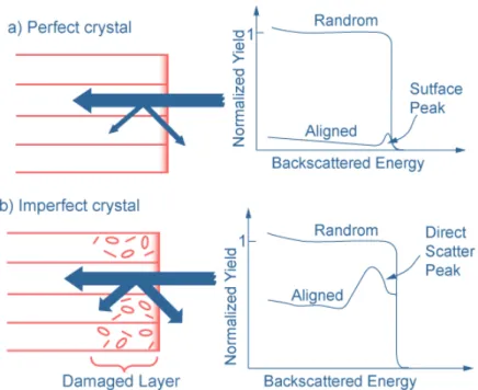
In addition to elemental compositional information, RBS can also be used to study the structure of single crystal samples. When a particle is channeled, the rows of atoms in the lattice are aligned parallel to the incident ion beam. The bombarding ion will backscatter from the first few monolayers of material at the same rate as a non-aligned sample, giving a “surface peak” in the RBS-Channeling spectra, but backscattering from buried atoms in the lattice will be drastically reduced since these atoms are shielded from the incident ions by the atoms in the surface layers. For example, the back- scattering signal from a single crystal Si sample which is in channeling alignment along the <100> axis will be approximately 3% of the backscattering signal from a non-aligned crystal, or amorphous or poly-crystalline Si. By measuring the reduction in backscattering when a sample is in channeling, it is possible to quantitatively measure and profile the crystal perfection, and to determine crystal orientation. As depicted in Fig. 2.6 (a) for a perfect crystal yield for channeling orientation is much lower than for random orientation. For a not perfect crystal yield is higher than amorphous case but lower than for a perfect crystal. On diced and chemically treated samples C-RBS was carried out with 2.0 MeV 4He+ and 1H+ beams in IBM geometry, depicted in Fig 2.7.
Figure 2.7 scheme of IBM geometry used in C-RBS analysis. α is the incident angle, β the exit angle and θ the scattering angle. In our case θ=160°
Figure 2.6 Channeling RBS working principle. (a) schematic RBS spectra for a perfect single crystal. In channeling alignment it is observed a strong reduction of the yield. (b)
As quantifier of the crystalline quality we use the quantity χmin, defined as the ratio of the RBS yield under channelling alignment and random condition measured at the surface. The higher the degree of crystalline order in the lattice the lower the surface χmin due to the reduction of dechanneling from the defects in the crystal. The quality of the surface was correlated with preparation methodology for direct comparison with previously reported results [5.10] and the stringent condition for halo cleaning in hadron machines. The C-RBS spectrum of etched sample in random and aligned condition is reported in Fig. 2.8 for 4He+ (a) and 1H+ (b) beams.
Figure 2.8 C-RBS spectra on silicon crystal oriented along the [110] direction, after chemical etching, using (a) particles and (b) protons, E0=2.0 MeV, IBM geometry, scattering angle =160°. The dashed spectra refer to random orientation of the crystal. The investigation was carried out down to about 1.5 m and 10 m deep into the crystal for particles and protons, respectively. For both alpha particles and protons the surface min (2.2% and 2%, respectively) is close to the semiempirical value for a perfect crystal (see Ref. [5.13]).
Analyzed region extends over 1.5 and 10 µm, respectively. The pronounced surface peak in the α particle spectrum is due to the random scattering from the first atomic layers, before that the crystal potential starts to focus the beam at the centre of the channels. The peak
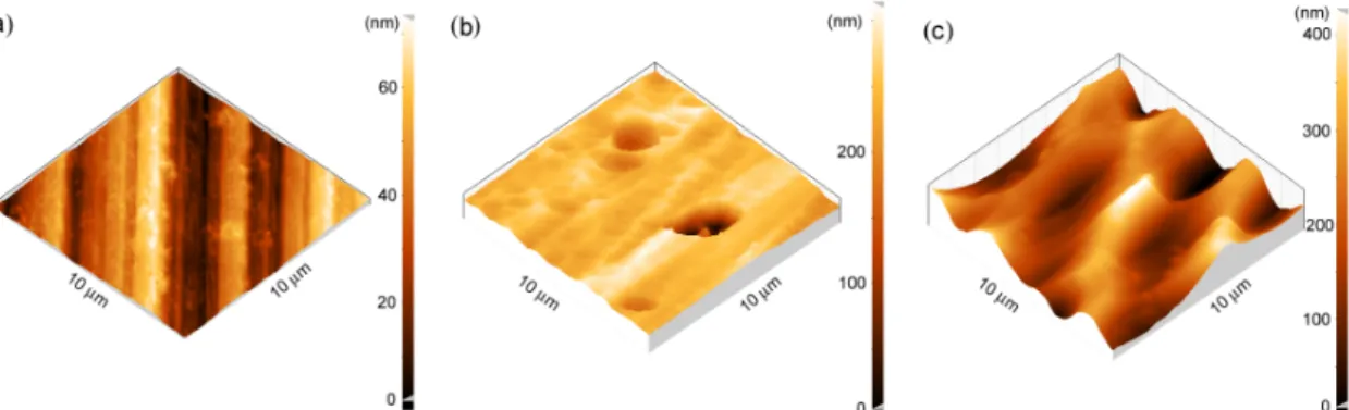
The standard surface roughness, Ra, was measured by means of Atomic Force Microscopy (AFM). Figure 2.9 collects AFM images of the (110) surface just after cut (a), after the chemical etching described in this work (b), and after the etching imparted according to Ref. [5.10](c). The scrapes due to the effect of the blade on silicon surface are normal to the direction of the cut, which are barely visible after etching. Quantitative results are reported in Tab. I.
Figure 2.9 AFM pictures of the silicon crystal: (a) just as-cut; (b) after etching according to the procedure here described (c) after chemical etching according to the procedure in Ref. [5.10]. The scrapes due to the blade are visible in the as-cut sample, while they are nearly completely removed after chemical etching. The procedure of etching here described, based on fast and homogeneous oxidation of silicon and subsequent erosion of silicon oxide, allows removal of the surface "dead layer" without formation of undesired craters worsening the surface flatness. Ra is more than 5 times lower with respect to the preparation methodology
according to Ref. [5.10].
Table I Standard roughness Ra and surface χmin (using α particles) of silicon crystals just after cut and after chemical etching. Ra is defined as follows:R 1 z i j( , ) z
a n m i j where z(i,j) is a height record of an nm image and z is the
height average. Results are based on AFM and c-RBS analysis, respectively, and are compared with numerical data
from Ref. [5.10].
Ra (nm) χmin
Sample Ref. [5.10] This work Ref. [5.10] This work
As cut 15±5 15±5 (16±1)% (16±1)%
Etching 135±10 23±5 (4.1±0.2)% (2.2±0.2)%
Chemical etching highly removed lattice defects from the surface as highlighted by the surface χmin=2.2% for α particles, which equals the semiempirical values for a perfect silicon crystal along the [110] axial direction (χmin~2%, see Ref.[5.13, 14]]), and improves previously achieved result [5.10] (surface χmin=4.1%). For protons, surface χmin gives about 2% a value in agreement with the semiempirical value also in this case. Table I summarises the results of AFM and c-RBS and gives quantitative comparison with numerical data of Ref. [5.10]. In short, the two main benefits can be envisaged in the chemical etching described in this work: firstly, it improves the effectiveness in removal of the surface damaged layer, providing better crystal quality. Secondly, it yields a very smooth surface (below 25 nm) as compared with previous results, and consistent with the requirement for beam collimation.
2.2. Anisotropic etching
With the aim to realize strip crystals without inducing any lattice damage during their fabrication we developed a fabrication technique based on silicon anistrotropic etching This mode allows to engrave a silicon crystal and, differently from the isotropic etching allows to realize complex structures in silicon, among them also multi-strip crystals, which will be described later.
In contrast to previously used isotropic etchings, there is class of chemical reactions based on alkaline solutions whose erosion rate depends on the crystalline orientation. In particular, planes (110) show the highest etch rate, (111) planes are the most resistant and (100) are in between. Indeed, anisotropic etching is a widely employed technique in modern micro-machining of Si [5.15]. Thus, with proper choice of the components of the solution, anisotropic erosion would results in a high-precision cut of a crystal (see Fig.2.10). A widely used silicon anisotropic etchant is Potassium Hydroxide (KOH). With the identification of H2O and OH- as reactant the overall reaction is
2
2 2 2 2
2 2 2 ( )
Si H O OH H SiO OH
Empirically [5.16] it have been found that for KOH solutions with concentrations in the range 10-60% the silicon etch rate is given by the relation
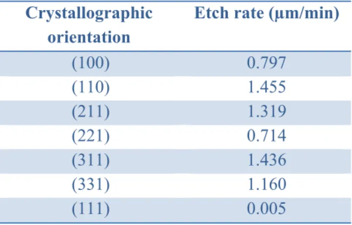
Where k0=4500 µm/h*(mol/L)-4.25, Ea=0.60 eV for (110) planes, k0=2480 µm/h*(mol/L)-4.25 and Ea=0.595 eV for (100) planes. Table II summarizes etch rate for different planes of Silicon.
/ 4 1/ 4 0[ 2 ] [ ] a
E KT
R k H O KOH e (2.2)
Figure 2.10 Schematic view of fabrication of a silicon crystal via anisotropic etching. (a) sample after patterning with Si3N4 (dark regions) and prior to chemical attack; (b) the unmasked areas undergo etching along the <110> direction while negligible erosion occurs along the <111> direction. Proper timing allows one to make controlled indentations or complete cut of the sample
Table II Etch rate for different silicon planes in 30% KOH at 70°C. (110) planes are etching much faster (111) planes.
Crystallographic orientation
Etch rate (µm/min)
(100) 0.797 (110) 1.455 (211) 1.319 (221) 0.714 (311) 1.436 (331) 1.160 (111) 0.005
Exploiting anisotropic behavior of silicon in KOH solutions Si crystals were prepared. Starting material are 4-inches (110) Si wafers with the wafer’s flat oriented perpendicular to <111> direction. A 100 nm layer of Si3N4 was deposited onto all faces of the wafer through low-pressure chemical vapor deposition and patterned with standard photolithographic techniques [5.17] with the masking pattern aligned with the wafer’s flat. The wafer was immersed in KOH solution (40% weight concentration) with the Si3N4 pattern as a masking layer [5.18] and kept at 70°C until the holes where completed, which resulted in erosion of uncovered regions on the wafer.
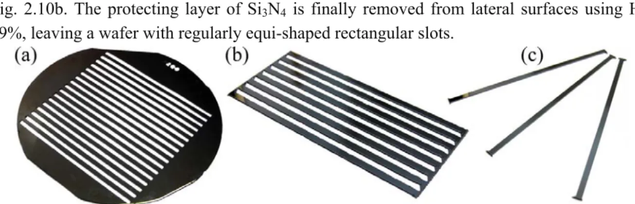
For the experimental parameters of the solution we chose, the etch rate of (111) planes is negligible with respect to the (110) planes so that chemical erosion proceeds as depicted in Figure 2.11 Fabrication of crystals for channeling (not to a scale) (a) deposition of a uniform 100-nm thick Si3N4 layer, (b) pattering of Si3N4, (c) anisotropic KOH etching and mechanical dicing along either the dashed line to release a series of independent strip-like crystals or the solid line to manufacture a multi-strip crystal with a frame, (d, e) final removal of the Si3N4 film. Masking by KOH resistant Si3N4 thin film patterned onto the surfaces of the Si crystal allows fabrication of rather complex geometries.
Fig. 2.10b. The protecting layer of Si3N4 is finally removed from lateral surfaces using HF 49%, leaving a wafer with regularly equi-shaped rectangular slots.
Figure 2.12 From left to right: a 4’’ silicon wafer with full passing holes realized by anisotropic etching. A silicon multistrip and silicon strips obtained by mechanical dicing of the wafer
Then, the wafer can be cut in such a way to achieve either a batch of independent strips (Fig.2.12c) or a rigid frame interconnecting a series of regularly positioned strips (Fig.2.12b). In the case of strip-shaped crystals, they were sized as (0.5-2)(0.3-0.5)70 mm3 because these
dimensions best matched the requirements for application in the CERN SPS external lines H8 and H4, the first operating with 400 GeV protons, the second with 120-150 GeV negative particles. The other geometry was studied to excite multiple volume reflection as a result of deflection of the particles with each strip [5.19]. Spacing and thickness of multi-strip crystals varies in the range 0.5 to 2 mm. More generally, the pattern of the photolithographic mask enables the achievement of a strip with any size of more complex structures that can be achieved by dicing the wafer parallel or perpendicularly to the lattice directions. Morphological investigation of the roughness of the crystal surface was done by atomic-force microscopy (AFM). Analysis was carried out over one of the (110) surfaces of the samples, i.e., to the lateral surface of the crystal, which are the planes first interacting with halo-beam
particles. Clear evidence of ultra-flat surface with a roughness down to the monolayer level was achieved over a relatively wide scan (1010 µm2). Standard roughness is a quantifier of the flatness of a surface, which is defined as
R
a
1
n
m
jz(i, j)
z
m
i n
,where z(i,j) is the height record of an nm image and z is the height average. Standard
roughness featured Ra=0.25 nm, i.e., Ra was decreased by nearly two orders of magnitude
Figure 2.13 AFM image taken over a 1010 µm2 area on the lateral surface of the crystal. Standard roughness keeps down to the sub-nanometric level for the sample under study.
Figure 2.14 SEM images of the crystal, a) tilted view of the flat crystal upper surface and of the smooth <111>-oriented entry face, which is marked by an arrow. b) magnified view at normal incidence of the <111> entry face, showing very uniform morphology.
The sample was analyzed by scanning and transmission electron microscopy (SEM and TEM). Fig 2.14a shows a panoramic view of the sample. The SEM image highlights the homogeneity of the upper (110) surface of the sample and the uniformity of the (111)-oriented side face. This latter features some vertical steps, due some alignment mismatch between the mask and the <111> direction. At higher magnification, the SEM image of Fig. 2.14b shows that the surface of the entry face is very smooth and homogeneous.
For TEM characterization of the entry surface of the crystal and the sub-surface region, a cross-section specimen was prepared through a conventional process of mechanical polishing and ion milling. The TEM bright-field image shown in Fig. 2.15a highlights a straight termination of the crystal surface, and the contrast variations indicate that the preparation resulted in a smooth edge-shaped sample with no evidence of mechanical damage introduced by the thinning procedure. No lattice defect was observed in the sub-surface region of the sample. Indeed, the ripples in the bright-dark contrast fringes of the TEM bright-field image arise from a gradual increase of the projected thickness of the wedge-thinned specimen. Presence of extended defects in the Si lattice, such as dislocations, is ruled out. Such defects would have introduced local distortions in atomic positions and therefore the variation of intensity for the diffracted electron beam would have resulted in abrupt variation of the image contrast. The observation at high resolution (see Fig. 2.15b) shows an ordered arrangement of atomic columns, which is preserved up to the crystal surface, i.e., the crystal is terminated with atomically sharp ordering. The electron diffraction pattern of Fig. 2.15c confirms that the exit direction of the beam is parallel to the <111> crystal direction. Similar observations over different area of the sample confirmed previous determinations.
Figure 2.15 TEM characterization of the entry face of the crystal. a) low-magnification panoramic view of the entry face as visible in the cross-sectioned specimen. The white-black contrast fringes are due to smooth variation of sample thickness. b) High-resolution image of the ordered and atomically sharp termination of the crystal surface. The amorphous material above the crystal is the embedding epoxy used in the preparation of the cross-section sample. c) Electron diffraction pattern of the sample, indicating that the surface is parallel to the <110> direction.
2.3. Crystal bending
Elastic strips or tapes (wires) are commonly used in industrial applications. When such strips are bent, the longitudinal strains, which are purposely induced, are accompanied by lateral strains in the width direction of the strip. As a result, the strip takes the shape of a saddle, i.e., it bends to a surface in which the two principal curvatures are opposite in sign. This effect is referred to as anticlastic deformation (AD). For an amorphous material, if the longitudinal radius of curvature, i.e., the primary radius of curvature, R, into which the strip is being bent is large, the cross section is found to deform to an arc of a circle with secondary radius RA = R/v, where v is Poisson’s ratio [5.20]. Thus, although the extent of AD is not large, it may cause practical difficulties. As an example, the edges of the magnetic tapes used in computer applications are found to wear because of it. Similar difficulties are encountered in the bending of the long metallic plates used to form the adjustable working sections of wind tunnels. The consequent AD of the plates is found to interfere with the air flow. Although possible remedies to counteract anticlastic deformation do exist, e.g. by proper tapering of the edges on the concave sides of the tapes or plates, there are applications in which AD is desirable. A significant example is particle-beam steering through channeling in a crystal. As one might expect, AD of an anisotropic material, as needed for channeling experiments, would lead to significant dependence of the curvature ratio R/RA on the chosen crystallographic direction.
2.3.1. Anticlastic deformation in an anisotropic material
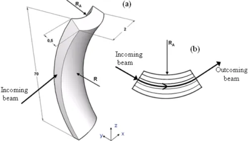
We herewith review some concepts of anticlastic deformation in a isotropic material that are necessary for understanding further modelling. A typical strip crystals is 70x2x0.5 mm3 wide (see Fig. 2.16). Thereby, the shape of the crystal is such that the theory of a mechanical beam can be worked out extensively.
Figure 2.16a Sketch of a bent silicon strip for channeling experiments. Anticlastic deformation with radius RA arises as a result of primary bending with radius R. Quotes are expressed in mm and represent typical values for high-energy experiments. (b) Cross-section of the crystal; the incoming particles are captured by the potential of atomic planes and the beam is being deflected.
Crystalline silicon exhibits FCC cubic symmetry and diamond lattice with each atom on the centre of a tetrahedron with four nearest-neighbour atoms at the four vertexes. Thereby, Young’s modulus and Poisson’s ratio are direction dependent [5.21]. As for any FCC symmetry, the elastic properties are completely characterized by only 3 independent constants. For Si, the compliance matrix, S, referred to the canonical base <e> = <100>, <010>, <001>, (where <100>, <010>, <001> are main crystalline axes of the cubic cell), takes the form:
7.678 -2.144 -2.144 0 0 0 7.678 -2.144 0 0 0 7.678 0 0 0 12.531 0 0 12.531 0 12.531 e Sym S x10-3MPa (2.3)
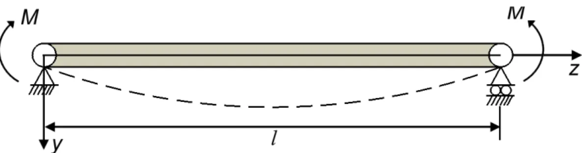
In channelling experiments, the crystal is bent to a relatively modest curvature and the primary deformation is imparted at the edges of the strip through a mechanical couple of moment M by clamping onto a rigid holder which will be described later. Such a system can be modelled as a homogeneous and anisotropic bar under infinitesimal deformations and
small displacement, supported at its ends by kinematics and concentrated supports and bent by a point-like couple of forces at its edges, as shown in Fig. 2.17.
Figure 2.17a Schematic representation of bending of a beam of length l under the action of a couple of moments applied at its ends.
The displacement of the strip along y direction is given by [5.22]
2 2 2
13 23 33 35 33 1 ( , , ) = + + ( ) 2 v x y z a x a y a lz z a xz a R (2.4)where aij are the 6x6 coefficients of S<e> . Presence of the z2 term is related to the imposed principal bending while the x2 term shows that x-y cross section is deformed as a parabola, giving rise to anticlastic bending, whose magnitude is linearly proportional to the imposed bending. The mostly direct observable physical quantity is the principal curvature while anticlastic deformation is quantified by the secondary curvature. Thus, the ratio RA/R determines the extent of anticlastic deformation in dimensionless units. Differently from the case of an isotropic material, the ratio between anticlastic and principal bendings is determined by the two components of the elastic compliance tensor. For our applications, the region of interest is the central part of the crystal so that RA/R is calculated at x=0, y=0, z=l/2:
33 13 = A a R R a (2.5)
It should be remarked that a33 cannot vanish; thereby it is impossible to find a bent silicon crystal without anticlastic deformation. Moreover, R and RA have opposite signs, i.e., the crystal takes the shape of a saddle. It should be remarked that Eq. (3) holds for crystals narrow enough in the width direction such to develop a plain stress regime. In fact, by increasing the crystal width, b, the system tends to behave like a plate under plain strain condition, thus preventing anticlastic deformation [5.23]. As reported in [5.23-25], an estimator of this behaviour is the “Searle parameter”,
where t is crystal thickness. If β<1, anticlastic bending arises on the whole crystal width (beam-like behaviour). Conversely, if β>>1, anticlastic bending is remains only in the external regions of the crystal (plate like behaviour). As will be demonstrated in the following, we will always deal with the case β<<1. The ratio in Eq. (2.5) is orientation dependent so that designing a bent crystal for channeling and volume reflection experiments demands its knowledge for any orientation of the strip. For planar channeling and volume reflection, the (110) planes were found to be best efficient, namely the crystal is to be oriented with such axis along y axis in Fig. 2.17. The remaining two directions are to be chosen and R/RA should be studied as a function of the base, <m>, with the vectors parallel to the sides of the crystal.
Thereby, the compliance tensor in the base <m> is linked to S<e> through a similarity transformation:
T
<m> <e>
S KS K (2.7)
K being the rotation matrix connecting the <e> base to the <m> base.
2.3.2. Simulation and experimental
In order to study the orientation dependence of strained silicon strips, several crystals of size 2x0.5x70 mm3 were diced from a 0.5 mm thick (110) silicon wafer, and the induced lattice damage was removed by isotropic etching previously described. The wafer’s “flat”, i.e., the cut done by the manufacturer for better usage of the wafer was parallel to the (1 10) plane. The crystals were cut at some inclination, θ, with respect to the flat (see Fig.3 and Tab. I) and all of them were oriented with the
<110> direction along y axis. The ratio RA/R was studied by bending the crystal through the holder typically used in channeling experiments and which will be described later.
Figure 2.18 Silicon crystals are diced from a (110) wafer. The length of 70 mm is achieved at several angles with respect to the wafer’s flat. The Y axis is always the <110> direction, while x and z vary as function of θ
Table III Ratio between anticlastic and principal bending radii as a function of : comparison between theoretical model, measurements and FEM simulations.
θ(deg) RA/R(measured) RA/R (theoretical) RA/R(FEM) 0 -3.52 -3.59 -3.58 15 -3.98 -4.00 -4.00 35.26 -6.31 -6.20 -6.15 45 -6.82 -6.80 -6.73 60 -4.72 -4.70 -4.67 75 -3.16 -3.15 -3.14 90 -2.75 -2.76 -2.75
The principal and anticlastic radii were measured by means of a white-light profilometer (Veeco NT1100) capable of recording the profiles of the bent crystal with height resolution of 3 nm. In order to make the surface orientation independent of the alignment with respect to the profilometer objective, tilt and piston terms were removed via software.
Fig. 2.19 shows a typical profile of the strip taken in a central region 2x2 mm2 wide, which exhibits a saddle-like surface as predicted by elasticity theory.
Figure 2.19 Deformation of the crystal surface when bent by the holder. The crystal is diced at =35.26°. A saddle deformation is visible thanks to interference fringes.
Fig. 2.20 illustrates the experimentally recorded levels of RA/R for the values of in Tab. I. Clear signature of orientation dependence is observed with the ratio RA/R attaining its maximum for the direction <1/√2 1/√2 1> and its minimum for the direction <100>. Such
Figure 2.20 Ratio |RA/R| as function of θ (for its definition see Fig. 2.18). Experimental data are compared with FEM simulation and with the model. The figure shows that the ratio |RA/R| is direction dependent as expected from a crystal.
The expected ratio of |RA/R| versus the angle θ, reported in Fig. 2.20, has been obtained analytically by calculating the ratio |a33/a13|, which is the Poisson ratio for the corresponding crystalline direction, according to classical mechanical beam theory. Fig. 2.20 also includes experimental results for the ratio |RA/R|, which are in good agreement to theoretical values for each crystalline direction.
It should be remarked that Eq. (2.4) holds true for the ideal case of concentrated supports at the edges of the strip but, in practice, clamping of the crystal mounted on the holder occurs over a finite region. Thereby, distortion of the shape of the bent crystal from a saddle is expected, particularly in proximity of the holder jaws. To our knowledge, an analytical formulation including a non point-like constrain does not exist in literature. With the purpose to take into account information about the portion of crystal not influenced by the presence of holder jaws, Finite Element Method (FEM) simulations based on STRAUS7 software (release 2.3.3) have been worked out considering the geometry of the holder used in this work (see Fig. 4), which is routinely used in channeling experiment. Furthermore, according to the works in Ref. [5.24, 25] aimed to a more homogeneous bending, we also considered the possibility to realize new clamping conditions to hold the crystal. A sketch of the FEM mesh is given in Fig. 2.20. Since the deformation of the crystal is expected to be not appreciably affected by the whole holder structure, only the jaws of the holder have been modelled in our numerical simulation. The silicon crystal was modelled as 3D anisotropic cubic bricks elements, whereas the aluminium supports of the holder were modelled as isotropic 3D elements.
Figure 2.21 Mesh of a Si strip mounted on the holder jaws for FEM. The strip (2x0.5x70 mm3) is simulated by 528-brick elements, whereas 36496 bricks elements model the holder supports.
Both the strip and the holder were considered homogeneous elastic bodies under small strains. The strip was assumed to be perfectly bonded to the holder supports. Bending of the silicon strip is achieved by imposing rotations of both the lower aluminium jaws along the x axis, obtaining a symmetric flexure of the crystal in the yz plane. Fig. 2.22a shows the dependence of |RA/R| as a function of coordinate z for the first half of the strip bent at R = 1.5 m for some crystalline orientations.
Figure 2.22 FEM-simulated values of |RA/R| along the length of a (2x0.5x70 mm3) bent crystal for some crystalline orientations and R = 1.5 m The numerical values agree with the theoretical prediction based on Eq.(3) except for a small region of the crystals close to the holder jaws.
The same results are shown in Fig. 22b expressed as normalized ratio at the beginning 0 0,2 0,4 0,6 0,8 1 1,2 b) 75 0 15 35.26 45 60 90 l/2 l/4 3l/8 l/8 0 z coordinate |R A /R |/ |R A /R |z= angle 0 5 10 15 20 25 30 35 40 75 0 15 35.26 45 60 90 a) l/2 l/4 3l/8 l/8 0 z coordinate |R A /R angle