M
arta Antonella Agati
600 700 800 900 1000 P L ( ar b. u nit s) Wavelength (nm)Università degli Studi di Catania
Dipartimento di Fisica e Astronomia
Dottorato di Ricerca in Fisica XXIX Ciclo
Transmission Electron Microscopy studies of
the nanostructural characteristics of the
Inductively Coupled Plasma synthesized
Silicon Nanowires
Tesi per il conseguimento del titolo
Marta Antonella Agati
Supervisors: Dr. S. Boninelli (CNR-IMM, Italy)
Prof. M. A. El Khakani (INRS-EMT, Canada)
Prof. G. Angilella (Università di Catania, Italy)
Coordinatore: Prof. V. Bellini (Università di Catania, Italy)
iii
Imagination is more important than knowledge. For
knowledge is limited to all we now know and understand,
while imagination embraces the entire world, and all there
ever will be to know and understand.
iv
Cover
From the left to the right:
Energy Filtered Transmission Electron Microscopy image
depicting core/shell Silicon/Silicon Oxide Nanowires grown
via oxide-assisted-growth mechanism.
Representative image of the inductively coupled plasma based
reactor.
Energy Filtered Transmission Electron Microscopy image of a
Silicon Nanowire grown via vapor-liquid-solid
mechanism.
Typical room temperature photoluminescence spectrum of the
Silicon nanowires.
iii
Table of Contents
1. Relevance of low dimensional Silicon for nanotechnology ... 1
1.1. Market trend in the Si-based nanotechnology... 1
1.2. Quantum confinement effects in Si nanostructures ... 5
1.2.a Bandgap engineering ... 7
1.2.b Correlation between theoretical models and experimental results ... 10
1.3. Context and objectives of the PhD Thesis ... 14
Bibliography ... 16
2. Growth mechanisms of Si nanowires and their associated synthesis techniques ... 19
2.1. Growth Mechanisms for SiNW formation ... 19
2.1.a Vapor-Liquid-Solid mechanism ... 20
2.1.b Oxide Assisted Growth mechanism ... 26
2.2. Conventional techniques for SiNW synthesis ... 32
2.2.a Chemical Vapor Deposition ... 33
2.2.b Molecular Beam Epitaxy ... 35
2.2.c Laser ablation ... 36
2.2.d Thermal evaporation ... 38
2.3. Conclusions ... 39
Bibliography ... 40
3. Experimental details ... 45
3.1. Inductively Coupled Plasma for large scale production ... 46
3.1.a Micropowder synthesis ... 47
iv
3.2. Transmission Electron Microscopy ... 51
3.2.b Electron tomography ... 64
3.3. Photoluminescence spectroscopy ... 66
3.4. Conclusions ... 68
Bibliography ... 69
4. Investigation of SiNWs synthesised by ICP ... 73
4.1. Structural and chemical characterization ... 74
4.2. Growth mechanisms of ICP-produced SiNWs ... 80
4.2.a SiNWs produced by Oxide Assisted Growth mechanism 80 4.2.b SiNWs produced by Vapor Liquid Solid mechanism ... 84
4.2.c 3D reconstruction of VLS SiNWs by Scanning Trasmission Electron Tomography ... 87
4.2.e Surface diffusion above the Fe catalyst ... 91
4.3. Quantum confinement effect in ICP-SiNWs ... 92
4.4. Conclusions ... 96
Bibliography ... 96
5. Sorting protocol to extract SiNWs ... 99
5.1. Purification process performed by centrifugation ... 100
5.2. Photoluminescence tuning by size selection ... 103
5.3. Evaluation of the purification efficacy by SEM ... 105
5.4. Conclusions ... 108
Bibliography ... 108
6. Thermal treatment to form Si nanocomposites via Rayleigh instability 109 6.1. Study of the thermal stability of SiNWs ... 110
v
6.1.b Ex-situ analyses ... 113
6.2. Rayleigh instability ... 117
6.3. Conclusions ... 119
Bibliography ... 120
7. Conclusions and perspectives ... 121
7.1. Conclusions ... 121
7.2. Perspectives: exploitation of a novel ICP process ... 123
8. Publications ... 129
9. Conferences and Schools ... 131
Conferences ... 131
Schools ... 132
1
1. Relevance of low dimensional
Silicon for nanotechnology
1.1. Market trend in the Si-based
nanotechnology
After several decades of scientific research, the ongoing implementation of nanotechnology into the global market signs a crucial step in the research & development of new and highly performing nanomaterials, and this new trend has often been described as a novel industrial revolution. As an estimation of the assimilation of nanotechnology into the every-day life, the number of products incorporating nanomaterials has been evaluated to grow from 54 in 2005 to 1200 in 2015, with an average annual growth rate of ~110% (Fig. 1). A recent report states that the annual global market for nanotechnology based goods will reach US $3.3 trillion by 2018 [GlobalInfoInc14]. Moreover, the Compound Annual Growth Rate in nanotechnology market has been expected to reach the ~17.5% during the 2016-2022 period [MarketOutlook15].
In this framework, silicon (Si) has been defined the cornerstone for the development of microelectronics in the past few decades. In 1947 Walter Brattain and John Bardeen, members of Solid State Physics Group headed by William B. Shockley, created the first transistor prototype, marking the beginning of the new era based on computer technology. For several decades, since its initial development, the performances of microelectronics
2
devices were intuitively predicted by Moore, one of the founders of the Intel Corporation. Indeed, in the 1960s, he predicted that the number of transistors in an integrated chip would double every two years, implying the exponential increment of chips' power as well as the scaling down of Si-based devices [Moore65]. Device’s miniaturization predicted by Moore's law inspired for decades the philosophy of the Silicon Valley and has been the bedrock for the computer companies as well as for the pioneers of computer science.
Fig. 1. Number of products in the nanotechnology market containing nanomaterials.
σevertheless, in the 1λλ0s an inflection point in Moore’s law (see Fig. 2) has been remarked and nowadays it seems that this trend is not still valid because of the occurrence of serious obstacles which technology has to be faced with. The main limitations are related to: (i) lowered device
performances (short channel effect becomes more important in miniaturized
devices), (ii) more complex fabrication processes (extreme miniaturization causes an increase of production costs since more complex lithography and etching systems are required), (iii) system performances (related to interconnection length that becomes longer and longer, introducing increasing delay in the transmitted signals) [Xu12]. Nonetheless, at the
3 beginning of this century innovative different approaches have been considered to overcome these limitations. The strategy developed within the so-called “More than Moore” approach consists into envisaging new functionalities of electronic devices that do not necessarily scale according to Moore's Law [ENIAC07]. This approach refers to a set of technologies enabling not necessarily digital micro- or nano-electronic functions; indeed, this trend tries to convert non-digital and non-electronic data, such as mechanical, thermal, acoustic, chemical, optical and biomedical functions, into digital ones and vice versa.
Fig. 2.Illustration of Moore’s lawμ the dashed line shows the doubling of transistors in a chip
every two years. We can see that between 1λλ0 and 2000 Moore’s law had an inflection point. In general, Moore’s trend is forecasted to slow down in the next years [webinfo].
In this contest, most likely Si will remain the material of choice for a wide range of applications in the future. Indeed, its natural abundance and its
non-4
toxic nature contribute to preserve the role of Si as the material of choice to design future-generation applications. In addition, the existence of the well-established infrastructures and technologies of Si-based microelectronics, which bears a significant know-how on the material as well as the whole apparatus of processes and facilities, will favor the employ of Si for future applications. The most important contribute in the recent years has been given by the use of Si in solar panels, predominantly via the fabrication of polycrystalline Si-solar cells. Indeed, 90% of solar panels customized nowadays is made of Si-based materials [Priolo14]. Si-based photovoltaics has also reached a record in terms of the maximum attainable performance for single junction solar cells, for which it has been reported an efficiency of 25% [Zhao98], approaching the theoretical Schockley-Queisser limit of 33%.
In this context, a growing part of the scientific research has been devoted to the study of Si nanostructures in recent years, both from a fundamental and a technological viewpoints. The reason of the interest in low dimensional structures is due to their remarkable optical, electronic and chemical properties with respect to the bulk counterparts, because of the occurrence of both quantum confinement (QC) phenomena and surface effects, the latter being related to their increased aspect-ratio. It is well known that bulk Si is an indirect band-gap material, thus preventing efficient optical emission and absorption. QC effects in Si nanostructures (which will better discussed in the following paragraph) have been demonstrated to lead to an efficient optical emission, allowing the possibility to prospect nanophotonic devices as well as new generation photovoltaics. Si nanophotonic devices are easily integrable in the existent CMOS technology, while Si thin films or nanostructured solar cells can be cost effective in the long term and can potentially achieve higher efficiencies.
Silicon nanowires (SiNWs), in particular, have been targeted as a highly attractive component for optoelectronic or photovoltaic devices owing to the tunability of their optoelectronic properties through the control of their size via the QC effects [Lofaro15, Priolo14]. Moreover, following an approach inspired by the “more than Moore” philosophy, SiNWs have been successfully integrated into high-performance chemical sensing [McAlpine07] and bio-sensing devices [Li04] as a result of their
surface-5 related sensitivity. Applications of SiNWs as high performance lithium battery anodes [Chan08] or thermoelectric devices [Hochbaum08] have been notably proposed as well.
1.2. Quantum confinement effects in Si
nanostructures
So far, the study of QC effects has brought a disruptive impact in the study of materials with ultra-low dimensionality, becoming important at the nanoscale, where at least one of the spatial coordinates of the system has dimensions of the order of the nanometer. In general, QC effects designate the occurrence of new phenomena, which are strictly related to the decrease of size and differentiate the nanomaterial with respect to its bulk counterpart. These include, to name but a few, QC Stark effect, Stokes shifts, non-linear optical properties [Pavesi10]. Nevertheless, a huge relevance has been given to the effects of QC in the optoelectronic properties of nanomaterials, in particular for semiconductors, where highly efficient light emission occurs since the overlap of the electrons and holes wavefunctions favors the radiative recombination channel [Barbagiovanni11, Priolo14]. The increasing of the radiative recombination probability results into a more efficient optical emission also from indirect-bandgap semiconductors as long as their dimensions are scaled down to the nanometer range. The Bohr radius, defined as the interdistance between an electron-hole pair in a semiconductor material, can be indicated as a reference length that settles the onset of QC phenomena [Koole14]. In Si, the Bohr radius has been calculated to be equal to 4.5 nm [Barbagiovanni12]. In bulk indirect-bandgap materials, like Si, the lowest allowed optical transition is phonon-assisted, so that the radiative emission results to be inefficient. A scheme of the energy band diagram of bulk Si is represented in Fig. 3, where it can be observed that the optical transition in correspondence of the energy gap requires the assistance of a phonon. The overlap of the wavefunction induced by the spatial confinement is such that the uncertainty in momentum
6
increases. In the k-space this implies that carriers can transit from different points of the Brillouine zone without the intermediation of phonons, necessary to preserve the momentum conservation, making the optical emission more efficient also for this otherwise indirect-bandgap semiconductor [Barbagiovanni11]. Thus, the ratio of no-phonon transitions respect to phonon-assisted processes increases, with the consequence that radiative transitions are governed by no-phonon quasi-direct events above confinement energies of about 0.7 eV [Kovalev98].
Fig. 3. Energy band diagram of Si.
In the study of QC-related optical performances, an extraordinary interest has been devoted to Si nanostructures since these are considered well suited to constitute the optically active material in Si-based optoelectronic devices. Indeed, an enhancement of 5 orders of magnitude has been revealed for the radiative recombination rate of Si nanocrystals with respect the bulk counterpart [Priolo14], as an indication of the improvement of the optical efficiency in Si nanostructures.
7
1.2.a Bandgap engineering
The first experimental observation of QC effects in Si traces back to the discovery of light emission from porous Si done by L. Canham, which initiated the new era of Si-based photonics. Figures 4(a) and (b) depict two samples of porous Si with different porosity, while Fig. 4(c) shows the PL tuning as a function of the porosity changes. The detection of room temperature photoluminescence (PL) in the visible range as well as a color change with increasing the porosity have been assumed as an indication of the occurrence of QC [Canham90, Cullis97]. Since that moment, nanostructured Si has been extensively studied and its optical properties have been modeled.
Fig. 4. (a and b) Bright field TEM images of porous Si with decreasing porosity: (a)
non-luminescent sample and (b) non-luminescent sample. (c) PL emission of porous Si synthesized by increasing the anodization time and, thus, the porosity [Cullis97].
Indeed, later on, further efforts have been devoted to the study of QC in Si nanocrystals (SiNCs). Several techniques were developed to produce colloidal SiNCs [Wen15], free-standing SiNCs [Dogan16] or SiNCs
8
embedded in matrix [Zacharias02, Bonafos04, Iacona04]. The strong room temperature PL in the 650-1000 nm range as well as the redshift of the luminescence peak by increasing of the SiNC mean radius have been assumed as an indication of the occurrence of QC effects [Franzò08].
Fig. 5. (a) Energy Filtered TEM image of a ~9 nm wide SiNC embedded into a SiOx matrix
[Iacona04]. (b) Normalized PL intensity of SiNCs with different size. The wavelength shifts towards the blue while decreasing the SiNC diameter [Wen15].
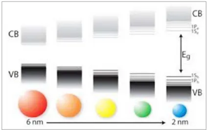
Silicon nanocrystals, like that depicted in Fig. 5(a), are constituted by an ensemble of few atoms, being their typical sizes few nanometer wide. This implies that, as long as the dimensions are scaled down, the energy level distribution changes, becoming more similar to a discrete energy level distribution, which results into an enlargement of the energy band gap (Fig. 6). The size dependence of the energy gap is at the basis of the concept of bandgap engineering, which allows the tunability of the optical emission through the control of the size. Since bulk Si bandgap falls in the IR, being equal to 1.13 eV, the energy gap shifts towards the visible range.
9
Fig. 6. Illustration of bandgap enlargement and discretization of the energy levels induced by
the decreasing of the size.
As a consequence, the occurrence of QC effects can be probed via the combined use of high resolution imaging techniques (such as Transmission Electron Microscopy) and photoluminescence measurements. The enlargement of the energy bandgap induces the shift of PL peak towards lower wavelengths with reducing the size, while the increasing of the radiative recombination probability leads to an enhancement of the intensity yield [Barbagiovanni11, Priolo14]. The blueshift of the optical emission in shown in Fig. 5(b) in the case of decreasing SiNC mean diameter.
More recently, SiNWs [Fig. 7(a)] have been targeted as a highly attractive component for optoelectronic devices owing to the tunability of their optoelectronic properties through the control of their size. Indeed, a blueshift of the PL peak with decreasing the diameter, as shown in Fig. 7(b), was ascribed to the QC of electrical carriers in two dimensions [Zhao04,
Irrera12]. In literature, further studies of the electronic energy gap of very thin semiconducting nanowires confirmed the occurrence of QC effects in SiNWs [Ma03].
10
Fig. 7. (a) SEM image of SiNWs synthesized via metal assisted chemical etching; (b) PL
emission of SiNWs with different size [Irrera12].
1.2.b Correlation between theoretical models and experimental results
In literature, to calculate the electronic structure in Si nanostructures, the density functional theory has been applied. This approach requires the determination of the electronic density of states and the knowledge of the electronic wave states. In perturbative effective mass approximation (EMA) the reduction of the dimensions is introduced as a perturbation to the bulk energy [Barbagiovanni12]. In practice, both electrons and holes are considered like particles in a box, where the amplitude a of the box is given by:
(1)
which represents the Bohr radius. Here is the effective mass of the electron (hole), e is the electric charge, is the dielectric constant. It is possible to individuate three regimes [Barbagiovanni12]:
11 -weak confinement, if the dimension of the system is much larger than both
and
-medium confinement, if the dimension of the system is much smaller than
but larger than so that only the electrons experience QC;
-strong confinement, if the dimension of the system is much smaller than both and
In EMA approach the energy levels are calculated starting from the Hamiltonian of a system of Coulombic interacting particles. The main characteristics of EMA relies in the choice of the basis set, which is expanded to reflect the use of an infinite confinement potential with a Bloch basis. Assuming the effective masses of the electrons and holes calculated using the DOS (me=1.08 and mh=0.57) and 11.8, the calculation of the energy states leads to a quadratic dependence of the energy gap Egap with respect to the diameter of SiNCs:
(2)
where E(∞) is the bulk energy bandgap, while the values of the parameter A take into account the effect of strong, medium or weak confinement and can be found in ref. [Barbagiovanni12]. Hence, the main result of EMA approach relies in the dependence of the Egap on the inverse of the square of SiNC diameter. This model has been applied to describe the QC in SiNCs embedded in SiO2 synthesized via ion-implantation and microwave-plasma-decomposition as well as in SiNCs embedded in SiN [see Fig. 8, extracted from ref. Barbagiovanni12]. EMA provides an enough-simple approach to solve the energy level distribution in Si nanostructures.
12
Fig. 8. Crystalline and amorphous Si-Quantum Dots data and theoretical behavior predicted
with EMA approach. ‘Expt. Ion-Implantion Siτ2’ refers to crystalline Si QDs embedded in
SiO2 [Mokry09]. ‘Expt. microwave plasma decomposition (MPD) Siτ2’ refers to crystalline
Si QDs embedded in SiO2 [Takagi90]. ‘Expt. plasma enhanced chemical vapor deposition
(PCVD) Siσ’ refers to amorphous Si QDs embedded in SiN [Park01]. Theoretical fits for
strong and medium confinement are also shown considering Egap(∞) = 1.12 or 1.56 eV (as
labeled) in Eq. (2) [Barbagiovanni12].
A slightly more sophisticated approach considers the calculation of the electronic structure of Si crystallites using the linear combination of atomic orbitals (LCAO) methods [Delerue93]. In this case, the dimensional dependence of the bandgap energy exhibits an exponent equal to 1.39
(3)
where is eV and D is expressed in nm; the last two terms take into account a correction due to the change of the lattice parameter as a function of the size [Ledoux00]. This law accounts quite well for the experimental behavior of SiNCs with very narrow size distribution [Ledoux00], so that a strict correlation between the size and the optical emission of SiNCs can be attained. This constitutes the basis to understand the optical response of an ensembles of SiNCs with different sizes, typically given by a broad PL spectrum. Indeed, after the deconvolution of the PL peak into given spectral
13 components, each component can be correlated with a given SiNC size through the Eq. (4).
Concerning QC in SiNWs, experiments and ab-initio studies have been performed on hydrogen-passivated SiNWs. Zhao et al. [Zhao04] employed the density functional theory with the local density approximation and the many-body perturbation method based on the Green's function (GW) approximation to calculate the energy bandgap of hydrogen-passivated SiNWs oriented along both [110] and [111] directions. Since the effective mass in the confinement plane for the [111] wires is smaller than for the [110] wires, the energy upshift is expected to be larger for the [111] wires. Hence, in addition to a size dependence, the energy gap also depends on the NW growth direction. Moreover, calculations performed on SiNWs oriented along the [110] direction were corrected by evaluating the self-energy operator in the GW approximation (filled squares in Fig. 9). By fitting these data points with the function:
(4)
where is the bulk gap value and D is the NW diameter, the fit is compatible with the experimental point measured by Ma et al. [Ma03] (symbol * in Fig. 9). Ma et al. [Ma03] performed also a study of the electronic properties of H-terminated SiNWs oriented along the [112] direction by using scanning tunneling spectroscopy (STS) measurements to evaluate their electronic bandgap (symbols + in Fig. 9). It can be seen from Fig. 9 that the bandgap for the SiNW having diameter equal to 7 nm is close to Si bulk value at 1.1 eV, and it increases first gradually and then steeply to a much larger value of 3.5 eV as the diameter decreases to 1.3 nm.
14
Fig. 9. Local density approximation based calculations of the band gaps for [110] (empty
squares) and [111] (empty circles) wires, and the GW-corrected gaps (filled squares) for the two thinnest [110] wires, compared with the measured gaps for [112] wires (+) and a [110] wire (*). The dotted, dashed, and continuous lines are fitted to the data points [Zhao04].
Finally, a comparison between the optoelectronic properties shown by SiNCs and SiNWs can be drawn. It can be noted that the onset of QC effects is restricted to ultra-thin SiNW diameters, while it is slightly relaxed for SiNCs. This effect can be explained if one considers that in wire systems the confinement is limited only to two dimensions whereas clusters are 0D systems confined in all the three dimensions.
1.3. Context and objectives of the PhD Thesis
This PhD project has being conducted in the framework of a co-tutelle agreement between the Physics and Astronomy Department of the University of Catania (Italy) and the Institut National de la Recherche Scientifique-Centre Énergie, Matériaux et Télécommunications (INRS-EMT, Varennes, Canada). A significant part of the research was conducted within the Institute for Microelectronics and Microsystems of the National
15 Research Council (IMM-CNR, Catania). Moreover, this collaborative program involved also the University of Rome “Tor Vergata” and Tekna Plasma Systems Inc. (Sherbrooke, Canada).
The aim of the work was devoted to the investigation of the properties of Si based nanopowders found as a by-product during the inductively coupled plasma (ICP) process, usually performed by Tekna for the production of silicon microspheres. To this purpose, three classes of Si nanostructures have been extensively studied, namely SiNWs, chapelet-like Si nanostructures and SiNC chains, produced by the novel technique of ICP. Focus has been put on the correlation between the structural characterization of the Si nanostructures and their optical properties, in order to understand the occurrence of QC effects related to their nanosize. In this field, the knowledge of the state of the art in Si nanostructures synthesis approaches as well as the theoretical basis and the practical use of TEM-related techniques have been paramount.
In summary, an overview of the growth mechanisms at the basis of SiNW formation will be discussed in the second chapter, where also an extensive panorama of synthesis techniques currently employed for SiNW production is presented. More importantly, the difference between the experimental characteristics of the techniques and the physical/chemical mechanisms underpinning the SiNW assembly is pointed out. In the third chapter, the experimental equipment used for the synthesis of ICP-nanostructures and their structural, chemical and optical analyses are presented. The main results concerning the investigation of ICP-SiNWs will be illustrated in the fourth chapter, where the two competitive growth mechanisms driving the growth of SiNWs are detailed. Finally, the visible to near-infrared broad photoluminescence of these ICP-SiNWs is shown and correlated with their TEM revealed nanostructural characteristics. In the fifth chapter, the optimized purification process that has been developed for the extraction of SiNWs from the by-product powder is described. In the sixth chapter, the effects of post-thermal annealing treatments on the nanostructural changes of SiNWs have been studied. In this way, we were able to reach the Rayleigh instability conditions and structurally transform the SiNWs into a more intriguing Si nanocomposite, made by SiNCs wrapped in a silica wire. Finally, the novel procedure developed by Tekna
16
for the intentional synthesis of SiNWs via ICP is outlined as a new perspective which opens the route for the high-throughput production of ICP-SINWs.
Bibliography
[Barbagiovanni11] E. G. Barbagiovanni, L. V. Goncharova, and P. J. Simpson, Phys. Rev. B 83, 035112 (2011).
[Barbagiovanni12] E. G. Barbagiovanni, D. J. Lockwood, P. J. Simpson and L. V. Goncharova, J. Appl. Phys. 111, 3 (2012).
[Bonafos04] C. Bonafos, M. Carrada, N. Cherkashin, H. Coffin, D. Chassaing, G. B. Assayag, A. Claverie, T. Müller, K. H. Heinig, M. Perego, M. Fanciulli, P. Dimitrakis and P. Normand, J. Appl. Phys. 95, 10 (2004).
[Canham90] L. Canham, Appl. Phys. Lett. 57, 10 (1990).
[Chan08] C. K. Chan, H. Peng, G. Liu, K. McIlwrath, X. F. Zhang, R. A. Huggins and Y. Cui, Nat. Nanotech. 3, 1 (2008).
[Cullis97] A. G. Cullis, L. T. Canham, and P. D. J. Calcott, J. Appl. Phys. 82, 3 (1997).
[Delerue93] C Delerue, G Allan, M Lannoo, Phys. Rev. B 48, 15 (1993). [Dogan16] I. Dogan and M. C. M. van de Sanden, Plasma Process. Polym. 13, 1 (2016).
[ENIAC07] European Nanoelectronics Initiative Advisory Council (ENIAC), Strategic Research Agenda, 2007 Edition.
[Franzò08] G. Franzò, M. Miritello, S. Boninelli, R. Lo Savio, M. G. Grimaldi, F. Priolo, F. Iacona, G. Nicotra, C. Spinella, and S. Coffa, J. Appl. Phys. 104, 9 (2008).
17 [GlobalInfoInc14] Global Information Inc. (2014), Nanotechnology, Freedonia Group, CT, USA.
[Hochbaum08] A. I. Hochbaum, R. Chen, R. D. Delgado, W. Liang, E. C. Garnett, M. Najarian, A. Majumdar and P. Yang, Nature 451, 7175 (2008). [Iacona04] F. Iacona, C. Bongiorno, C. Spinella, S. Boninelli, and F. Priolo, J. Appl. Phys. 95, 7 (2004).
[Irrera12] A. Irrera, P. Artoni, F. Iacona, E. F. Pecora, G. Franzo, M. Galli, B. Fazio, S. Boninelli and F. Priolo, Nanotechnology 23, 7 (2012).
[Koole14] R. Koole, E. Groeneveld, D. Vanmaekelbergh, A. Meijerink and C. Donegá, Chapter 2 in Nanoparticles – Workhorses in Nanoscience,
Springer-Verlag Berlin Heidelberg (2014).
[Kovalev98] D. Kovalev, H. Heckler, M. Ben-Chorin, G. Polisski, M. Schwartzkopff and F. Koch, Phys. Rev. lett. 81, 13 (1998).
[Ledoux00] G. Ledoux, O. Guillois, D. Porterat, C., Reynaud, F. Huisken, B. Kohn and V. Paillard, Phys. Rev. B 62, 23 (2000).
[Li04] Z. Li, Y. Chen, X. Li, T. I. Kamins, K. Nauka and R. S. Williams, Nano Lett. 4, 2 (2004).
[Lofaro15] M. J. Lo Faro, C. D’Andrea, E. Messina, B. Fazio, P. Musumeci, R. Reitano, G. Franzò, P. G. Gucciardi, C. Vasi, F. Priolo, F. Iacona and A. Irrera, Sci Rep. 5, (2015).
[Ma03] D. D. D. Ma, C. S. Lee, F. C. K. Au, S. Y. Tong, S. T. Lee, Science 299, 5614 (2003).
[MarketOutlook15] RNCOS E-Services Pvt. Ltd. 2015, Global Nanotechnology Market Outlook 2022. Research Report, Can-Biotech Inc., Canada.
[McAlpine07] M. C. McAlpine, H. Ahmad, D. Wang and J. R. Heath, Nat. Mater. 6, 5 (2007).
18
[Mokry09] C. R. Mokry, P. J. Simpson, and A. P. Knights, J. Appl.Phys. 105, 11 (2009).
[Park01] N. M. Park, C. J. Choi, T. Y. Seong, and S. J. Park, Phys. Rev. Lett. 86, 13 (2001).
[Pavesi10] L. Pavesi and R. Turan, Silicon nanocrystals: fundamentals, synthesis and applications. John Wiley & Sons (2010).
[Priolo14] F. Priolo, T. Gregorkiewicz, M. Galli and T. F. Krauss, Nat. Nanotech. 9, 1 (2014).
[Takagi90] H. Takagi, H. Ogawa, Y. Yamazaki, A. Ishizaki, and T. Nakagiri, Appl. Phys. Lett. 56, 2379 (1990).
[webinfo] http://www.telegraph.co.uk/technology/2016/02/25/end-of-moores-law-whats-next-could-be-more-exciting/.
[Wen15] X. Wen, P. Zhang, T. A. Smith, R. J. Anthony, U. R. Kortshagen, P. Yu, Y. Feng, S. Shrestha, G. Coniber and S. Huang, Sci. Rep. 5 (2015). [Xu12] C. Xu, Process optimization for the 3D sequential integration of FDSOI CMOS transistors, PhD thesis, Grenoble University (2012).
[Zacharias02] M. Zacharias, J. Heitmann, R. Scholz, U. Kahler, M. Schmidt, and J. Bläsing, Appl. Phys. Lett. 80, 4 (2002).
[Zhao98] J. Zhao, A. Wang, M. A. Green and F. Ferrazza, Appl. Phys. Lett. 73, 14 (1998).
[Zhao04] X. Zhao,C. M.Wei,L. Yang and M.Y. Chou, Phys. Rev. Lett. 92, 23
19
2. Growth
mechanisms
of
Si
nanowires and their associated
synthesis techniques
In this chapter the fundamental concepts and the state of the art on the Si nanowire (SiNW)-related research, that is at the basis of the present work, will be presented. It will address the treatment of SiNWs by doing the distinction between the growth mechanisms and the experimental techniques for their synthesis. Indeed, the structural and the optical investigation of SiNWs produced via the innovative Inductively Coupled plasma (ICP) technique has been pursued to understand their growth mechanism, in order to better control the SiNW production by means ICP. In this perspective, it could be advantageous to preliminary give an overview of the most well-established growth mechanisms of Si nanostructures and their associated synthesis techniques. These aspects will be treated in the first and second paragraphs, respectively.
2.1. Growth Mechanisms for SiNW formation
The description of the mechanisms ruling the growth of nanostructures, and in particular of SiNWs, relies on the fact that their formation is induced by physical and chemical driving forces. The investigation of the mechanisms that lead to their assembly is the object of
20
this paragraph, where the distinctions between the so-called Vapor-Liquid-Solid (VLS) growth mechanism and the Oxide Assisted Growth (OAG) of one-dimensional (1D) Si nanostructures are elucidated.
2.1.a Vapor-Liquid-Solid mechanism
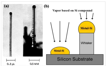
Although the first report on filamentary Si structures traces back to the publication of Treuting and Arnold [Treuting57], the pioneering work of Wagner and Ellis [Wagner64] sets the basis for the research on 1D Si nanostructures growth. Even though the dimensions of the 1D Si whiskers they investigated were quite large [Fig. 1(a)], being of the order of 100 nm or even more, they opened the route towards the synthesis of innovative 1D nanostructures, since they clarified the growth mechanism responsible for the formation of these nanostructures. Indeed, the observation of no screw dislocations along the axial direction of the Si whiskers led them to conclude that the anisotropic growth was attributable to the catalytic action of metallic impurities, previously deposited on a Si substrate, and not driven by the possible presence of dislocations [Wagner64].
Their claim relies on two main facts:
a) no growth occurs in absence of the metallic particles; b) the Si whiskers present a metallic particle at their tip.
Hence, they explained the growth of the Si structures in terms of the so-called VLS mechanism. Since then, VLS mechanisms has represented the most common way to synthesize 1D Si structures and further efforts have been devoted to produce thinner and thinner Si whiskers, so the term of “Si nanowires” has been adopted [Wang08, Schmidt09, Schmidt10].
21
Fig. 1.(a) Si whiskers synthesized via VLS mechanisms, firstly reported by Wagner and Ellis.
[Wagner64]. It can be noted that the lateral dimensions were quite big, up to 0.2 mm. (b) Schematic of the 1D Si nanostructures growth via VLS.
A schematic of the VLS mechanisms is illustrated in Fig. 1(b). In the VLS mechanism, a Si compound in the vapor phase represents the precursor that supplies the Si material and is provided in the reaction chamber during the growth. A solid Si substrate is previously introduced into the chamber, whereas some metallic particles are present on the substrate surface. The metallic particles can be formed either in a previous step before the introduction of the substrate into the chamber [Schmidt09], or in situ prior to SiNW growth [Wang06]. The gaseous precursor impinges on the solid Si substrate, but is preferentially decomposed in correspondence of the metallic particles, because of their catalytic action. In this way, Si atoms are incorporated into the metallic particles, which are liquid at the experimental conditions set for the growth. More precisely, Si incorporation in the metal leads to the formation of a metal-Si alloy. At the eutectic point, which corresponds to the experimental conditions set for the growth, the alloy is in liquid phase. Further absorption of Si atoms led to the supersaturation of Si in the alloy, thus precipitation of Si atoms occurs, then the Si atoms deposit layer-by-layer right under the droplet in a crystalline arrangement.
22
Fig. 2. Phase-diagrams of some metal-Si alloys exploited for the synthesis of SiNWs: (a) Au,
23 In this way, 1D structures form only below the metallic particles, as sketched in Fig. 1(b). whereas negligible crystal growth takes place in correspondence of the other regions of substrate.
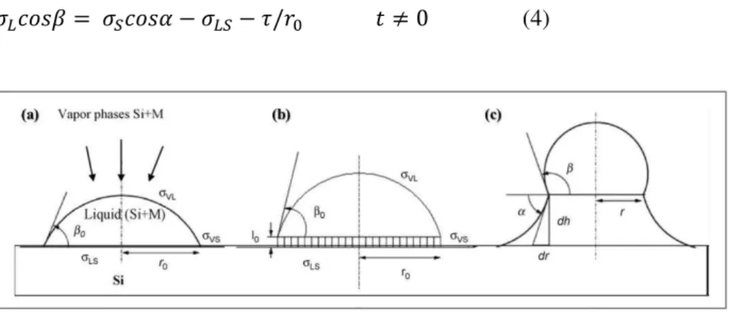
More general theoretical models have been developed to describe the anisotropic growth of a Si crystal based on the presence of a catalytic mediator [Wacaser09]. Indeed, it has been observed that, similarly to a VLS mechanism, 1D growth can occur even if the metallic particle is solid during the growth [Wang06], or also in liquid and superfluid media [Davidson07, Tuan05]. These mechanisms are denoted as Vapor-Solid-Solid (VSS) and solution–liquid–solid (SLS) or supercritical-fluid–liquid-solid (SFLS) respectively [Wacaser09]. Moreover, vapor–adsorption-layer–solid [Bootsma71] and solid-liquid-solid mechanisms [Yu01] have been reported as well. In all these cases, the main driving force inducing SiNW formation can be described within the frame of a more general three-phase mechanism [Wacaser09]. The knowledge of binary metal-Si phase-diagrams (PD) is a fundamental prerequisite for the understanding of all these mechanisms, in particular to fix the temperature and the Si concentration corresponding to the eutectic point. The phase diagram also establishes whether the particle is liquid or solid at the experimental conditions set for the growth. The PDs of some of the most exploited metal catalysts for SiNW synthesis are shown in Fig. 2. It should be noted that, in general, for the eutectic alloys the lowering of the melting point with respect to the melting point of the single elements occurs. The theoretical description of the growth process can be developed fixing the three phases as for the VLS [Wang08]. So, if we indicate L, S, LS as the surface tensions of the liquid, the solid and the liquid-solid interface respectively (Fig.3), we can set the following balance equation:
(1)
the time t=0 indicates that this equation holds prior to the SiσW growth. β is the angle defined by the substrate surface and the perpendicular to the droplet at its contact point, so it is also called contact-angle and it is such that:
24
where r0 is the radius of the contact area and R is the radius of the droplet. A more clear vision of these physical quantities can be provided by the Fig. 3(a). An approach that takes into account the nanosize of the materials has been demonstrated to lead to an additional term to Eq. (1) [Rowlinson03]:
(3)
where is the line tension, defined as the excess of free energy per unit length calculated along the contact line of the three phases [Widom95]. Such a contact line is a circle of radius r0, as it is clarified by Fig. 3(a). After the transient time, when the first Si crystalline monolayer is formed [Fig. 3(b)], the SiNW grows. During the growth, it can be observed that the radius of the contact area diminishes, while the droplet approaches a spherical shape and nanowire flanks enlarge, in such a way that an angle α is formed, as it can be seen in Fig. 3(c). So, at t ≠ 0 the Eq. (3) becomesμ
(4)
Fig. 3. (a) Condition at t=0; (b) early stage of SiNW growth, where the first Si crystalline
monolayer is formed; (c) equilibrium condition for SiNW growth [Wang08].
The kinetics of NW growth is controlled by the so-called Gibbs-Thomson effect [Givargizov75], for which the growth rate is faster for larger-diameter NWs. Indeed, since the Gibbs-Thomson effect, the growth rate V is expressed as:
25
(5)
being the difference between the chemical potential of Si in the vapor phase and in the 1D crystal, while Ω is the atomic volume of Si, η is the island edge energy, K is the Bolzmann constant, T the temperature and h is the layer thickness. is related to the diameter of the wire by the relation [Wang08]:
(6)
where 0 corresponds to the chemical potential when d→∞. represents the driving force for the SiNW growth. We can note that, since Δ is given by the Eq. (6), V is enhanced for larger values of d.
Nevertheless, it should be remarked that for ultra-thin SiNWs, when the growth is limited by the Gibbs-Thomson effect, diffusion phenomena become important. Hence, not only Si atoms are incorporated and precipitate in the metallic droplet [Fig. 4(a)], but Si adatoms coming from the source can also diffuse on the substrate and be incorporated in the SiNW [Fig. 4(b)]. This type of SiNWs shows typically an enlargement at the NW basis, which is called “tapering” and is due to the uncatalysed deposition of Si on the sides of the nanowires at higher T [Wang06]. It should be added that, especially at low T, Si adatoms can diffuse on the metallic particle surface [Fig. 4(c)], which is solid because of the low T condition. In this last condition the growth rate results [Cai07, Neumann72, Wang57]:
(7)
where represents the surface concentration gradient of Si in the metal and is the surface diffusion coefficient.
26
Fig. 4. (a) Adsorption of Si atoms in the droplet; (b) diffusion of Si atoms on the metallic
particle and incorporation of Si at the liquid-solid interface; (c) diffusion of the Si atoms on the substrate and incorporation at the SiNW flanks [Wang08].
It will be demonstrated in the fourth chapter that a small percentage of ICP-SiNWs form according to the VLS model, whereas Fe particles act as the catalyst that induced their growth.
2.1.b Oxide Assisted Growth mechanism
Oxide Assisted Growth mechanism was also identified as a valid alternative to synthesize SiNWs without resorting to any metal catalysts [Zhang03]. Indeed, in the OAG mechanism, instead of the metal catalyst, silicon suboxide clusters have the main role in inducing the growth of the SiNWs. These Si suboxide clusters constitute the vapor of an ablated or evaporated SiO2-containing Si target. The main reactions at the basis of the OAG are the following [Wang08]:
Si (solid) + SiO2 (solid) → 2 Siτ (gas) (a) 2Siτ (gas) → Si (solid) + Siτ2 (solid) (b) Sixτ (gas) → Six-1 (solid) + SiO (solid), x>1 (c)
27 Reaction (a) occurs at temperatures higher than a thousands of °C, in order to achieve the complete evaporation of the SiO2 containing target [Lamoreaux86]), while reactions (b) and (c) occur at lower temperatures (850°-1100°C) [Lee00, Peng01,Zhang03]. Zhang and co-workers conducted an intriguing OAG experiment in two steps to demonstrate the role of the silicon oxide, [Zhang03]: previously a SiO2-containing Si target was ablated to induce the nucleation of the SiNWs, then a Si target (without any SiO2 source) was ablated to continue the growth. Nevertheless, no further growth occurred in the second step. So, unlike the VLS growth, where the growth is sustained as long as the Si vapor is supplied, no OAG occurs when only a Si target is used. Furthermore, observations report that VLS and OAG can also coexist in the same process as long as metal catalyst and SiO2 are provided in the target [Peng01, Zhang03].
In literature, the composition of the gas phase formed by reaction (a) has been investigated theoretically [Zhang01, Zhang04]. Si suboxide clusters are highly reactive and tend to bond with other clusters preferentially forming a Si-Si bond. Nevertheless, the richest of Si is a Si-suboxide cluster, the highest is the cohesion energy per atom; hence, Si-rich Si-suboxide clusters are not favored in the gas phase. Indeed, it has been calculated that the formation of SiNWs is favored at the ratio of Si to O close to one [Zhang01]. Experimental and theoretical works revealed that silicon monoxide clusters adopt buckled-ring or planar configurations [Wang08]. An example of the earliest stages of nucleation in OAG is shown in Fig. 5. In Fig. 5(a) a SiO cluster is illustrated with a buckled-ring configuration having a number n=3 of Si atoms (and hence three O atoms). Thus, the nucleation proceeds by further aggregation of the SiO units [Fig. 5(b)]. It has been calculated that starting from n = 5 the most stable configuration contains a Si core surrounded by a silicon oxide shell, indeed the open circles containing stars in (c) represent the Si atoms constituting the Si core. In Fig. 5 it is also easily demonstrated that the formation of an inner Si core involves Si atoms with three and four coordinates as n increases, leading to a more stable cluster.
28
Fig. 5. Early stages of SiO-like clusters aggregation, which evolves from the buckled-ring
configuration (a and b) to the formation of a Si core surrounded by a silicon oxide shell (c-j). The open circles containing stars in (c) represent the Si core surrounded by a silicon oxide shell. The crystalline arrangement is most favored after n=18 (i) [Wang08].
Indeed, at n = 18 [Fig. 5(f)] all of the Si atoms belonging to the Si cores are four-coordinated in the sp3 configuration of crystalline Si. In the graph reported in Fig. 6 it is depicted the most favorable structure in which the Si-suboxide clusters aggregate, while the number n of SiO units increases [Wang08]: the circles represent the buckled-ring configuration while the triangles represent the Si-Si oxide core-shell structure. It can be seen that the buckled-ring configuration becomes less favorable at n=5, while the core-shell structure is the most stable configuration at higher number of SiO units.
29
Fig. 6. Binding energy (eV/atom) of (SiO)n clusters vs. the number n of SiO units. The
triangles are (SiO)n with the Si-core structure surrounded by a silicon oxide sheath and open
circles are those with buckled-ring structure [Wang08].
Figure 7 illustrates the isomers of the SiO clusters with the O atom in different locations, from the center [Fig. 7(a)] to the surface [Fig. 7(c)] as well as the corresponding binding energy [Wang08]. It can be noted that the configuration with the O at the surface corresponds to the most stable configuration. This is in agreement with the observation that OAG-SiNWs possess a core-shell Si-silicon oxide configuration. O atoms could simply diffuse from the center to the surface via bond switching [Fig. 7(b)].
30
Fig. 7. Isomers of the SiO clusters with the O atom (in yellow) in different locations: (a) at the
center of the cluster, (b) at intermediate position, (c) at the cluster surface. The associated binding energies for each configuration is also displayed [Wang08].
This results in the formation of an outer silicon oxide shell during the Si-suboxide cluster aggregation, i.e. the nucleation of the SiNWs. Let us notice that for SiNW nucleation, the temperature should be lower than the initial temperature needed for the formation of the Si-suboxide cluster based vapor, as also remarked in the reactions (b and c). Hence, the temperature gradient represents the external driving force for OAG-SiNW formation. Generally, the OAG mechanism has been reported for synthesis temperatures between 850°-1100°C [Lee00, Peng01, Zhang03].
31
Fig. 8. (a) Sketch of the OAG mechanism. (b)TEM image of Si nanoparticles precipitate from
the decomposition of SiO matrix. (c) The nanoparticles in a preferred orientation grow fast and form nanowires. (d, e) OAG model for the nucleation and early stages of the growth of SiNWs [Lee00].
Once the mechanism of Si-suboxide cluster aggregation has been elucidated, the growth of SiNWs via OAG mechanism can be described as follows [see Fig. 8(a)]. A SiO2-containing Si target is used to produce a vapor constituted of Si and O, which is most likely composed of Si-suboxide clusters that tend to form preferentially bonds with Si. Thus, a Si-suboxide cluster can form a Si-Si bond with a silicon based substrate [Fig. 8(b and d)], becoming thereby a nucleation site for the subsequent growth of nanowires [Fig. 8(c and e)]. Such a nucleated Si-suboxide cluster is fed by the adsorption of additional reactive Si suboxide clusters from the vapor, through the formation of Si-Si bonds. On the other hand, the oxygen atoms in these piled silicon suboxide clusters are laterally expelled by the silicon atoms to the edges where they form a chemically inert SiO2 shell. Such a SiO2 sheath around the SiNW prevents its lateral growth and leaves the only possibility of the perpendicular growth of the Si nanowires [Zhang03]. Remarkably, among the advantages of the OAG based growth, SiNWs were produced with diameters much thinner (i.e. minimum diameter 1.3 nm [Ma03]) than the VLS grown ones (minimum diameter 3 nm [Wu04]). Moreover, the diameter of OAG SiNWs is almost uniform because it is controlled by the self-decomposition of SiO [Wang08].
32
2.2. Conventional techniques for SiNW synthesis
The development of techniques for the synthesis of Si nanostructures aims to achieve a high level of control of the morphological properties and high yield, by suitable design of specific apparatus and methods. Although different techniques have been employed so far, basically it is possible to classify them into two main paradigms: bottom-up and top-down approaches. While the top-down methodology is intended to create the desired nanostructure starting from the bulk material, bottom-up approach conceives the single atoms or molecules as building-blocks to assemble in order to realize suitable nanomaterials. Conventional manufacturing processes in Si-based microelectronics have been led by the top-down paradigms, which basically rely on lithography and etching procedures [Schmidt09]. From the other hand, bottom-up routes have been established as good strategies to fabricate ultra-small structures according to the ongoing trend in the scaling down of devices’ dimensions.
As far as SiNWs are concerned, both top-down and bottom-up synthesis routes have been exploited. Bottom-up methods include chemical-physical approaches, like Chemical Vapor Deposition (CVD) [Hofmann03, Yao05], Molecular Beam Epitaxy (MBE) [Schubert04], laser ablation [Morales98, WangPRB98, WangCPL98, Zhang98] and thermal evaporation [WangPRB98, Wang99]. All these methods will be treated in more detail in this section. CVD and MBE basically rely on a three-phase mechanism, which exploits the presence of a metal acting as a catalyst in the process, according to the VLS process. On the other hand, during laser ablation and thermal evaporation both a metal-catalyzed and a metal-free process can occur, being the former induced by VLS and the latter by the OAG mechanism [Schmidt09, Schmidt10]. A schematic of the most common bottom-up techniques usually employed to produce SiNWs is shown in Fig. 9.
33
Fig. 9. Schematic of the bottom-up techniques used for the synthesis of SiNWs: (a) Chemical
Vapor Deposition, (b) Annealing in reactive atmosphere, (c) Thermal Evaporation of SiO, (d) Molecular Beam Epitaxy, (e) Laser Ablation, (f) Synthesis in solution [Schmidt09].
2.2.a Chemical Vapor Deposition
Chemical Vapor Deposition is usually performed in a tubular hot wall reactor, connected to an externally heated quartz tube where an inert gas, such as a hydrogen gas or a hydrogen/inert gas mixture, flows as a carrier gas [Schmidt09, Schmidt10]. Indeed, along the tube it is located a bubbler filled with a Si-based vapor precursor, which supplies the Si at usual flows rate of about 1500 sccm [Wang08]. Typical precursors are SiH4
34
(silane), Si2H6 disilane, SiH2Cl2 (dichlorosilane) and SiCl4 (tetrachlorosilane) [Schmidt10].
Fig. 10. Typical Scanning Electron Microscopy (SEM) image of SiNWs synthesized via CVD
[Hofmann03].
A Si substrate is located in the reactor and, as long as metallic particles are deposited on the substrate, SiNW growth occurs through the four different steps described by the VLS mechanism, i.e. by (i) breaking of the vapor molecules at the catalyst surface, (ii) Si atom incorporation in the catalyst, (iii) Si precipitation in the form of a crystalline anisotropic structure, and (iv) layer by layer growth below the catalytic particle. Metal particles are formed on the Si substrate because of a temperature-induced dewetting mechanism [Wang08]. More precisely, a metal thin film, deposited on the substrate via sputtering or thermal evaporation, is subject to an annealing treatment (typically at T~500° for Au thin films), which induces the rolling up of the film into small particles to minimize the surface energy. Thicker films dewet in larger nanoparticles. Film deposition via thermal evaporation as well as annealing-induced dewetting can be performed in-situ in the CVD chamber prior to SiNW growth [Wang06]. Metal nanoparticles can be also formed by lithography pattern, followed by annealing. Whatever procedure to obtain nanoparticles on the substrate is adopted, it is important that the particle totally wets the surface, otherwise the crystalline SiNW does not have
35 orientation relationship with the substrate and grow randomly on it [Wang08]. Typical SiNWs grown by CVD are reported in Fig. 10. In literature, wire diameters from a few nanometers up to several micrometers have been reported [Schmidt10], whereas the minimum diameter for SiNWs grown via CVD process was observed to be ~3 nm [Wu04]. Being this diameter dictated to some extent by the metal catalyst, it seems to be the lowest limit achievable for SiNW obtained via CVD.
2.2.b Molecular Beam Epitaxy
Similarly to CVD, MBE relies on the VLS mechanism [Schmidt09, Schmidt10]. The main difference is due to the fact that Si supply does not derive from the decomposition of a Si-based compound in the vapor phase, but Si vapors are provided by Si effusion cells. Therefore, Si atoms impinge on the substrate surface, being preferentially incorporated in the metallic droplets, which have been deposited on the Si substrate in a preparatory step as described above for CVD technique. In literature, an extensive debate has been stimulated on the role of the metallic droplet, being its catalytic role not required in presence of an atomic source which does not need to be decomposed [Schmidt10].
36
As a matter of fact, the NW epitaxial growth is 2 orders of magnitude faster in correspondence of the metal particles than above the uncovered substrate because the metal has merely the role to favor the Si crystallization and lower the chemical potential of the source atoms [Schmidt10]. Moreover, typically the substrate is heated at temperatures of 500°C-700°C. In these conditions, the Si atoms impinging on the substrate are favored to diffuse towards the metallic nanoparticles, so not only the flux of Si atoms coming from the effusion cell, but also the flux of Si adatoms diffusing on the surface control the SiNW growth [Schmidt09]. Another feature of MBE technique is that it is an UHV-based process (pressure of the order of 10-10 mbar), therefore the products synthesized by MBE show high purity in terms of contaminants and oxidation. Nonetheless, the growth rate is quite low for MBE, being of the order of 1-10 nm/min. As a consequence, due to the Gibbs-Thomson effect, larger diameter SiNWs are favored to form, as it can be inferred from the Fig. 11. Indeed, typical diameters larger than 40 nm have been observed [Schmidt09]. Another reason which explains the occurrence of large SiNWs concerns the fact that Ostwald ripening of metallic droplets can occur at the substrate, thus influencing the SiNW diameter by increasing the metallic particle dimensions [Schmidt10]. A part from the slow growth rate, the limited aspect ratio of the SiNWs is affected also by the growth of the substrate induced by those Si atoms that are not able to diffuse toward the nanowires during the growth, but crystallize on the substrate surface [Schmidt10]. Among the advantages of MBE it should be mentioned the high-purity of MBE-grown SiNWs and the possibility to dope NWs in a controlled manner during the growth [Schmidt09].
2.2.c Laser ablation
Like MBE, laser ablation is a physical method which employs a high-power pulsed laser, such as Nd:YAG or KrF excimer laser, to ablate a target [Wang08]. Since the target contains the metal catalyst, the catalyst is coablated with the Si, inducing the Si vaporization as well as metal/metal silicide nanoparticles production in the vapor. Once the Si vapor is dissolved into the nanoparticle, SiNW growth can occur during the vaporization,
37 according to the VLS mechanism. VLS-grown SiNWs by means of laser ablation have as typical feature the catalytic particle at their tip, as it can be seen in Fig. 12(a) [Wang08]. The presence of the substrate is not mandatory for laser ablation because the SiNWs can also deposit on the wall of the reaction chamber [Wang08].
Fig. 12. (a) SiNWs grown by means of laser ablation via the VLS mechanism, as indicated by
the presence of particles at the top of the wires, as marked by the arrow [Wang08]. (b) SiNWs produced in bulk quantity via laser ablation technique [Morales98].
Since the temperatures reached at the target are extremely high, also high-temperature eutectic alloys can be exploited as catalysts for SiNW growth. As an example, Fe has been used for laser ablation VLS-based synthesis [Morales98]. Hence, laser ablation allows high versatility in the choice of the materials, including the ones with higher eutectic temperature, and also doped SiNWs can be realized [Schmidt10].
Furthermore, by mixing SiO2 and Si in the target, an OAG growth driven SiNW synthesis has also been demonstrated via laser ablation [Zhang03]. These nanostructures exhibit an elevate aspect-ratio thanks also to the high growth rates, which has been reported to range from 0.1-1 µm/min up to several µm/min [Schmidt09]. The growth rate depends on different parameters, such as the power of the laser, the vacuum conditions, the gas employed and the temperature [Wang08]. Finally, it is worthy to mention that laser ablation process is conducted inside a furnace as reaction chamber, filled with an inert gas, such as Ar, He, H2, or N2. It has been
38
observed that different choice of the gas influences the final diameter of the SiNWs and thus their optoelectronic properties [Zhang99].
In general, bulk quantity production [Morales98, Zhang98] has been achieved via laser ablation [see Fig. 12(b)], which is one of the main advantage of the exploitation of laser ablation together with the above-mentioned great versatility of this technique. The condition of high temperature generated by the plasma makes laser ablation very similar to the ICP technique used in the present work. Hence, the knowledge of laser ablation is an important requirement for the understanding of SiNWs synthesis via ICP. We will see in the following part that also thermal evaporation possesses similar characteristics to the ICP process.
2.2.d Thermal evaporation
Thermal evaporation is accomplished in a tube furnace connected with an inert gas supply. The experimental conditions are chosen in such a way that a temperature gradient exists, allowing the inert gas to flow from the hotter to the colder part of the tubular furnace [Wang08]. The source is located in the hot zone of the furnace, so that it evaporates and the vapor is carried by the inert gas towards the colder region of the tube, where both a VLS reaction (in case the source contains some metallic components) and a disproportionation reaction (in case the source has a SiO-based composition) can occur [Wang08]. In the first case, VLS-based mechanism drives the growth of the SiNWs, while in the other case the OAG mechanism is at the basis of the growth of the SiNW, like the ones shown in Fig. 13. Typical growth parameters are pressures of the order of 100 Torr, flow rates of inert gas or inert gas/hydrogen mixture of ~50 sccm, temperatures in the range of 1100-1350 °C for the hot part of the reactor and temperatures of 900-1000°C for the colder part of the reactor where Si nanowire growth.
39
Fig. 13. Typical SEM image of SiNWs grown via thermal evaporation [Zhang03].
Thermal evaporation has the important advantage to enable the production of bulk-quantity of SiNWs [Zhang00] with ultra-thin diameter up to ~1.3 nm [Ma03]. From the other hand, the main drawback [Schmidt10] is the lack of controllability in terms of SiNW diameters and lengths. Also, a controlled doping of the nanowires is difficult. As mentioned above, thermal evaporation technique has similar features to the ICP process: indeed, like in thermal evaporation, ICP technique require the evaporation of the target as a fundamental step, which is accomplished by means of high-temperature plasma.
2.3. Conclusions
An overview of the in-lab techniques currently employed for SiNW synthesis has been presented in this chapter, as well as the physical and chemical mechanisms at the basis of SiNW formation. These mechanisms can be essentially based on the catalytic action of a metal particle in a three
40
phase mechanism [Wacaser09] or on the OAG mechanism [Zhao03], where the main role is performed by Si suboxide clusters. The techniques illustrated here basically rely on the bottom-up approach, which has been demonstrated to be more suitable than top-down methods for the synthesis of ultra-thin SiNWs.
Nevertheless, it deserves to be noted that the growth of these ultra-thin structures is challenging, in particular when the SiNW growth occurs via the VLS mechanism, for which the minimum diameter is dictated by the minimum size of the metallic particle. A further issue concerns the yield of SiNW that is provided by the well-established synthesis techniques described above, for which a bulk production is highly desirable.
In this panorama, Inductively Coupled Plasma (ICP) technique, which will be described in the next chapter, appears as a promising technique for the high throughput production of SiNWs.
Bibliography
[Bootsma71] G. A. Bootsma and H. J. Gassen, J. Cryst. Growth 10, 223 (1971).
[Cai07] Y. Cai, Characterization of ultrathin II–VI semiconductor nanowires by transmission electron microscopy, PhD Dissertation, Physics Department, the HongKong University of Science and Technology, HongKong, September 2007.
[Davidson07] F. M. Davidson, D. C. Lee, D. D. Fanfair and B. A. Korgel, J. Phys. Chem. C. 111 (2007).
[Givargizov75] E. I. Givargizov, J. Cryst. Growth 31 (1975).
[Hofmann03] S. Hofmann, C. Ducati, R. J. Neill, S. Piscanec, A. C. Ferrari, J. Geng, R. E. Dunin-Borkowski and J. Robertson, J. Appl. Phys. 94, 9 (2003).
41 [Lamoreaux86] R. H. Lamoreaux, D. L. Hildenbrand and L. Brewer, J. Phys. Chem. Ref. data 16, 3 (1987).
[Lee00] S. T. Lee, N. Wang and C. S. Lee, Mater. Sci. Eng. A 286, 1 (2000). [Ma03] D. D. D. Ma, C. S. Lee, F. C. K. Au, S. Y. Tong and S. T. Lee, Science 299, 5614 (2003).
[Morales98] A. M. Morales and C. M. Lieber, Science 279, 5348 (1998). [Neumann72] G. Neumann, G.M. Neumann, Surface Self-diffusion of Metals, Diffusion Monograph Series, vol. 1, Diffusion Information Center, 1972, p.105.
[PDDatabase] http://steel.kisti.re.kr/htm/Fe-Si.htm.
[Peng01] H. Y. Peng, Z. W. Pan, L. Xu, X. H. Fan, N. Wang, C. S. Lee and S. T. Lee, Adv. Mater. 13, 5 (2001).
[Rowlinson03] J.S. Rowlinson, B. Windom, Molecular Theory of Capillarity, Dover, 2003.
[Schmidt09] V. Schmidt, J. V. Wittemann, S. Senz and U. Gösele, Adv. Mater. 21, 25‐26 (2009).
[Schmidt10] V. Schmidt, J. V. Wittemann and U. Gösele, Chem. Rev. 110, 1 (2010).
[Schubert04] L. Schubert, P. Werner, N. D. Zakharov, G. Gerth, F. M. Kolb, L. Long, U. Gösele and T. Y. Tan, Appl. Phys. Lett. 84, 24 (2004).
[Treuting57] R. G. Treuting and S. M. Arnold, Acta Met. 5, 598 (1957). [Tuan05] H. Y. Tuan, D. C. Lee, T. Hanrath, B. A. Korgel, Nano Lett. 5, 681 (2005).
42
[Wacaser09] B. A. Wacaser, K. A. Dick, J. Johansson, M. T. Borgström, K. Deppert and L. Samuelson, Adv. Mater. 21, 2 (2009).
[Wagner64] R. S. Wagner and W. C. Ellis, Appl. Phys. Lett. 4, 5 (1964). [Wang57] H. Wang, G.S. Fischman, J. Appl. Phys. 76 (1994) 1557.
[WangPRB98] N.Wang, Y. H. Tang, Y. F. Zhang, C. S. Lee and S. T. Lee, Phys. Rev. B 58, 24 (1998).
[WangCPL98] N. Wang, Y. H. Tang, Y. F. Zhang, D. P. Yu, C. S. Lee, I. Bello and S. T. Lee, Chem. Phys. Lett. 283, 5 (1998).
[Wang99] N. Wang, N., Y. H. Tang, Y. F. Zhang, C. S. Lee, I. Bello and S. T. Lee, Chem. Phys. Lett. 299, 2 (1999).
[Wang06] Y. Wang, V. Schmidt, S. Senz, U. Gösele, Nat. Nanotechnol. 1, 186 (2006).
[Wang08] N. Wang, Y. Cai, and R. Q. Zhang, Mater. Sci. Eng. R-60, 1 (2008).
[Widom95] B. Widom, J. Phys. Chem. 99, (1995).
[Wu04] Y. Wu, Y. Cui, L. Huynh, C. J. Barrelet, D. C. Bell and C. M. Lieber, Nano Lett. 4, 3 (2004).
[Yao05] Y. Yao, F. Li and S. T. Lee, Chem. Phys. Lett. 406, 4 (2005). [Yu01] D. P. Yu, Y. J. Xing, Q. L. Hang, H. F. Yan, J. Xu, Z. H. Xi and S. Q. Feng, Phys. E 9, 305 (2001).
[Zhang98] Y. F. Zhang, Y. H. Tang, N. Wang, D. P. Yu, C. S. Lee, I. Bello and S. T. Lee, Appl. Phys. Lett. 72, 15 (1998).
[Zhang99] Y. F. Zhang, Y. H. Tang, H. Y. Peng, N. Wang, C. S. Lee, I. Bello, and S. T. Lee, Apll. Phys. Lett. 75, 1842 (1999).
43 [Zhang00] Y.F. Zhang, Y.H. Tang, C. Lam, N. Wang, C.S. Lee, I. Bello, S.T. Lee, J. Cryst. Growth 212, 1 (2000).
[Zhang01] R.Q. Zhang, T.S. Chu, H.F. Cheung, N.Wang, S.T. Lee, Phys. Rev. B 64, 11 (2001).
[Zhang03] R‐Q. Zhang, Y. Lifshitz and S‐T. Lee, Adv. Mater. 15, 7-8 (2003).
44
45
3. Experimental details
In this chapter the details of the industrial process employed for the SiNW synthesis and the techniques exploited for their characterization will be introduced. The former consists in the use of an Inductively Coupled Plasma (ICP) based system, while the latter include Transmission Electron Microscopy (TEM) based techniques and Photoluminescence (PL) spectroscopy. It is noteworthy that the ICP-based apparatus is commonly used for the synthesis of Si micropowders, of which the SiNWs studied here represents the by-product. Once understood the physical mechanisms that induces the growth of these ICP-SiNWs, their synthesis has been then pursued intentionally by designing a more suitable procedure and exploiting a more appropriate ICP-based apparatus (which is usually employed for the synthesis of nanopowders).
TEM played a primary role in the study of ICP-SiNWs, gathering all the information about the most characteristic structural features of ICP-SiNWs. Both imaging and spectroscopy TEM-based techniques as well as electron tomography have been employed to achieve the most accurate characterization of the ICP-SiNWs at the nanometric scale from a structural and a chemical point of view. Hence, once the TEM confirmed the nanosize of these ICP-structures, PL spectroscopy has been used to probe the occurrence of light emission.
In the first paragraph of the chapter, first of all, the basics of ICP mechanism will be explained, then the apparatus used for the synthesis of micro and nanopowders will be described. The second paragraph is dedicated to TEM, starting from preliminary concepts and from the description of the instrument. The TEM based techniques employed in this