32ps timing jitter with a fully integrated
front end circuit and single photon
avalanche diodes
G. Acconcia
✉, I. Rech, I. Labanca and M. Ghioni
Excellent performance of custom technology SPAD detectors have been widely demonstrated in recent years. Low-jitter timing measure-ments with these detectors require front end electronics able to sense the avalanche current at a very low level when the multiplication process is still confined in a very small area around the photon absorp-tion point. Best in class results (35 ps full width at half maximum) have been obtained with discrete circuits not suitable to be used in densely integrated systems of SPAD arrays required by modern demanding applications. A new fully integrated front end able to read out the avalanche current with a timing jitter as low as 32 ps and suitable to be exploited with SPAD arrays is presented.
Introduction: Photon counting and timing measurements by means of single photon avalanche diodes (SPADs)-based detection systems have been widely exploited in many applications, such asfluorescence lifetime imaging and Förster resonance energy transfer [1], quantum key distribution [2] and single-photon depth imaging [3].
In the past few years there has been a growing interest in multichannel acquisitions systems. The current trend towards densely integrated systems relies on the exploitation of standard CMOS technologies to inte-grate both the SPAD and the electronics on the same chip. Full-CMOS acquisition systems have achieved remarkable results in terms of number of channels operating in parallel, but their performance are quite far from state-of-art systems featuring one or a few channels [4].
Concerning the detector, to date best in class results in terms of photon detection efficiency especially at the wavelengths of utmost interest in medical and biological applications, dark count rate even with large active areas up to 500 µm, temporal resolution and in terms of a combi-nation of the formers have been obtained resorting to fabrication processes developed on purpose, usually referred to as custom technologies [4]. Nevertheless, the engineering of the detectorfield used to improve detec-tor performance also introduced a strong dependence of the timing jitter on the threshold used to determine the onset of the photogenerated currentflow [5]. As a result, front end and processing electronics designed on purpose is required in order to take advantage of the remarkable fea-tures of custom technology SPAD devices in real acquisition systems. Gulinatti et al. in 2005 [6] demonstrated that it is possible to extract the timing information with a jitter as low as 35 ps full width half maximum using an AC-coupled linear network and a fast comparator using a very low threshold level (8 mV). Unfortunately, this solution is not suitable to be exploited with multichannel systems because electrical cross-talk issues would prevent low threshold operation. Crotti et al. in 2013 developed an avalanche current read-out circuit suitable to be used with SPAD arrays [7]; nevertheless, this solution is based on discrete components and it is not suitable to be extended to densely integrated systems. The same authors in 2015 presented a fully integrated version of the avalanche read out circuit [8]; the circuit can provide the timing information with a jitter down to 48 ps and a negligible electrical crosstalk among two adjacent detectors. In this Letter, we present a new fully inte-grated avalanche current read out circuit able to extract the timing infor-mation from custom technology SPAD detectors with a timing jitter as low as 32 ps. Developed in 0.18 µm HV technology, the circuit is suitable to be the building block of a densely integrated acquisition system using SPAD arrays.
Circuit design: In SPAD arrays the substrate has to be kept at afixed voltage in order to prevent charge injection among different detectors. In this scenario, the stray anode-substrate capacitance (which is in the order of some picofarad depending on the characteristics of the different custom-technology SPAD detectors) plays a significant role in the read out process: some percentage of the SPAD avalanche current, indeed, canflow into the stray Cascapacitance (see Fig.1) causing a loss in the current signal that can be used for timing purposes. To minimise the current loss, the input impedance of the designed front-end has to be kept as low as possible. To this aim, the circuit features two feedback loops, as shown in Fig.1: the input stage, consisting of transistors M1, M2, M3, and resistor R1(a MOSFET working in the ohmic region) provides negative feedback. A second loop, consisting of M3, M4, and
R2, provides positive feedback with loop gain lower than one to ensure stability. Thefirst stage implements a current amplifier with an active shunt feedback. The capacitance C1is used to implement a feed-forward compensation in order to increase the stage bandwidth to more than 2 GHz; such a large bandwidth is required in order to properly handle the fast rising edge of the SPAD avalanche current that goes from 0 to 10 mA in about 500 ps when the detector is biased at 5 V above the breakdown voltage. The second loop has been added to further reduce the input impedance: this part of the circuit lowers the gate voltage of M5 when the input current rises, keeping the input voltage constant. The exploitation of the second feedback loop made it possible to overcome the tradeoff between input impedance and band-width. Finally, the output stage consisting in transistor M6and resistor R3feeds the output voltage signal to the comparator shown in Fig.2. Since both the transimpedance stage and the comparator are biased at 1.8 V, the bias voltage of the output stage has been separated: VDD,TIA in Fig.1is connected to a separate pad and is externally tunable. This made it possible to select the best value for VDD,TIAduring the exper-imental measurements, as explained in the next section. Compared with [8], there is no capacitance in parallel to R3in the output stage: in fact, the pole introduced by the combination of R3 and the stray input capacitance of the comparator proved to be sufficient to filter out the crosstalk that may occur in SPAD arrays because of the operation of the active quenching circuit. When a quenching-reset transition is applied to one of the SPADs of an array, indeed, some current can flow towards the adjacent detectors causing crosstalk; however, since the rising edge of this spurious signals is typically faster than the avalanche current signal, a low-passfiltering action at the output of the read out circuit can be successfully applied to reduce this issue [7]. The schematic of the comparator is shown in Fig. 2. This circuit has been completely redesigned with respect to [8], since its noise was proved to be one of the main contributions to the overall perform-ance of the stage. In particular, low voltage MOSFETs have been exploited. These devices feature better performance than their high voltage counterparts, but can tolerate at most 2 V between any pair of their terminals (source, drain and gate). Due to this limitation the new comparator has been biased at 1.8 V.
quenching circuit 1.8 V hv Iloss Ispad Vb2 VTIA M1 C2 C1 M3 M4 M 6 M5 Vb1 R 3 VDD,TIA M2 R1 R2 VSUB Cas
Fig. 1 Schematic of transimpedance amplifier
VTH VTIA VP
VN
1.8 V
bias stage
Fig. 2 Schematic of designed comparator biased at 1.8 V
Thanks to the reduction of the comparator noise, it has been possible to achieve state-of-art timing jitter as low as 32 ps FWHM.
Experimental results: The circuit was fabricated in 0.18 µm high-voltage technology from Austriamicrosystems (AMS H18) and exten-sively characterised. The setup consisted of a PCB mounting a custom technology 50 µm-diameter SPAD, an active quenching circuit connected to the SPAD cathode and the designed front-end circuit connected to the detector anode by means of a direct wire bonding to minimise parasitics.
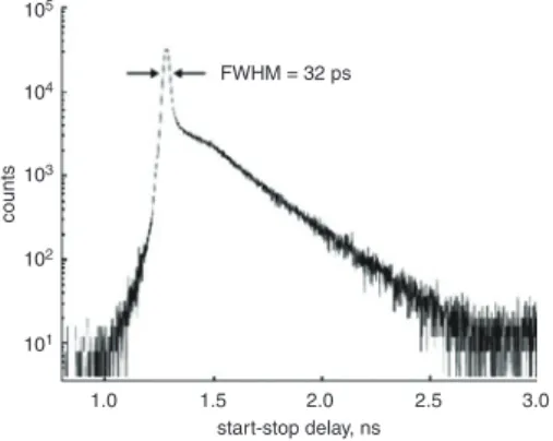
A simple circuit on the PCB translates the front-end output into a nuclear instrumentation module (NIM) standard signal to be fed to the following electronics. The SPAD was illuminated with a laser diode (Antel MPL-820 laser module) emitting optical pulses at 820 nm with about 10 ps FWHM. The instrument response function (IRF) was acquired with a commercial time-correlated single photon counting module (Becker&Hickl SPC-130) by applying the NIM signal generated by the front-end circuit to the START input and the synchronous, trigger-out electrical signal provided by the laser to the STOP input. Biasing the detector 5 V above its breakdown voltage and using VDD,TIAequal to 1.8 V and VTH equal to 1.6 V (corresponding to an equivalent threshold of 200 mV) we obtained the IRF reported in Fig.3featuring a timing jitter as low as 32 ps FWHM. To the best of our knowledge, this is the lowest timing jitter ever reported in literature with a fully inte-grated circuit and a custom technology SPAD detector.
105 104 103 102 101 1.0 FWHM = 32 ps 1.5 2.0 2.5 3.0 start-stop delay, ns counts
Fig. 3 IRF of designed front-end circuit with a 50 µm-diameter custom tech-nology SPAD biased at 5 V of excess bias
transimpedance amplifier
output driver
compar
ator
Fig. 4 Layout of designed front end circuit
Table 1: Measurement of the timing jitter of a 50 µm-diameter custom technology SPAD biased at 5 V of overvoltage with the designed front-end circuit
VTH(mV) Timing Jitter FWHM (ps)
200 32
400 47
600 48.5
800 49
Concerning VDD,TIA, it was observed that this bias voltage does not influence significantly the timing jitter as long as it is greater than 1.4 V; otherwise the output stage MOSFET M6 (see Fig. 1) is too close to ohmic regime and this has to be avoided in order to have a sharp signal to be fed to the following comparator. In this range, we
decided to set VDD,TIA equal to 1.8 V because this value will allow us to reduce the number of required bonding pads, being this a very impor-tant issue in future developments of a densely integrated system.
Table 1 reports the timing jitter as a function of VTH. As expected, the timing jitter increases when VTH is increased due to the dependence of the SPAD intrinsic jitter on the equivalent current threshold used to determine the onset of the avalanche current [5]. It is worth noting that the designed circuit not only provides state-of-art timing accuracy with a threshold much higher than previously reported works (i.e. 200 mV instead of 8 mV used in [6]), but it can be also used with a threshold of several hundreds of millivolts still providing a timing precision better than 50 ps. The layout of the circuit without bonding pads is shown in Fig. 4: it features an area occupation equal
to 11013 µm2 and the power dissipation of the front end excluding the output driver is as low as 1.3 mW. These results make the integrated front end circuit presented here a valuable building block of a high per-formance timing system based on SPAD arrays.
Conclusions: Photon timing measurements with SPAD arrays are widely used in many applications. The development of densely integrated high performance detection systems, though, has been limited so far by the lack of front end circuits able to extract the timing information with a jitter of few tens of picoseconds and suitable to be exploited in large arrays. In this Letter, we have presented the first fully integrated circuit capable to extract the timing information from custom technology SPAD detectors with a jitter as low as 32 ps. Thanks to a low power dis-sipation and area occupation, the circuit can be a valuable building block of detection system based on SPAD arrays.
G. Acconcia, I. Rech, I. Labanca and M. Ghioni (DEIB, Politecnico di Milano, piazza L. Da Vinci 32, 20133, Milan, Italy)
✉ E-mail: [email protected] References
1 Becker, W.: ‘Advanced time-correlated single photon counting applications’ (Springer International Publishing, Switzerland, 2015) 2 Gordon, K.J., Fernandez, V., Buller, G.S., Rech, I., Cova, S.D., and
Townsend, P.D.:‘Quantum key distribution system clocked at 2 GHz’, Optics Express, 2005, 13, (8), pp. 3015–3020, doi: 10.1364/ OPEX.13.003015
3 McCarthy, A., Ren, X., Della Frera, A., et al.:‘Kilometer-range depth imaging at 1550 nm wavelength using an InGaAs/InP single-photon ava-lanche diode detector’, Optics Express, 2013, 21, (19), pp. 22098–22113, doi: 10.1364/OE.21.022098
4 Bronzi, D., Villa, F., Tisa, S., Tosi, A., and Zappa, F.:‘SPAD Figures of merit for photon-counting, photon-timing, and imaging applications: A review’, IEEE Sens. J., 2016, 16, (1), pp. 3–12, doi: 10.1109/ JSEN.2015.2483565
5 Ghioni, M., Gulinatti, A., Rech, I., Maccagnani, P., and Cova, S.: ‘Large-area low-jitter silicon single photon avalanche diodes’. Integrated Optoelectronic Devices, San Jose, USA, February 2008, pp. 69001D–69001D, doi: 10.1117/12.761578
6 Gulinatti, A., Maccagnani, P., Rech, I., Ghioni, M., and Cova, S.:‘35 ps time resolution at room temperature with large area single photon ava-lanche diodes’, Electron. Lett., 2005, 41, (5), pp. 272–274, doi: 10.1049/el:20047445
7 Crotti, M., Rech, I., Gulinatti, A., and Ghioni, M.:‘Avalanche current read-out circuit for low-jitter parallel photon timing’, Electron. Lett., 2013, 49, (16), pp. 1017–1018, doi: 10.1049/el.2013.1879
8 Crotti, M., Rech, I., Acconcia, G., Gulinatti, A., and Ghioni, M.:‘A 2-GHz bandwidth, integrated transimpedance amplifier for single-photon timing applications’, IEEE Trans. Very Large Scale Integr. (VLSI) Syst., 2015, 23, (12), pp. 2819–2828, doi: 10.1109/TVLSI.2014.2382551