Porous versus Compact Nanosized Fe(III)-Based Water Oxidation
Catalyst for Photoanodes Functionalization
Michele Orlandi,
*
,†Nicola Dalle Carbonare,
‡Stefano Caramori,
‡Carlo A. Bignozzi,
‡Serena Berardi,
‡Alberto Mazzi,
†Zakaria El Koura,
†Nicola Bazzanella,
†Nainesh Patel,
§and Antonio Miotello
††Department of Physics, University of Trento, I-38123, Povo, Trento, Italy
‡Department of Chemical and Pharmaceutical Sciences, University of Ferrara, Via Fossato di Mortara 17-19, 44100 Ferrara, Italy §Department of Physics, University of Mumbai, Vidyanagari, Santacruz (E), Mumbai 400 098, India
*
S Supporting InformationABSTRACT: Integrated absorber/electrocatalyst schemes are increasingly adopted in the design of photoelectrodes for photoelectrochemical cells because they can take advantage of separately optimized components. Such schemes also lead to the emergence of novel challenges, among which parasitic light absorption and the nature of the absorber/catalyst junction features prominently. By taking advantage of the versatility of pulsed-laser deposition technique, we fabricated a porous iron(III) oxide nanoparticle-assembled coating that is both transparent to visible light and active as an electrocatalyst for water oxidation. Compared to a compact morphology, the
porous catalyst used to functionalize crystalline hematite photoanodes exhibits a superior photoresponse, resulting in a drastic lowering of the photocurrent overpotential (about 200 mV) and a concomitant 5-fold increase in photocurrents at 1.23 V versus reversible hydrogen electrode. Photoelectrochemical impedance spectroscopy indicated a large increase in trapped surface hole capacitance coupled with a decreased charge transfer resistance, consistent with the possible formation of an adaptive junction between the absorber and the porous nanostructured catalyst. The observed effect is among the most prominent reported for the coupling of an electrocatalyst with a thin layer absorber.
KEYWORDS: pulsed-laser deposition, a-Fe2O3, water splitting, photoanodes, hematite, adaptive junction, nanostructures
■
INTRODUCTIONMaterials designed for photodriven fuel synthesis must perform two essential functions: (1) sunlight absorption to generate electron−hole pairs and (2) catalysis of the fuel-forming reactions. The latter becomes critical when multielectron redox reactions are involved, leading to slow kinetics and consequent loss of efficiency. A significant example is photochemical water electrolysis performed in a photoelectrochemical cell (PEC), where the strict kinetic requirements dictated in particular by the oxygen evolution reaction, which involves the proton-coupled exchange of four electrons, have driven for decades the search for efficient catalysts.1−3
In recent years, the research efforts have been increasingly directed toward schemes where the two functions are separately optimized and then integrated by functionalization of absorber materials with redox catalysts. Examples include inorganic semiconductors or molecular chromophores as absorbers, functionalized by coupling with molecular catalysts or nanostructures of metals or metal oxides.4−11 This kind of scheme allows for a simpler yet more in-depth screening of candidate catalysts while taking advantage of materials with already optimized optical properties (e.g., for photovoltaic applications) but also presents new challenges. Two critical
issues are (a) the nature of the absorber/catalyst junction and (b) the parasitic light blocking5,12by catalysts deposited on the absorber surface. The former depends largely on the morphology of the catalyst, with dense ion-impermeable structures yielding buried junctions and nonoptimal perform-ance. By contrast, porous ion-permeable architectures can lead to adaptive junctions and substantially enhanced charge separation and photovoltage generation.13As for the latter, in the case of metal oxides oxygen evolving catalysts (OEC) deposited on photoanodes, the effect of optical losses on the overall efficiency is so severe that in a recent investigation the best performance was obtained with a subnanometric film thickness.14However, a higher catalyst mass loading is generally beneficial to reduce overpotential. This trade-off between optical losses and catalyst loading limits the application of earth-abundant, cheap, and scalable alternatives to noble-metal-based catalysts because the replacements generally have lower catalytic activity and higher quantities would be needed to produce a comparable performance.15,16
Received: April 29, 2016 Accepted: July 22, 2016 Published: July 22, 2016
Research Article
www.acsami.org
© 2016 American Chemical Society 20003 DOI:10.1021/acsami.6b05135 copying and redistribution of the article or any adaptations for non-commercial purposes.
on laser ablation of a target material, we were able to perform a comparative investigation where by changing the deposition conditions different morphologies of a catalytic material having the same nominal composition (i.e., a largely amorphous iron(III) oxide), ranging from a dense compact layer to a porous nanoparticle-assembled coating, were cast on nano-crystalline hematite thin layers (HTL) acting as light absorber. The latter was selected as model host substrate by virtue of their ease of fabrication with good reproducibility and acceptable baseline performances in photoelectrochemical water oxidation arising from their thickness (ca. 30 nm), which not only yields modest light-harvesting capability but also is compatible with the short carrier diffusion lengths of hematite.18The photoresponse of these modified photoanodes, consisting of the integrated absorber-catalyst system, was largely affected by the specific nature of the catalytic layer. The densefilm deposition invariably leads to a large decrease in the photoelectrochemical response with respect to the unmodified film, and photoanodes decorated with the porous catalyst show a drastic lowering of the photocurrent over-potential (about 200 mV) and a concomitant 5-fold increase in photocurrents at 1.23 V versus reversible hydrogen electrode (vs RHE) in 0.1 M NaOH (pH 13.3). This provides an additional guideline, besides the evaluation of the “dark” electrochemical activity of the oxygen evolving species, on the properties that should be pursued for the successful integration of a charge transfer catalyst in a photoelectrode for water splitting. Clearly, the choice of iron oxide as both the absorber material and OEC is motivated by the need to find earth-abundant, cheap, and scalable materials to enable the large-scale application of solar water-splitting schemes. Iron oxide not only satisfies all these requisites19 but also is nontoxic and environmentally safe.
■
EXPERIMENTAL METHODSMaterials. FeCl3·6H2O (≥99%) and NaOH (98%) were purchased
from Alfa Aesar. Polyethylene glycol bisphenol A epichlorohydrin copolymer (mol wt 15 000−20 000 Da) were purchased from Sigma-Aldrich. Fluorine-doped tin oxide glass slides (FTO, TEC 8Ω/cm2,
Hartford Glass) were cleaned by successive 30 min ultrasonic treatments in acetone, ethanol, aqueous Alconox (Sigma-Aldrich) solution, and distilled water and then blown dry with a warm air stream. A portion of the slides was then masked with KAPTON tape (Tesa) to preserve an uncovered zone for the electric contact. A metallic iron disc (purity 99.9%, Sematrade) was used as the target material for PLD.
Crystalline Hematite Thin Layers (HTL) Preparation. FeCl3·6H2O
(0.54 g) was dissolved in DI water (20 mL), and then polyethylene glycol bisphenol A epichlorohydrin copolymer (0.54 g) was added under gentle stirring to avoid the formation of bubbles. The solution was spin-coated onto FTO glass (1000 rpm for 9 s and 2000 rpm for 30 s). After each spin-coated cycle the glass slide was annealed at 550 °C for 15 min in air. Spin-coating cycles were repeated 3 times, and after the third cycle, the electrode was heated at 550°C for 2 h and
Deposition was performed at a constant oxygen pressure of 45 Pa. The distance between the metallic iron target and substrates was set to 5.5 cm and the number of pulses wasfixed (2000 pulses), to ensure that all samples have the same quantity of material. Substrate temperatures were either RT or 300°C (DEP300). A more detailed description of the PLD apparatus is available elsewhere.20 For comparison, some samples were deposited at RT and then annealed at 300 and 550°C in air in a tubular furnace. These are labeled AN300 and AN550 respectively. The heating rate was set to 10°C/min, and the desired temperature was kept constant for 2 h.
Characterization. Scanning electron microscopy (SEM) was used to analyze the morphology and the thickness of the films. Measurements were performed using a JEOL JSM-7001F FEG-SEM at 20.0 keV electron beam energy. The SEM apparatus is equipped with an energy dispersive X-ray spectroscopy detector (EDXS, Oxford INCA PentaFETx3). The working distance was maintained between 3 and 8 mm. Surface morphology images were acquired in top-down and tilted modes, whereas cross-sectional analysis was performed putting thefilms on a 90° stub.
Raman measurements were performed on a Horiba LabAramis setup equipped with a HeNe 633 nm laser as source and a confocal microscope (100× objective) coupled to a 460 mm focal length CCD-based spectrograph equipped with a four interchangeable gratings turret. In the range between 450 and 850 nm, the wavenumber accuracy is 1 cm−1with a 1800 L/mm grating. The laser power is 15 mW, and the maximum spot size is 5μm. An accumulation number of 10 and an exposure time of 7 s were employed for all measurements. UV−vis absorption was studied using a Varian Cary 5000 spectrophotometer, and quartz substrate was also used to investigate the UV region.
Stationary emission spectra were measured with an Edinburgh Instruments FLS 920 spectrofluorimeter, equipped with a double emission monochromator by using an excitation bandwidth (Δλ) of 7 nm. The ferric oxide thinfilms (RT, AN300, and DEP300) deposited on quartz slides were placed in a dedicatedfilm holder equipped with a micrometer stage in order to optimize the angle between the thinfilm, the excitation beam and the emitted light reaching the detector. The S/N ratio was optimized by summing 10 subsequent scans with 1 nm wavelength step and a dwell time of 0.1 s. Spectra were corrected for the photomultiplier (R928P-Hamamatsu) response by using a factory-built calibrationfile. Excitation was in the absorption manifold of the ferric oxide, either at 350 or 300 nm. Two different types of cutoff filters (395 and 350 nm) prevented scattered excitation light from reaching the phototubes.
XPS was performed using a PHI 5000 VersaProbe II equipped with a monochromatic Al Kα (1486.6 eV) X-ray source and a hemispherical analyzer. Electrical charge compensation was required to perform the XPS analysis. The sample surface was sputtered for 30 s in order to remove any surface oxidation.
J−V and constant potential electrolysis experiments were carried out in a three-electrode configuration cell using a platinum electrode and a saturated calomel electrode (SCE) as counter and reference electrodes, respectively. The cell containing aqueous NaOH (either 0.1 M, pH 13.3, or 1 M, pH 14) as electrolyte was connected to an Eco Chemie Autolab PGSTAT 302/N electrochemical work-station. J−V curves were recorded at a scan speed of 20 mV s−1. For the measurements under illumination, the working electrode was
DOI:10.1021/acsami.6b05135
irradiated using an ABET solar simulator (AM 1.5G, 100 mW cm−2), and the illuminated area was 1 cm2.
IPCE spectra were recorded under a potential bias of both 1.1 and 1.5 V vs RHE. The steady-state photoanodic current was recorded every 10 nm from 330 and 600 nm on a PGSTAT 30 electrochemical workstation. The incident monochromatic irradiance was measured with a calibrated silicon photodiode (Centronic ASD100−7Q). IPCE was calculated according to
λ = × λ μ λ − − − J P IPCE 1.24 10 (Vm) ( A cm ) (nm) (Wm ) 3 2 2
where Jλis the photocurrent density at the wavelengthλ and Pλis the
incident radiant power. APCE was obtained according to IPCE/LHE, where LHE(λ) = (1−10−A(λ)) and A is the absorbance of the photoelectrode measured in transmission mode taken from the electronic spectra reported inFigure S5.
Dissolved oxygen evolved during (photo)electrochemical experi-ments with HTL-AN300 and AN300 was measured in a sealed cell under nitrogen atmosphere by using a polarographic sensor (Crison Oxi 45+) calibrated in air-saturated water by following a single point procedure. Comparative O2 evolution experiments were carried out
under galvanostatic conditions (using the same current as that observed with the Fe-based thinfilms) by using IrO2/FTO working
electrode obtained by spin-casting colloidal IrO2 nanoparticles
fabricated according to Hara et al.21
Potentiostatic impedance data of photoanodes under illumination were recorded in the three-electrode configuration cell described above in 0.1 M NaOH (pH 13.3). Sample data were obtained from −0.73 to 1.53 V vs RHE at 50 mV intervals employing a FRA2.v10 frequency-response analyzer controlled by Nova 1.10. A 10 mV amplitude sinusoidal perturbation (single sine) whose frequency ranged between 100 000 and 0.05 Hz was adopted. The impedance response wasfitted using ZView software with the electric equivalent reported inFigure S9.
■
RESULTS AND DISCUSSIONCross-sectional SEM analysis of RT samples deposited on silicon substrates reveals a complex morphology with scattered particles of diameter in the range of about 30−300 nm covered by a porous structure made of smaller particles assembled in irregular wires (Figures 1a and S1 for lower magnification images). As the size of these latter particles approaches the spatial resolution of the SEM apparatus (2 nm), a conservative estimation for their average diameter is 5± 2 nm. Because of the very rough morphology, it is not possible to define a layer thickness, but the surface coverage appears to be complete (Figure 1c). Annealing of RT samples at 300°C results in a Figure 1.SEM analysis of (a and c) RT, (d) AN300, (e) AN550 and (b and f) DEP300. Substrate is silicon for all samples.
ACS Applied Materials & Interfaces
DOI:10.1021/acsami.6b05135
the oxygen atmosphere reduces the kinetic energy of the ablated material, limits the plume expansion, and promotes collisions between ablated particles. This results in the formation of nanoclusters in the plume, which are cooled down by the background gas before reaching the substrate where they create a porous structure. By contrast, in lower pressure conditions, the plume expansion is less confined, the ablated material retains an higher kinetic energy, and the higher mobility allows aggregation of the particles after deposition on the substrate. The result is a more dense microstructure composed of partially fused NPs.23,24
Raman analysis (Figure 2) reveals the presence of the crystalline hematite main peaks25at 226 and 292 cm−1only in
the case of the sample annealed at 550°C. All other samples show spectra with features not clearly different from the FTO reference. This is an indication of the largely amorphous nature of the deposited material, which is known to yield better OER catalysis performance than the crystalline phase.26
XPS analysis confirms that the only oxidation state of iron is Fe(III) (Fe 2p1/2peak BE = 710.2± 0.5 eV and Fe 2p3/2peak BE = 723.7± 0.5 eV; seeFigure S2) in all samples.
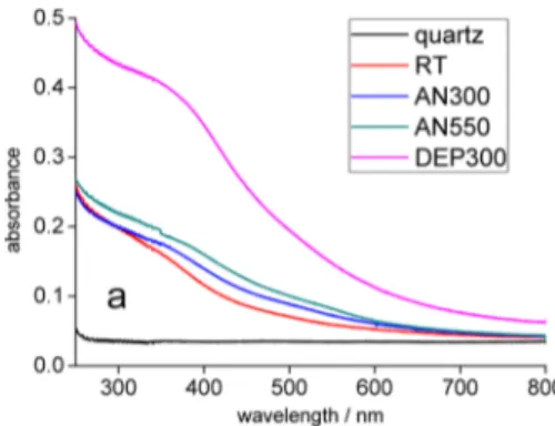
From the analysis of UV−vis absorption spectra on quartz substrates (Figure 3), two important observations emerge: (i) The sample DEP300 shows a much higher absorbance in all the investigated range. (ii) The absorbance correlates with
morphology in the direction of higher values for more compact films.
In the PLD methodology, the quantity of deposited material depends essentially on (a) the ablation rate, (b) the background gas pressure that determines the plume expansion, (c) the target-to-substrate distance, and (d) the number of laser pulses. In our case, a−c are kept constant, and only the number of pulses is varied. The ablation rate depends on the laserfluency (J/cm2), which is constant, and on the target morphology, which is altered by the ablation process. In our system, this effect is minimized by a pattern of target motion designed to ensure homogeneous erosion of the target surface.20In other reports by our group, where the quantity of catalyst involved is higher, the relation between number of pulses and deposited material has been verified by weighing the substrates before and after the deposition.27,28 In other papers where thin-films morphologies were investigated, we verified a reproducible relation between film thickness (and hence the quantity of material deposited) and number of pulses.22,29
Given that the quantity of deposited material at a given pressure is essentially set by the number of pulses, which is kept constant for all depositions, the difference between RT and DEP300 is all the more striking. The reason for this behavior probably lies in the different morphology of the films. DEP300 is essentially a bidimensional thin-film, although with a nanostructured surface, whereas RT exhibits a tridimensional architecture with scattered big particles and a substantial fraction of the surface composed of very small particles (5± 2 nm). In this latter case, a reasonable hypothesis is that a size effect in the form of optical quantum confinement dominates the optical properties, as reported for other materials30and for other nanosized hematites.31,32 A recent investigation17 observed a remarkable blueshift of up to 0.3 eV for both direct and indirect transitions when decreasing a hematite film thickness from 20 to 4 nm, leading to an high degree of transparency in the visible region. The effect is size-dependent and ascribed by the authors to quantum confinement. It should be however recalled that also a small change in the refractive index of the catalyticfilm could lead to enhanced transparency. Nevertheless, the observation of a well-defined emission band at ca. 450 nm, consistent with the band gap of the RT and AN300 thinfilms, is suggestive of the presence and possibly of the coexistence of quantum−optical phenomena (Figure S6). Such a feature appears to characterize only the RT and AN300 samples and is lost in the AN550 and DEP300 thin films in agreement with the collapse of the nanostructures observed by SEM micrography. Reducing hematite particle diameter to the 5± 2 nm level could help alleviate the problem of a very short hole-diffusion length, lying in the nanometer range,33but the Figure 2.Raman spectra on FTO substrates.
Figure 3.UV−vis absorption spectra on quartz substrates.
DOI:10.1021/acsami.6b05135
resulting low absorption is an issue in the design of photoactive devices based on a single material. This effect can instead be exploited to functionalize an absorber with a transparent iron oxide OER catalyst.
Fe2O3 is stable in alkaline environment (pH >9.8), so
electrochemical water oxidation experiments were performed at pH 14 (1 M NaOH) to ensure a well-defined electrochemistry. The oxygen evolution is expected at potential more positive than 1.23 V vs RHE.Figure 4a illustrates the current responses of the amorphous iron oxidefilms cast on FTO along with that of a bare FTO taken as a reference.
The linear scan reveals that all samples are active toward water oxidation, with both DEP300 and AN300 showing considerable electroactivity with overpotentials (taken at current density J = 0.2 mA cm−2) of 408 and 433 mV, respectively. However, the current response of RT decreased
considerably during a constant potential electrolysis experiment at 1.83 V vs RHE, designed to test film stability under operational conditions at moderate current densities (Figure 4b). The current density loss for RT is of 44%, whereas DEP300 is substantially stable with only a 6% loss. AN300 and AN550 show an intermediate stability with a relative decrease of 10−11%. In the case of RT, the performance degradation is irreversible and is due to detachment of active material, as observed by SEM images taken after prolonged electrolysis (Figure S3). Conversely, the initial performance of AN300 was reobserved on successive J−V scans (Figure S4) after restoring the electrode by abundant rinsing with water and heating at 80 °C in air for 2 h. In this case, the current decrease during electrolysis may originate by adsorption of molecular oxygen, ions, and oxidation intermediates, limiting the active surface of the electrode, rather than by mechanical detachment of a-Figure 4.(a) Linear sweep voltammetry on FTO substrates and (b) chronoamperometry at 1.83 V vs RHE.
Figure 5.(a) J−V curves of HTL, HTL-AN300, and HTL-DEP300 recorded under AM 1.5 G illumination (100 mW cm−2) and in the dark in 0.1 M NaOH (pH 13.3). (b) IPCE spectra of the same samples recorded at 1.5 V vs RHE shining the electrodes from both the back (full symbols) and front side (empty symbols). (c) APCE spectra of the photoelectrodes reported in panel b. (d) Oxygen evolution in 0.1 M NaOH (pH 13.3) observed during constant potential photoelectrolysis with HTL-AN300 (AM 1.5 G, 100 mW cm−2) held at 1.52 V vs RHE (black squares) compared to the dark electrolysis with an IrO2/FTO electrode (red circles) biased at the same current (0.48 mA) of the hematite based photoelectrode.
ACS Applied Materials & Interfaces
DOI:10.1021/acsami.6b05135
Fe2O3. From a purely electrocatalytic point of view, DEP300 is
the best electrode, with J = 41.2 mA cm−2at 2.53 V vs RHE, whereas AN550 is limited to 36 mA cm−2at the same potential value, confirming that the amorphous material is a better catalyst than crystalline hematite, as reported by recent literature.26,34 To verify the application of these iron-based catalysts in photocatalytic devices, HTL electrodes prepared by spin-coating have been functionalized by PLD with AN300 and DEP300 iron-based structures (indicated as HTL-AN300 and HTL-DEP300). The current−voltage behavior of the modified HTLs, recorded by scanning the photoelectrodes under AM 1.5G illumination (at 100 mW cm−2simulated sunlight) in 0.1
M NaOH (pH 13.3), reveals a significantly improved
photoelectrode performance after the functionalization with AN300 (Figure 5a). The photocurrent improves along the whole potential region of interest, reaching 0.4 mA cm−2at 1.23 V vs RHE with respect to ca. 0.08 mA cm−2for the unmodified HTL at the same potential. The curve of HTL-AN300 also shows a cathodic shift of the photocurrent onset of about 200 mV (ca. 0.9 V vs RHE for HTL-AN300 with respect to 1.1 V vs RHE observed for the bare HTLfilm) representing, so far, one of the most prominent OEC-induced decreases in photoanodic overpotential.35,36 Differently, the functionalization of HTL with the more compact DEP300 has an adverse effect on the photocurrent generation. The“dark” catalytic effect of DEP300 is evident from the rising of the anodic discharge starting at ca. 1.6 V vs RHE, but the photocurrent generated at lower applied bias is largely inferior to that observed with the unmodified HTL, suggesting a significant degree of recombination or the blocking of the hole transfer from the underlying HTL, where photocharge is generated, to the electrolyte. IPCE spectra recorded at 1.5 V vs RHE are consistent with the J−V response discussed above, showing better charge generation and transfer properties for the AN300 modified photoelectrode (Figure 5b). Given the nanometer thicknesses of the photoelectrode and of the catalytic overlayer, no large differences were observed by changing the illumination mode from back (contact side) to front (electrolyte side), in agreement with the absorption profile of both the unmodified and modified samples (Figure S5), ruling out a parasitic effect of the catalysts on the absorption capability of the semiconductor. IPCE spectra collected in back and front mode are indeed nearly super-imposable, with only a slight improvement in the absolute values of photon to electron conversion observed in back illumination mode, consistent with the shorter electron collection path. The photoaction spectra of HTL-AN300 recorded at 1.1 V vs RHE (Figure S7), where no photocurrent
is detected for the unmodified HTL sample, display the same shape of the IPCE spectra recorded at 1.5 V vs RHE for both HTL and HTL-AN300, suggesting that the charge generation involves essentially the underlying crystalline hematite and that the AN300 catalyst improves the photoresponse of the combined electrode by participating essentially to the secondary hole scavenging events that follow the primary charge generation within the crystalline hematite film. APCE spectra (Figure 5c) corroborate the piece of evidence gained from the IPCE measurements, showing that the HTL-AN300 photoelectrode is intrinsically able to generate and separate photocharge with an efficiency which is at least twice that of the unmodified HTL.
Amperometric oxygen measurements in solution confirm that both the AN300 catalyst (Figure S8) and HTL-AN300 (Figure 5d) are able to evolve oxygen at a rate which is comparable to that of a transparent IrO2/FTO electrode biased at the same anodic current.
Electrochemical impedance spectroscopy (EIS) data allowed us to obtain more precise information about the nature of the charge transfer processes and were interpreted with the simplified equivalent circuit reported in previous contribu-tions18,37,38 and in Figure S9, comprising a nested mesh describing both the charge transfer across the depletion layer (R2-CPE1) and the Helmholtz layer (R3-CPE2). The charge transfer resistance (R3) associated with the trapping of holes in surface states is the dominating resistive component in the interfacial dynamics of these type of hematite photoelectrodes, describing well the J−V characteristic for both unmodified and AN300 modified films (Figure S10). The capacitance associated with such resistance (CPE2) follows in both HTL and HTL-AN300 a bell-shaped distribution typical of the trapping of photoholes in surface states (Figure 6a), leading to the generation of highly valent reactive states responsible for the formation of Fe(IV)O type reactive species, which are considered thefirst key intermediates for the oxygen evolution reaction.39 The trapped photohole capacitance undergoes indeed a negative shift and a significant enhancement in the presence of the porous AN300 catalyst (1.56× 10⁻⁵and 4.56× 10⁻⁵ F for the integrated values of HTL and HTL-AN300 respectively), justifying the improved performances of the latter. The formation of oxidized catalyst states in the porous layer must be compensated by the exchange of ions (namely, OH− and H+/Na+) with the electrolyte probably resulting in
the formation of an adaptive junction with the semi-conductor,13 where the Fermi level of the photoactive semiconductor is essentially unpinned from that of the Figure 6.(a) CPE2 and (b) R3 plot of HTL, HTL-AN300, and HTL-DEP300 recorded under AM 1.5G illumination in 0.1 M NaOH (pH 13.3). The dotted vertical bar in the graphs indicates the thermodynamic potential of water oxidation.
DOI:10.1021/acsami.6b05135
amorphous catalyst present in the form of highly nano-structured or discontinuous islands. At present, our attempts to establish an ohmic contact with the catalyst by evaporating a gold contact in order to independently probe its Fermi level, as described in ref13, failed due to electrical shorting. This may be due to the exceedingly thin active layers and to the porous morphology of the outer catalytic layer resulting in the direct contact of gold with either the crystalline semiconductor or FTO. Nevertheless, the trapping of holes corresponding to formation and stabilization of Fe(IV) species, revealed clearly by EIS, should automatically imply a variation of the Fermi level of the catalyst that is able to move independently from that of the semiconductor. APCE spectra (Figure 5c) rule out a role of light absorption in explaining the improved performance of the HTL-AN300, consistent with EIS result being able to separate photocharge with a maximum internal efficiency that is about twice that of the unmodified HTL. It should be noted that the charge transfer resistance shows a broad minimum correspondening to the capacitance maximum of the HTL-AN300 (Figure 6b), corroborating the correlation between improved surface trap capacitance and reduced charge transfer resistance of the interface. By contrast, the compact catalytic film (DEP300) is seemingly unable to trap holes, with the interfacial capacitance being essentially constant and at low values (ca. 3.5 × 10⁻⁵ F cm−2) within the whole potential interval where photocurrent is observed, only showing a sizable increase at potentials corresponding to the dark anodic discharge (Figure 6a) where the Fermi level under potentio-static control intercepts directly the electrochemically active sites of the DEP300 film. The reduced performance of the compact modified HTL-DEP300 junction might be due to both the compact morphology of DEP300, offering a smaller number of reactive sites where photoholes could trap, and to the lower permeability of this compact layer to the electrolyte, which does not allow charge to compensate as easily as in the AN300 layer the trapping of photoholes with the movement of anions to and from the electrolyte. Consistent with such hypothesis, the charge transfer resistance is significantly higher than that in both HTL and HTL-AN300 (Figure 6b), steadily decreasing in an almost linear fashion with the increasing potential, instead of sharply dropping as observed in the latter cases.
Finally, the 100 Hz Mott−Schottky plots show a linear behavior of the 1/C2 versus applied potential, in agreement
with the formation of a depletion layer (Figure 7a). The donor density (ca. 3 × 1017 cm−3) for the HTL and HTL-AN300
agree with previously found values for similar type of electrodes
fabricated by our groups.18 By contrast, although the HTL-DEP300 shows a linear behavior as well, a 10-fold increased donor density (2 × 1018 cm−3) is found, suggesting that the depletion layer may extend into the amorphous compact layer having a larger number of defects which contribute to boosting the overall donor density. This effect could be useful to improve the overall n-type conductivity of the thinfilms; the resistance associated with the depletion layer (R2) is indeed smaller in the HTL-DEP300 with respect to the other two electrode types (Figure 7b) but will be quite irrelevant in determining the performance of combined films having an overall thickness of less than 50 nm. Most importantly, the involvement of the space charge layer within the DEP300 is consistent with the fact that Fermi level variations within the catalytic DEP300 film occur by acting on the width of the depletion layer rather than by charge compensation with the electrolyte and that the Fermi levels of the crystalline photoelectrode and of the catalyst are not able to move independently of each other. Photoholes will thus have to travel from the crystalline layer through the defective amorphous DEP300 layer, being exposed to recombination reactions, before reaching the interface with the electrolyte where scavenging, leading to oxygen evolution, could finally occur. This explains the lack of a distinct hole-trapping capacitance peak as well as the low capacitance values and the high charge transfer resistance, consistent with DEP300 behaving, in practice, as an intermediate hole-blocking interface, resulting in a large decrease of the photocurrent with respect of that of the unmodified sample. Only the dark electrochemical discharge will be evident in the combined HTL-DEP300 electrode, as indeed experimentally observed, when the applied potential, moving further to anodic values, directly intercepts the redox active sites of the catalyst.
■
CONCLUSIONSPLD, an easily scalable fabrication technique already applied in a variety of industrial processes,40 proves to be a versatile method to control morphology at the nanometric scale, thus allowing a systematic investigation of morphological and electronic effects on the properties of functional materials. In this work we have designed and synthesized by PLD a porous amorphous Fe2O3 OEC based on a nanoparticle-assembled coating morphology. This coating is found to be highly transparent in the visible range possibly due to a quantum confinement effect induced by the size of the nanostructures in the order of few nanometers and to retain the previously Figure 7.(a) Mott−Schottky plot recorded at 100 Hz under AM 1.5 illumination in 0.1 M NaOH (pH 13.3) for HTL, AN300, and HTL-DEP300. (b) R2 plot of the same samples.
ACS Applied Materials & Interfaces
DOI:10.1021/acsami.6b05135
functionalization of the hematite photoanodes with a more compact catalyst morphology, exhibiting better electrocatalytic properties, is detrimental to photocurrent generation. In our case, J−V curves under illumination, IPCE analysis, and EIS point to the nature of the absorber/catalyst junction rather than to the parasitic light blocking as the dominant factor in determining the PEC performance. Indeed, APCE and EIS data are consistent with a much better charge separation in the porous morphology that may stem from the formation of an adaptive junction allowing for the efficient storage of photogenerated holes within the porous catalyst. By contrast, the compact overlayer probably forms a buried junction, inhibiting hole transfer to the electrolyte. Regarding parasitic light absorption, while not critical in this case, likely due to the low thickness of the coatings (<20 nm for the compactfilm), the high transmittance, and solvent permeability of the porous morphology opens up the possibility of employing higher mass loadings of catalyst without loss of performance. This would be especially beneficial for earth-abundant, cheap, and scalable materials such as iron oxides.
Further work will be aimed at solving the stability problem of the most-transparent RT structures without resorting to the postdeposition thermal treatment by exploring deposition temperatures lower than 300 °C and at extending this methodology to more intrinsically active species such as bifunctional mixed-metal oxides.
■
ASSOCIATED CONTENT*
S Supporting InformationThe Supporting Information is available free of charge on the
ACS Publications websiteat DOI:10.1021/acsami.6b05135. Additional SEM images, XPS spectra, additional J−V curves, UV−vis spectra, emission spectra, IPCE spectra, oxygen evolution measurements under electrochemical conditions, and EIS data including the equivalent circuit used forfitting (PDF)
■
AUTHOR INFORMATIONCorresponding Author
*E-mail:[email protected]. Funding
The research activity is partially supported by the PAT (Provincia Autonoma di Trento) project ENAM in cooperation with Istituto MCB of CNR (Italy). FIRB Project Nanosolar (UNIFE) and the European Union’s Horizon 2020 Research and Innovation Programme under the Marie Skłodowska-Curie Grant Agreement No. 705723 (S.B.) is gratefully acknowledged for funding (UNIFE).
Notes
The authors declare no competingfinancial interest.
IPCE, incident photon-to-current efficiency APCE, absorbed photon-to-current efficiency
■
REFERENCES(1) Rüttinger, W.; Dismukes, G. C. Synthetic Water-Oxidation Catalysts for Artificial Photosynthetic Water Oxidation. Chem. Rev. 1997, 97, 1−24.
(2) Lewis, N. S. Light Work with Water. Nature 2001, 414, 589−590. (3) Kamat, P. V.; Bisquert, J. Solar Fuels. Photocatalytic Hydrogen Generation. J. Phys. Chem. C 2013, 117, 14873−14875.
(4) Youngblood, W. J.; Lee, S.-H. A.; Kobayashi, Y.; Hernandez-Pagan, E. A.; Hoertz, P. G.; Moore, T. A.; Moore, A. L.; Gust, D.; Mallouk, T. E. Photoassisted Overall Water Splitting in a Visible Light-Absorbing Dye-Sensitized Photoelectrochemical Cell. J. Am. Chem. Soc. 2009, 131, 926−927.
(5) Reece, S. Y.; Hamel, J. A.; Sung, K.; Jarvi, T. D.; Esswein, A. J.; Pijpers, J. J. H.; Nocera, D. G. Wireless Solar Water Splitting Using Silicon-Based Semiconductors and Earth-Abundant Catalysts. Science 2011, 334, 645−648.
(6) Cristino, V.; Berardi, S.; Caramori, S.; Argazzi, R.; Carli, S.; Meda, L.; Tacca, A.; Bignozzi, C. A. Efficient Solar Water Oxidation using Photovoltaic Devices Functionalized with Earth-abundant Oxygen Evolving Catalysts. Phys. Chem. Chem. Phys. 2013, 15, 13083−92.
(7) Orlandi, M.; Argazzi, R.; Sartorel, A.; Carraro, M.; Scorrano, G.; Bonchio, M.; Scandola, F. Ruthenium Polyoxometalate Water Splitting Catalyst: Very Fast Hole Scavenging from Photogenerated Oxidants. Chem. Commun. 2010, 46, 3152−4.
(8) Klahr, B.; Gimenez, S.; Fabregat-Santiago, F.; Bisquert, J.; Hamann, T. W. Photoelectrochemical and Impedance Spectroscopic Investigation of Water Oxidation with ″Co-Pi″-coated Hematite Electrodes. J. Am. Chem. Soc. 2012, 134, 16693−700.
(9) Sun, J.; Zhong, D. K.; Gamelin, D. R. Composite Photoanodes for Photoelectrochemical Solar Water Splitting. Energy Environ. Sci. 2010, 3, 1252−1261.
(10) Sartorel, A.; Bonchio, M.; Campagna, S.; Scandola, F. Tetrametallic Molecular Catalysts for Photochemical Water Oxidation. Chem. Soc. Rev. 2013, 42, 2262−2280.
(11) Ye, H.; Park, H. S.; Bard, A. J. Screening of Electrocatalysts for Photoelectrochemical Water Oxidation on W-Doped BiVO4 Photo-catalysts by Scanning Electrochemical Microscopy. J. Phys. Chem. C 2011, 115, 12464−12470.
(12) McKone, J. R.; Lewis, N. S.; Gray, H. B. Will Solar-Driven Water-Splitting Devices See the Light of Day? Chem. Mater. 2014, 26, 407−414.
(13) Lin, F.; Boettcher, S. W. Adaptive Semiconductor/Electro-catalyst Junctions in Water-Splitting Photoanodes. Nat. Mater. 2013, 13, 81−86.
(14) Trotochaud, L.; Mills, T. J.; Boettcher, S. W. An Optocatalytic Model for Semiconductor−Catalyst Water-Splitting Photoelectrodes Based on In Situ Optical Measurements on Operational Catalysts. J. Phys. Chem. Lett. 2013, 4, 931−935.
(15) Popczun, E. J.; McKone, J. R.; Read, C. G.; Biacchi, A. J.; Wiltrout, A. M.; Lewis, N. S.; Schaak, R. E. Nanostructured Nickel Phosphide as an Electrocatalyst for the Hydrogen Evolution Reaction. J. Am. Chem. Soc. 2013, 135, 9267−9270.
DOI:10.1021/acsami.6b05135
(16) McKone, J. R.; Sadtler, B. F.; Werlang, C. A.; Lewis, N. S.; Gray, H. B. Ni−Mo Nanopowders for Efficient Electrochemical Hydrogen Evolution. ACS Catal. 2013, 3, 166−169.
(17) Fondell, M.; Jacobsson, T. J.; Boman, M.; Edvinsson, T. Optical Quantum Confinement in Low Dimensional Hematite. J. Mater. Chem. A 2014, 2, 3352.
(18) Dalle Carbonare, N.; Carli, S.; Argazzi, R.; Orlandi, M.; Bazzanella, N.; Miotello, A.; Caramori, S.; Bignozzi, C. A. Improve-ment of the Electron Collection Efficiency in Porous Hematite Using a Thin Iron Oxide Underlayer: Towards Efficient All-Iron Based Photoelectrodes. Phys. Chem. Chem. Phys. 2015, 17, 29661−29670.
(19) Vesborg, P. C. K.; Jaramillo, T. F. Addressing the Terawatt Challenge: Scalability in the Supply of Chemical Elements for Renewable Energy. RSC Adv. 2012, 2, 7933.
(20) Bonelli, M.; Cestari, C.; Miotello, A. Pulsed Laser Deposition Apparatus for Applied Research. Meas. Sci. Technol. 1999, 10, 27.
(21) Hara, M.; Waraksa, C. C.; Lean, J. T.; Lewis, B. A.; Mallouk, T. E. Photocatalytic Water Oxidation in a Buffered Tris(2,2′-bipyridyl) ruthenium Complex-Colloidal IrO2 System. J. Phys. Chem. A 2000, 104, 5275−5280.
(22) Orlandi, M.; Caramori, S.; Ronconi, F.; Bignozzi, C. A.; El Koura, Z.; Bazzanella, N.; Meda, L.; Miotello, A. Pulsed-Laser Deposition of Nanostructured Iron Oxide Catalysts for Efficient Water Oxidation. ACS Appl. Mater. Interfaces 2014, 6, 6186−6190.
(23) Infortuna, A.; Harvey, A. S.; Gauckler, L. J. Microstructures of CGO and YSZ Thin Films by Pulsed Laser Deposition. Adv. Funct. Mater. 2008, 18, 127−135.
(24) Petrov, I.; Barna, P. B.; Hultman, L.; Greene, J. E. Microstructural Evolution During Film Growth. J. Vac. Sci. Technol., A 2003, 21, S117−S128.
(25) Jubb, A. M.; Allen, H. C. Vibrational Spectroscopic Character-ization of Hematite, Maghemite, and Magnetite Thin Films Produced by Vapor Deposition. ACS Appl. Mater. Interfaces 2010, 2, 2804−2812. (26) Smith, R. D.; Prevot, M. S.; Fagan, R. D.; Zhang, Z.; Sedach, P. A.; Siu, M. K.; Trudel, S.; Berlinguette, C. P. Photochemical Route for Accessing Amorphous Metal Oxide Materials for Water Oxidation Catalysis. Science 2013, 340, 60−3.
(27) Edla, R.; Patel, N.; Orlandi, M.; Bazzanella, N.; Bello, V.; Maurizio, C.; Mattei, G.; Mazzoldi, P.; Miotello, A. Highly Photo-Catalytically Active Hierarchical 3D Porous/Urchin Nanostructured Co3O4 Coating Synthesized by Pulsed Laser Deposition. Appl. Catal., B 2015, 166−167, 475−484.
(28) Patel, N.; Fernandes, R.; Guella, G.; Miotello, A. Nanoparticle-Assembled Co-B Thin Film for the Hydrolysis of Ammonia Borane: a Highly Active Catalyst for Hydrogen Production. Appl. Catal., B 2010, 95, 137−143.
(29) Schenato, M.; Ricardo, C. L. A.; Scardi, P.; Edla, R.; Miotello, A.; Orlandi, M.; Morrish, R. Effect of Annealing and Nanostructuring on Pulsed Laser Deposited WS2 for HER Catalysis. Appl. Catal., A 2016, 510, 156−160.
(30) Raymand, D.; Jacobsson, T. J.; Hermansson, K.; Edvinsson, T. Investigation of Vibrational Modes and Phonon Density of States in ZnO Quantum Dots. J. Phys. Chem. C 2012, 116, 6893−6901.
(31) Sivula, K.; Zboril, R.; Le Formal, F.; Robert, R.; Weidenkaff, A.; Tucek, J.; Frydrych, J.; Grätzel, M. Photoelectrochemical Water Splitting with Mesoporous Hematite Prepared by a Solution-Based Colloidal Approach. J. Am. Chem. Soc. 2010, 132, 7436−7444.
(32) Vayssieres, L.; Sathe, C.; Butorin, S. M.; Shuh, D. K.; Nordgren, J.; Guo, J. One-Dimensional Quantum-Confinement Effect in α-Fe2O3 Ultrafine Nanorod Arrays. Adv. Mater. 2005, 17, 2320−2323. (33) Klahr, B. M.; Martinson, A. B.; Hamann, T. W. Photo-electrochemical Investigation of Ultrathin Film Iron Oxide Solar Cells Prepared by Atomic Layer Deposition. Langmuir 2011, 27, 461−8.
(34) Smith, R. D.; Prevot, M. S.; Fagan, R. D.; Trudel, S.; Berlinguette, C. P. Water Oxidation Catalysis: Electrocatalytic Response to Metal Stoichiometry in Amorphous Metal Oxide Films Containing Iron, Cobalt, and Nickel. J. Am. Chem. Soc. 2013, 135, 11580−6.
(35) Tilley, S. D.; Cornuz, M.; Sivula, K.; Gratzel, M. Light-induced Water Splitting with Hematite: Improved Nanostructure and Iridium Oxide Catalysis. Angew. Chem., Int. Ed. 2010, 49, 6405−8.
(36) Young, K. M. H.; Hamann, T. W. Enhanced Photocatalytic Water Oxidation Efficiency with Ni(OH)2 Catalysts Deposited on α-Fe2O3 via ALD. Chem. Commun. 2014, 50, 8727−8730.
(37) Klahr, B.; Gimenez, S.; Fabregat-Santiago, F.; Hamann, T.; Bisquert, J. Water Oxidation at Hematite Photoelectrodes: The Role of Surface States. J. Am. Chem. Soc. 2012, 134, 4294−4302.
(38) Monllor-Satoca, D.; Bartsch, M.; Fabrega, C.; Genc, A.; Reinhard, S.; Andreu, T.; Arbiol, J.; Niederberger, M.; Morante, J. R. What Do You Do, Titanium? Insight Into the Role of Titanium Oxide as a Water Oxidation Promoter in Hematite-Based Photoanodes. Energy Environ. Sci. 2015, 8, 3242−3254.
(39) Klahr, B.; Gimenez, S.; Fabregat-Santiago, F.; Bisquert, J.; Hamann, T. W. Electrochemical and Photoelectrochemical Inves-tigation of Water Oxidation with Hematite Electrodes. Energy Environ. Sci. 2012, 5, 7626−7636.
(40) Gower, M. C. Industrial Applications of Laser Micromachining. Opt. Express 2000, 7, 56−67.
ACS Applied Materials & Interfaces
DOI:10.1021/acsami.6b05135