UNIVERSITY
OF TRENTO
DIPARTIMENTO DI INGEGNERIA E SCIENZA DELL’INFORMAZIONE 38123 Povo – Trento (Italy), Via Sommarive 14
http://www.disi.unitn.it
DETERMINATION OF THE COMPLEX PERMITTIVITY VALUES
OF PLANAR DIELECTRIC SUBSTRATES BYMEANS OF
AMULTIFREQUENCY PSO-BASED TECHNIQUE
R. Azaro, F. Caramanica, and G. Oliveri
January 2011
Determination of the Complex Permittivity Values of Planar
Dielectric Substrates by means of a Multifrequency PSO-based
Technique
R. Azaro, F. Caramanica, and G. Oliveri
ELEDIA Research Group
Department of Information Engineering and Computer Science University of Trento, Via Sommarive 14, 38050 Trento - Italy Tel. +39 0461 882057, Fax +39 0461 882093
Determination of the Complex Permittivity Values of Planar
Dielectric Substrates by means of a Multifrequency PSO-based
Technique
R. Azaro, F. Caramanica, and G. Oliveri
Abstract
In this paper, an innovative technique for the determination of the dielectric properties of planar substrates is presented. Starting from a set of impedance measurements per-formed on a section of a microstrip transmission line built on the planar dielectric substrate under test, the proposed technique formulates the reconstruction problem in terms of an optimization one successively solved by means of an effective stochastic algorithm. Such a method allows one the reconstruction of the permittivity values at multiple frequencies by simply using a vector network analyzer and a standard calibration procedure for the impedance measurement. The results of some representative experimental tests are shown for a preliminary assessment of the effectiveness of the proposed approach.
Key words:Permittivity Measurement, Dielectric Substrate Characterization, Microwave Mea-surements, Particle Swarm Optimizer.
1
Introduction
The knowledge of the dielectric properties of planar substrates is of great importance for an ef-fective design and development of planar antennas [1][2][3] and microwave circuits [4][5][6][7]. This is more important when dealing with low cost materials, whose performances are usually not guaranteed by the producers. Several methodologies have been developed in order to char-acterize dielectric materials in different frequency bands and with different accuracies. Some techniques are based on the use of resonant systems [10], while other techniques employ non-resonant sections of transmission lines [11][12]. Up to1 MHz, measurements setups are based
on lumped-component circuits, while distributed-parameter devices are employed when dealing with higher frequencies. In the latter case, the Material Under Test (MUT) is placed at the ter-minal section of a coaxial or waveguide transmission line, or inside a resonant cavity. Because of its simplicity and accuracy, the resonant cavity method [10], based on the detection of the resonant frequencies and losses, is widely used when homogeneous materials are considered. On the other hand, the transmission line method [11][12] determines the dielectric properties of the MUT by measuring amplitudes and phases of the signals transmitted and reflected by a material sample inserted in a transmission line. Other techniques devoted to the permittivity estimation in wide frequency bands are still derived from the transmission line method, but they are based on the use of open-ended and non-invasive coaxial probes [13][14]. Moreover, such techniques are generally used to characterize biological tissues [15]. Recently, an interesting method based on the use of a planar four-port microwave device and only-scalar measurements has been proposed in [16], as well.
In order to overcome the need of customized probes or calibration procedures, this letter presents an optimization methodology based on standard impedance measurements. The effectiveness of the proposed approach has been assessed by means of several test cases and two representative examples are presented and discussed in the following.
2
Permittivity Reconstruction Procedure
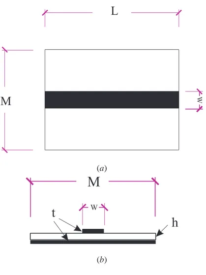
Let us consider the measurement sample composed by a section of short-ended microstrip trans-mission line (Fig. 1) and simply obtained by the photolitographic printing of a microstrip line on the planar substrate of MUT. Such a structure is characterized by a length L and a width M, w being the width of the microstrip transmission line. Moreover, t is the height of the
con-ductive strip and h is the height of the planar substrate of the MUT. Besides the geometrical
parameters, the electromagnetic behavior of the sample is determined by the conductivityσ of
the conductive parts and by the dielectric properties of the substrate [i.e., εr(f ) and tanδ (f )
of the MUT]. The two-port circuit is terminated on a short circuit and it is connected to a SMA coaxial connector on the other side, respectively. The input impedanceZinput is a function of
both the known geometrical parameters and the unknown dielectric properties of the sample under test
Zinput(f ) = Zinput{α, Λ (f )} (1)
where α = {L, M, w, h, t, σ} is the set of known quantities and Λ = {εr(f ) , tanδ (f )} is
the unknown array of the dielectric properties of the MUT to be characterized. The problem of the permittivity characterization is recast as on optimization one. Accordingly, let us define the cost functionΠ {Λ} aimed at quantifying the matching between simulated Zsim
inputand measured
Zmeas
input input impedance values at the sampling frequenciesfi,i = 1, ..., I
Π {Λ} = PI i=1 Z meas
input(fi) − Zinputsim (fi)
2 PI i=1 Z meas input(fi) 2 . (2)
In order to minimize (2), an iterative PSO-based procedure is used because of the complexity of the function at hand. The PSO is a robust stochastic search procedure, inspired by the social behavior of insects swarms, proposed by Kennedy and Eberhart in 1995 [17]. Thanks to its
features in exploring complex search spaces,PSO has been employed with success in different fields of electomagnetics ranging from from inverse scattering [18][19] and antenna design [20] up to transmission line matching [21]. As regards the problem at hand, the solution is yielded by integrating the PSO-based procedure with a method-of-moments (MoM) [22] electromagnetic
simulator devoted to the computation of the input impedanceZsim
inputin correspondence with a
PSO-estimated trial dielectric distribution. The full-wave electromagnetic simultor, developed at ELEDIALab, is able to compute the frequency behavior of the input impedance of the lenght
of microstrip transmission line taking into account its geometrical parameters, the
frequency-varying dielectric properties of the substrate, the short-circuit boundary condition at the end of
the transmission line and assuming as input section the line section at the opposite end. More specifically, the procedure considers a set of trial solutions Λ(k)p , p = 1, ..., P ; k = 0, ..., K (p
being the trial solution index andk the iteration index). Starting from a randomly-generated (in
the worst case when no a-priori information are available) initial setΛ(o)p , a succession of trial
solutions is generated according to the PSO strategy [17]. At each iterationk, the optimality of
the dielectric reconstruction is evaluated by computing with the MoM simulator the value of the cost functionΠ(k)opt in correspondence with the best trial solutionΛ
(k)
opt reached up till now (i.e.,
Λ(k)opt = arg
n
minp,k
h
ΠnΛ(k)p oio). The iterations stop when a maximum number is reached
(k = K) or when Π(k)opt ≤ η (η being an user-defined convergence threshold).
3
Numerical Simulation and Experimental Validation
In order to give an indication of the effectiveness of the proposed technique, two representative examples will be described in the remaining of this section.
The first test case is concerned with a sample of planar FR4 (αF R4 = {L = 80 mm, W =
120 mm, w = 10 mm, h = 1.6 mm, t = 35 µm, σ = 5.8 × 10⁻⁷S/m}). Moreover, the other
example considers a planar Arlon substrate (αArlon={L = 80 mm, W = 60 mm, w = 10 mm,
h = 0.8 mm, t = 35 µm, σ = 5.8 × 10⁻⁷S/m}). In order to reduce radiation phenomena
from microstrip line and in order to have non negligible attenuation phenomena the samples
for measurements and simulations are designed by using low characteristic impedance lines
(wider widths of the microstrip) and line lenght longer than a quarter of wavelenght. Figure 2 shows the photos of the two samples of MUT with the short circuits and equipped with the SMA connectors for the input impedance measurements. The short circuit have been made by using a copper sheet having width equal to that of the microstrip transmission line (according
the ground plane. In order to measure the input impedance just at the same input section of
the microstrip transmission line considered during simulations, before measurements the vector
network analyzer (Anritsu S332D) has been calibrated with an open circuit, a short circuit and
a matched load appositely built using three SMA connectors of the same type of that connected
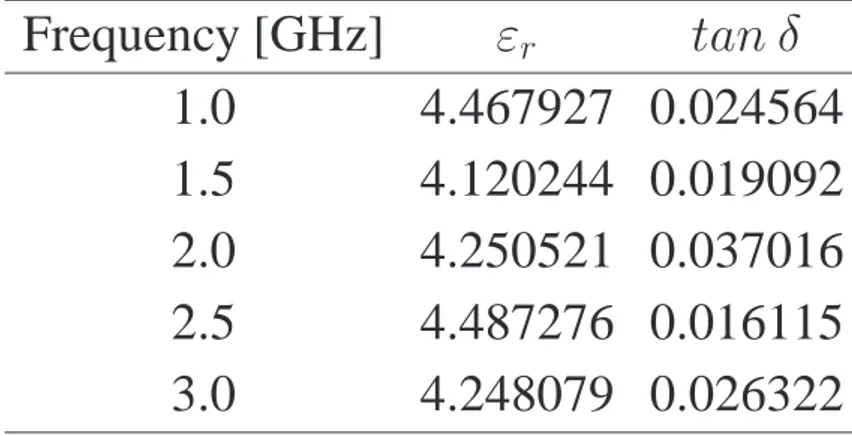
to the samples during impedance measurements. The input data for the reconstruction process have been measured at the frequencies f1 = 1.0 GHz, f2 = 1.5 GHz, f3 = 2.0 GHz, f4 =
2.5 GHz, and f5 = 3 GHz with a vector network analyzer by assuming the transverse plane
between the samples and the SMA connectors as reference/calibration section. As far as the PSO is concerned, the following setup has been used: a population of P = 5 trial solutions, a
threshold equal toη = 10−3, and a maximum amount ofK = 200 iterations.
Figure 3 shows the behavior of the cost function versus the iteration numberk for both the
MUT samples, while the values of the reconstructed permittivity at the frequencies of interest are given in Tabs. I-II, respectively. For completeness, the plots of the impedance values (sim-ulated and measured) are also reported Figs. 4-5 for a comparative assessment. In order to validate the obtained results, the permittivity values obtained with the described methodology
have been used to calculate the input impedance of the samples of transmission line under test
with an electromagnetic software different from that integrated in the proposed reconstruction
technique. To this end a finite-difference time-domain (FDTD) electromagnetic simulator has
been employed and the results have been compared with measurements. As expected (also from the value of the cost function at the convergence),there is a good agreement between simulated and measured data in correspondence with both materials and whatever the frequency value.
there is a good agreement between the measurements and the data calculated with the
recon-structed permittivity values at the same frequency values considered during the recostruction
process.
4
Conclusions
In this paper, a method for estimating the dielectric permittivity of planar substrates has been presented. It is based on the use of a PSO-based optimization strategy and it only requires the photolitographic building of one-port MUT samples as well as simple input impedance
mea-surements. For the experimental validation, two different planar substrates of different materials have been considered and the reconstruction results confirmed the reliability and effectiveness of the proposed approach.
References
[1] R. Azaro, M. Donelli, E. Zeni, and A. Massa, "Optimized synthesis of a miniaturized SARSAT band pre-fractal antenna," Microwave Optical Technol. Lett., vol. 48, no. 11, pp. 1031-1036, 2006.
[2] R. Azaro, E. Zeni, P. Rocca, and A. Massa, "Innovative design of a planar fractal-shaped GPS/GSM/Wi-Fi antenna," Microwave Optical Technol. Lett., vol. 50, no. 3, pp. 825-829, 2008.
[3] L. Lizzi, F. Viani, R. Azaro, and A. Massa, "Design of a miniaturized planar antenna for FCC-UWB communication systems," Microwave Optical Technol. Lett., vol. 50, no. 7, pp. 1975-1978, 2008.
[4] M. S. Razalli, A. Ismail, M. A. Mahdi, and M. N. bin Hamidon, “Novel compact mi-crostrip ultra-wideband filter utilizing short-circuited stubs with less vias,” Progress In
Electromagnetics Research, vol. PIER 88, pp. 91-104, 2008.
[5] M. L. Tounsi, R. Touhami, A. Khodja, and M. C. E. Yagoub, “Analysis of the mixed coupling in bilateral microwave circuits including anisotropy for Mics and Mmics appli-cations,” Progress In Electromagnetics Research, vol. PIER 62, pp. 281-315, 2006.
[6] S. Caorsi, M. Donelli, A. Massa, and M. Raffetto, "A parallel implementation of an evolutionary-based automatic tool for microwave circuit synthesis: preliminary results,"
Microwave Optical Technol. Lett., vol. 35, no. 3, pp. 169-172, 2002.
[7] N. Hamdi, A. Aguili, A. Bouallegue, and H. Baudrand, “A new technique for the analysis of discontinuities in microwave planar circuits,” Progress In Electromagnetics Research, vol. PIER 21, pp. 137-151, 1999.
[8] N. K. Das, S. M. Voda, and D. M. Pozar, “Two Methods for the Measurement of Substrate Dielectric Constant,” IEEE Trans. Microw. Theory Tech., vol. 35, no. 7, pp. 636-642, Jul
1987
[9] M.-Q. Lee and S. Nam, “An accurate broadband measurement of substrate dielectric con-stant,” IEEE Microwave and Guided Wave Letters, vol. 6, no. 4, pp. 168-170, Apr 1996
[10] R. Keam and A. D. Green, "Measurement of complex dielectric permittivity at microwave frequencies using a cylindrical cavity," Electron. Lett., vol. 31, no. 3, pp. 212-214, Feb. 1995.
[11] M. Olyphant and J. H. Ball, “Strip-line method for dielectric measurements at microwave frequencies,” IEEE Trans. Electr. Insul., vol. EI-5, no. 1, pp. 26-32, Mar. 1970.
[12] A. G. Gorriti and E. C. Slob, “A new tool for accurate S-parameters measurements and permittivity reconstruction,” IEEE Trans. Geosci. Remote Sens., vol. 43, no. 8, pp. 1727-1735, Aug. 2005.
[13] D. Misra, M. Chabbra, B. R. Epstein, M. Mirotznik, and K. R. Foster, “Noninvasive elec-trical characterization of materials at microwave frequencies using an open-ended coaxial line: test of an improved calibration technique,” IEEE Trans. Microw. Theory Tech., vol. 38, no. 1, pp. 8-14, Jan. 1990.
[14] M. D. Migliore, “Partial self-calibration method for permittivity measurement using trun-cated coaxial cable,” Electron. Lett., vol. 36, no. 15, pp. 1275-1277, Jul. 2000.
[15] T. W. Athey, M. A. Stuchly, and S. S. Stuchly, “Measurement of radio frequency permit-tivity of biological tissues with an open-ended coaxial line: Part 1,” IEEE Trans. Microw.
Theory Tech., vol. 30, no. 1, pp. 82-86, Jan. 1982.
[16] A. Ocera, M. Dionigi, E. Fratticcioli, and R. Sorrentino, “A novel technique for com-plex permittivity measurement based on a planar four-port device,” IEEE Trans. Microw.
[17] J. Robinson and Y. Rahmat-Samii, "Particle Swarm Optimization in Electromagnetics,"
IEEE Trans. Antennas Propag., vol. 52, no. 2, pp. 397-407, Feb. 2004.
[18] S. Caorsi, M. Donelli, A. Lommi, and A. Massa, ”Location and imaging of two-dimensional scatterers by using a particle swarm algorithm,” JEMWA, vol. 18, no. 4, pp. 481-494, 2004.
[19] M. Donelli, G. Franceschini, A. Martini, and A. Massa, ”An integrated multi- scaling strategy based on a particle swarm algorithm for inverse scattering problems,” IEEE Trans.
Geoscience Remote Sens., vol. 44, no. 2, pp. 298-312, Feb. 2006.
[20] M. Benedetti, G. Oliveri, P. Rocca, and A. Massa, “A fully-adaptive smart antenna prototype: ideal model and experimental validation in complex interference scenarios,”
Progress in Electromagnetic Research, vol. PIER 96, pp. 173-191, 2009.
[21] R. Azaro, F. De Natale, M. Donelli, and A. Massa, “PSO-based optimization of matching loads for lossy transmission lines,” Microw. Opt. Tech. Lett., vol. 48, no. 8, pp. 1485-1487, Aug. 2006.
[22] R. F. Harrington, Field Computation by Moment Methods. Malabar, FL: Robert E. Krieger, 1987.
FIGURE CAPTIONS
• Figure 1.Geometry of the MUT samples: (a) top view; (b) side view.
• Figure 2.MUT samples: (a) FR4 and (b) Arlon substrates.
• Figure 3. Iterative cost function minimization. Behaviour of the cost functions vs. the iteration number.
• Figure 4. FR4. Comparison between simulated and measuredimpedancevalues of (a)
Re {Z} and (b) Im {Z}.
• Figure 5. Arlon. Comparison between simulated and measuredimpedancevalues of (a)
Re {Z} and (b) Im {Z}.
TABLE CAPTIONS
• Table I.FR4. Reconstructedrelativepermittivity values(real part and loss tangent).
M
L
W (a) WM
t
h
(b)(a)
(b)
10-2 10-1 100 101 0 50 100 150 200 Iteration number k Πtot FR4 Πtot Arlon
20 15 10 5 0 3.5 3.0 2.5 2.0 1.5 1.0 0.5 ImpedanceRe(Z)[Ohm] Frequency [GHz] Simulated Measured (a) -300 -200 -100 0 100 200 300 3.5 3.0 2.5 2.0 1.5 1.0 0.5 Imped ance Im(Z)[Ohm] Frequency [GHz] Simulated Measured (b)
0 5 10 15 20 0.5 1.0 1.5 2.0 2.5 3.0 3.5
Impedance Re(Z) [Ohm]
Frequency [GHz] Simulated Measured (a) -300 -200 -100 0 100 200 300 0.5 1.0 1.5 2.0 2.5 3.0 3.5
Impedance Im(Z) [Ohm]
Frequency [GHz]
Simulated Measured
(b)